Effects of Acetone Vapor on the Exciton Band Photoluminescence Emission from Single- and Few-Layer WS2 on Template-Stripped Gold


1
Department of Chemistry, Natural Sciences Complex, University at Buffalo, The State University of New York, Buffalo, NY 14260-3000, USA
2
Department of Physics, Fronczak Hall, University at Buffalo, The State University of New York, Buffalo, NY 14260-3000, USA
*
Author to whom correspondence should be addressed.
Sensors 2019, 19(8), 1913; https://doi.org/10.3390/s19081913
Submission received: 13 March 2019
/
Revised: 17 April 2019
/
Accepted: 18 April 2019
/
Published: 23 April 2019
(This article belongs to the Special Issue Two-Dimensional Materials Based Sensors)
Abstract
:Two-dimensional (2D) materials are being used widely for chemical sensing applications due to their large surface-to-volume ratio and photoluminescence (PL) emission and emission exciton band tunability. To better understand how the analyte affects the PL response for a model 2D platform, we used atomic force microscopy (AFM) and co-localized photoluminescence (PL) and Raman mapping to characterize tungsten disulfide (WS2) flakes on template-stripped gold (TSG) under acetone challenge. We determined the PL-based response from single- and few-layer WS2 arises from three excitons (neutral, A0; biexciton, AA; and the trion, A−). The A0 exciton PL emission is the most strongly quenched by acetone whereas the A− PL emission exhibits an enhancement. We find the PL behavior is also WS2 layer number dependent.
1. Introduction
Transition metal dichalcogenides (TMDs), such as MX2, where M = Mo or W (but can be most transition metals from groups IV, V, VI, and VIII), and X = Se, S, or Te, consist of one metal atomic layer hexagonally packed between two chalcogenide atomic layers [1,2,3,4,5,6]. The metal possesses six-fold in-plane coordination and the chalcogenide layers can be trigonal or octahedral [1,2]. In the trigonal prismatic (2H) form, the TMD will be semiconducting; and in the octahedral form (1T), the TMD is metallic [3,6]. In either phase, the bond between the metal and chalcogen atom is covalent, and the layers are held together by weak van der Waals forces [4].
Transition metal dichalcogenides have been studied for many years because the bulk materials exhibit an indirect bandgap whereas their single-layer counterparts possess a direct bandgap [1,2,3,4,5]. Early thin layer TMD research focused on creating new, two-dimensional (2D) field-effect transistors (FETs), nanoelectronics, photo detectors, and sensors [7,8,9,10,11,12]. For example, conductance-/resistance-based measurements have been performed on single- and few-layer MoS2 to detect NO2, NH3, humidity, trimethylamine, acetone, and dichloromethane [9,10]. Resistance-based measurements using WS2 thin films at 150 °C, exhibit sensitivity to H2, NH3, and NO2 [12]. Similarly, Huo et al. [11] reported O2, air, EtOH, and NH3 sensing by using single- and few-layer WS2 as photo detectors. Theoretical first-principles studies [13,14] have suggested that adsorbed NO, O2, H2O, and CO molecules on single- and few-layer WS2 can change the WS2 electronic and optical properties, making WS2 an attractive candidate for room temperature gas sensing platforms. In addition, Cho et al. [15] used photoluminescence (PL)-based measurements on single- and few-layer MoS2 to detect NO2 and NH3. To the best of our knowledge, there has yet to be any report exploiting the PL emission from single- and few-layer WS2 for chemical sensing. We have chosen WS2 as our model TMD because the PL emission from single-layer WS2 is 20 to 40 times more intense in comparison to single-layer MoS2 [16], and, where the PL gradually decreases with increasing film thickness in WS2, there is a drastic decrease from single- to bi-layer MoS2 [17].
WS2 has three main Raman active phonon modes (2LA(M), ~350 cm−1; E12g, ~355 cm−1; and A1g, ~418 cm−1) [2,4]. The difference in energy between the E12g and A1g bands (Δ) and the 2LA/A1g intensity ratio depends on the number of WS2 layers [2]. Single- and few-layer WS2 also exhibits a strong PL emission and the emission spectrum arises from three excitons [4,18], including the neutral exciton (A0, an electron and hole bound together), biexciton (AA, two neutral excitons bound weakly), and trion (A−, two electrons and one hole). Previous single point PL emission experiments [15] on single-layer MoS2 specimens have shown that the A0 and A− exciton bands behave differently when different gaseous vapors pass over the 2D specimen. For example, NO2 (electron acceptor)/NH3 (electron donor) vapors cause the A− band amplitude to increase/decrease whereas the A0 band amplitude to decrease/increase [15].
Although most research has studied WS2 on SiO2/Si substrates, we chose gold substrates because of their applications in tip-enhanced Raman scattering (TERS) spectroscopy to enhance the Raman and PL signal and allow improved spatial resolution and scanning Kelvin probe microscopy (SKPM), to study the specimen’s electronic properties.
In this paper, we determine the acetone-induced changes in the A0, AA, and A− exciton band amplitude, peak energy, and energy distribution across individual WS2 flakes that consist of single- and few-layer regions by using co-localized, confocal Raman, and PL emission mapping experiments.
2. Materials and Methods
2.1. WS2 Materials and Supplies
The following were used: Acetone (Fisher Scientific, Hampton, NH, USA); Ar gas (Jackson Welding&Gas Products, Buffalo, NY, USA); N2 gas (Airgas, Randor, PA, USA); polymethyl methacrylate (PMMA) (MW 120K, Sigma Aldrich, St. Louis, MO, USA); sulfur (≥99.95% purity, Alfa Aesar, Haverhill, MA, USA); tetrahydrofuran (THF, HPLC grade (Pharmco-Aaper, Brookfield, USA)); WO3 (99.98% purity, Acros Organics, VWR, Randor, PA, USA); Au evaporation pellets (Kurt J. Lesker Co., Jefferson Hills, PA, USA); Epo-Tek 377 epoxy (Epoxy Technology, Billerica, MA, USA); p-type, boron-doped silicon wafers (<100>) (650 to 690 µm thickness and 1 to 10 Ω·cm resistivity, Alsil Supply Division Ymart, Palm Beach Gardens, FL, USA); and sapphire substrates (Hefei Keijing Materials Technology, Hefei, China).
2.2. 2D WS2 Fabrication
Ultrathin WO3 films were deposited by electron beam evaporation onto sapphire substrates by using an ATC Series UHV dual chamber deposition system. These films, along with S were placed in consecutive zones inside a quartz furnace tube. A simplified diagram depicting the fabrication scheme [19] can be found in the Supplementary Materials in Figure S3. Zone 1 contained ~4 to 8 mg of S and was placed 30 cm upstream from zone 2, which held the WO3 film. Both zones had independently controlled temperatures, and the temperature ramping profiles were used to control the S vapor pressure at the WS2 growth temperature. The carrier gas was N2 with a flow rate of 40 standard cubic centimeters per minute (sccm) at ambient pressure. The zone 1 source temperature (containing S) was increased to 190 °C at a rate of 6 °C/min, and heating of this zone was stopped after 5 min. The temperature in zone 2 was increased at the same time as zone 1 to 745 °C at a rate of 25 °C/min. The temperature was then kept at 745 °C for 5 min to allow WS2 growth. After the 5 min growth time, the heaters and N2 flow were turned off to obtain single layer WS2 with some few layer overgrowth. A proposed WS2 from the WO3 mechanism has been described elsewhere [19,20].
2.3. Template Stripped Gold (TSG) Fabrication
Template stripped gold was created in several steps [21]. Initially, 125 nm of Au was deposited onto an Si wafer by e-beam evaporation (AXXIS electron-beam evaporator with glancing angle deposition (Kurt J. Lesker Co.). This Au-coated wafer was cut into roughly 1 cm × 1 cm squares by using a diamond tip cutter. A second Si wafer, without Au coating, was cut into roughly 1.5 cm × 1.5 cm squares by using a diamond tipped cutter. A drop of epoxy was placed on the Au-coated Si wafer and the uncoated Si wafer was placed on top of this, effectively sandwiching the Au. The sample was then cured in an oven at 150 °C for 1 h. After cooling, the epoxy “sandwich” was placed in a beaker of THF for 1 h to facilitate the separation between the Au and the Si wafer it was deposited on. The resulting substrate was an ultra-flat Au surface with an RMS (root mean square) roughness of ~0.7 nm.
2.4. WS2 Exfoliation onto TSG
WS2 samples were exfoliated onto TSG films by using the “water droplet method” [22]. Briefly, PMMA (1.2 M) was dissolved in chlorobenzene and spin coated onto the WS2 flakes prepared atop a sapphire substrate. After 5 min at 80 °C, a water droplet was placed on top of the PMMA layer and the PMMA edge was poked with a sharp tweezer to allow water to penetrate underneath the WS2 layer; this resulted in WS2-sapphire separation. The resulting PMMA-WS2 film was then transferred onto the TSG and heated for 10 min at 80 °C to remove water. The PMMA was then dissolved away by using acetone.
2.5. Raman, AFM, and PL Instrumentation
All Raman and PL measurements were performed by using a LabRam HR (Horiba, Edison, NJ, USA) with a 100× objective (LM Plan FL N, NA = 0.80, Olympus, Center Valley, PA, USA). The excitation source was a 532.06 nm laser (Laser Quantum, Fremont, CA, USA). Detection was performed by using a one-electrode thermoelectrically cooled CCD detector (Andor Technology Inc., Belfast, Northern Ireland). The entire system was controlled by LabSpec 6 software (Horiba).
Atomic force microscopy (AFM) measurements were recorded by using an AIST-NT model SmartSPM 1000 in intermittent contact mode with an Al-coated Si probe (k = 2 N/m, 240 µm length) (AC240TM-R3, Oxford Instruments Asylum Research, Santa Barbara, CA, USA) operating at a 70 kHz resonant frequency and controlled by Omega software 3.5.81 (AIST-NT).
2.6. AFM and Raman Studies
Atomic force microscopy height and phase images were recorded from 10 µm × 10 µm areas at a 512 × 512-pixel resolution (ca., 19.5 nm/step). Co-localized Raman and PL emission maps were acquired from 10 µm × 10 µm areas at a 64 × 64-pixel resolution (ca., 156 nm/step). All Raman and PL experiments were performed by using 600 and 300 grooves/mm gratings, respectively, yielding 1.6 cm−1 and 3.1 nm spectral resolutions, respectively. The incident laser power density for all Raman and PL experiments was 510 W/cm2 and 130 W/cm2, respectively. All image and maps were recorded at 1.0 Hz/pixel.
2.7. Gaseous Analyte Vapor Studies
The WS2 specimens were placed within a custom-built Teflon flow cell with a glass optical port. The flow cell was maintained at room temperature (294–296 K) while the WS2 specimen was subjected to air or acetone vapor environments. The air/acetone cycle was performed at least three times on the same specimen to determine reproducibility (no detectable hysteresis). At least three specimens were assessed. Typical results are shown.
3. Results and Discussion
3.1. Layer Thickness Determination
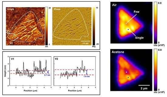
Figure 1a presents typical AFM height (left) and phase (right) images from a WS2 flake on TSG. The WS2 appears to be wrinkled and ridges in the height image correspond to areas with low phase values (e.g., −20°) whereas regions that appear less wrinkled have more uniform, higher phase values (e.g., +10°). Phase imaging in AFM is a measure of the energy dissipation between the AFM probe tip and the sample. This depends on many factors, including specimen-to-substrate adhesion [23] (pp. 69–71). In our case, a lower phase value indicates lower adhesion between regions within the WS2 flake and the Au substrate while higher phase values indicate greater adhesion between regions within the WS2 flake area and the Au substrate. The results shown in Figure 1a are consistent with WS2 flakes that are wrinkled on the TSG surface where the WS2 ridges are in poor contact with the Au substrate.
In Figure 1b, we present AFM height profiles along the two vectors shown in Figure 1a (left). The V1 vector traverses a pathway that is largely single-layer WS2 and the V2 vector follows a path that appears to be largely composed of two-layer WS2. Unfortunately, the WS2 wrinkles make it very challenging to assess our WS2 flake thickness by using AFM alone.
Figure 2 presents typical diffraction limited, single-point Raman spectra recorded at WS2 flake edges devoid of wrinkles that were determined by AFM height measurements to be either single- (Figure 2a) or few-layer (Figure 2b). All detectable Raman bands are labeled [2], including the key 2LA, E12g, and A1g bands. Using the known AFM-derived height at specific locations across a WS2 flake, the boxed insets in Figure 2a,b show that the I2LA/IA1g and Δ (difference in the 2LA-A1g band maxima) are layer number dependent and can be readily used to distinguish single- and few-layer WS2 even on a heavily wrinkled specimen.
Figure 3 presents typical Raman-based mapping results from an isolated WS2 flake on TSG. Figure 3a,b illustrate the I2LA/IA1g- and Δ-based maps, respectively (the original 2LA and A1g intensity and position maps can be found in the Supplementary Materials in Figures S1 and S2). Figure 3c presents a layer count map created by multiplying Figure 3a,b. An inspection of these data shows that this particular WS2 flake has a center region that consists of few-layer (mostly two-layer) WS2 and the flake remainder is composed, largely, of single-layer WS2.
3.2. Acetone Effect on WS2 Flake Total PL and Exciton Band Emission
Figure 4 presents typical total PL emission intensity (1.8–2.1 eV) maps for the WS2 flake shown in Figure 3 under air (Figure 4a) or acetone vapor atmospheres (Figure 4b). Two specific locations on this WS2 flake are labeled in Figure 4a, denoting regions that are composed of single- (black circle) and few-layer (white circle) WS2. These locations were selected based on the material classification scheme shown in Figure 3. Figure 4c presents the PL intensity ratio (PLAir/PLAcetone) map from the data in Figure 4a,b. An inspection of these data shows that the PL emission intensity: (i) Is heterogeneous across the WS2 flake when it is under air or acetone vapor, (ii) is generally quenched by acetone vapor, and (iii) quenching is heterogeneous across the WS2 flake. The largest extent of PL quenching is observed at the flake’s middle and upper and lower edges, where the flake is mostly composed of few-layer WS2 (cf., Figure 3). Thus, there is a strong spatial dependence in the acetone-induced PL emission quenching from a WS2 flake.
Figure 5 present typical diffraction limited, single-point PL emission spectra from the WS2 specimen shown in Figure 3 measured at locations within the flake (cf., Figure 3c) that are composed of single- (Figure 5a) or few-layer (Figure 5b) WS2. Within each panel series are spectra recorded in air (1) and under acetone vapor (2) plus the corresponding PL emission energy-dependent PLAir/PLAcetone response spectra (3). The dashed line in spectra 3 (located at 1.0) denotes where there is no detectable PL emission quenching. Energy regions with PLAir/PLAcetone values < 1 exhibit acetone-induced PL enhancement whereas energy regions with PLAir/PLAcetone values > 1 exhibit acetone-induced PL quenching. The PL emission spectra labeled 1 and 2 were individually curve fitted to models having two or three exciton emission bands (Gaussian). The best fit (r2 > 0.99) was observed for a three band model and is consistent with emission from the A0, AA, and A− excitons as reported by other researchers [4,18,24]. The general assignment of each WS2 exciton band in the current research is based on previous reports in the literature [4,16,18,24]. We have also noticed that the AA exciton band exhibits a laser power-dependent position shift and a non-linear increase in amplitude with increasing laser power (results not shown). This behavior is consistent with an AA exciton being present [16]. Together, these data show that there are dramatic differences in the A0, AA, and A− exciton emission susceptibility and response to acetone vapors and also a strong WS2 layer number dependency. This has significant ramifications in the construction of PL-based sensors using such a platform and illustrates several potential opportunities for the creation of a tailored sensor response. For example, in quenchometric sensors [25,26], the quencher (Q) causes the PL emission intensity (PL) to decrease in a Q-dependent manner [25,26]. A response curve is created by plotting PL0/PLanalyte vs. [Q], where PL0 and PLanalyte represent the PL emission intensities in the absence and presence of Q, respectively. An ideal quenchometric sensor exhibits a response curve with high sensitivity (i.e., d((PL0/PLanalyte)/d[Q]) [25,26].
Figure 6, Figure 7 and Figure 8 present typical A0, AA, and A− PL emission exciton band amplitude, band maxima (eV), and band full width at half maximum (FWHM) (eV) maps, respectively, for the WS2 flake shown in Figure 3 and Figure 4. These air- and acetone-dependent exciton species maps were created by curve fitting the individual PL emission spectra in air and under acetone vapor at each pixel within the region of interest (4096 separate spectra) as described in Figure 5.
Figure 9 summarizes the impact of acetone vapor on the A0, AA, and A− exciton emission bands from an individual WS2 flake on TSG. Several aspects of these results merit further discussion. In a general sense, the response depends on the emission exciton type and WS2 layer number. The A0 exciton from single-layer WS2 exhibits the highest acetone-induced quenching sensitivity (PLAir/PLAcetone up to 20). The A0 exciton from few-layer WS2 exhibits an acetone-induced quenching sensitivity that is generally 1/4 the corresponding single-layer value. The AA exciton from single-layer WS2 is only 1/3 as sensitive (PLAir/PLAcetone up to 7) to acetone-induced quenching in comparison to the single-layer A0 exciton. The AA exciton from few-layer WS2 is not particularly sensitive to acetone-induced quenching (1.0 > PLAir/PLAcetone < 1.5). The A− exciton exhibits unique PL emission behaviors. The A− exciton from few-layer WS2 exhibits only modest acetone-induced quenching sensitivity (1.1 > PLAir/PLAcetone < 1.5). Interestingly, the A− exciton band from the lion’s share of single-layer WS2 is the only band within the flake to exhibit an acetone-induced PL emission enhancement (0.1 > PLAir/PLAcetone < 0.5). It is well known that acetone acts as an electron donor in the presence of MoS2 and WS2 [9,15,27,28]. A previous study on MoS2 [15] shows that the positive trion (one electron, two holes, A+) band amplitude decreases in the presence of an electron donor, and the authors reasoned that when additional electrons are introduced from an electron donor, the PL spectrum is suppressed because of dissociation of the positive trions from the neutral excitons (A0). We determine the enhancement seen in our results is from the negative trion (two electrons, one hole, A−) accepting additional electrons from the electron donor, which results in an increase in the PL spectrum for the A−.
Acetone also induces detectable shifts in the exciton emission band energies. The energy shifts in the A0 exciton emission band across the WS2 flake are the least distinct, but there are up to +30 meV shifts from regions that also exhibit the highest acetone susceptibilities (single-layer WS2). The energy shifts within the few-layer region are very small (just +5 meV) for the A0 exciton emission band. The energy shifts in the AA exciton emission band across the WS2 flake produces a very distinct pattern. In the single-layer region, the acetone-induced shift is up to −10 meV. In the few-layer region, the corresponding shift is up to −50 meV. This could arise from the topmost WS2 layer within the few-layer region. The energy shifts in the A− exciton band emission across the WS2 flake produces another distinct pattern. In the single-layer region, the acetone-induced shift is small (0 to +10 meV). In the few-layer region, the corresponding shift is up to +20 meV.
The exciton band FWHM also changes under acetone vapor. The FWHM shifts in the A0 exciton emission band across the WS2 flake show very modest effects (−10 to +10 meV), but the more positive shifts appear in areas with large energy differences and the highest sensitivity to acetone quenching. The FWHM shifts in the AA exciton emission band across the WS2 flake exhibit an interesting pattern. In single-layer WS2 regions with high AA exciton emission band sensitivity to acetone, the band FWHM shift is up to +60 meV. In the few-layer WS2 region, the band FWHM shifts are slightly larger (up to +80 meV). This could arise from the topmost WS2 layer within the few-layer region. The exciton emission band FWHM shifts in the A− exciton band across the WS2 flake exhibit a striking pattern. In the single-layer region, the band FWHM shifts are generally −50 to −80 meV, but there are regions with −20 meV shifts at the flake edges that also correspond to a high PL quenching sensitivity. In the immediate area surrounding the few-layer region, the FWHM shifts are the largest (up to −100 meV). This area corresponds to the region where acetone-induced PL enhancement is observed.
Figure 10 is a model to summarize the single- and few-layer WS2 exciton PL emission behavior in the presence of acetone. Acetone causes an overall decrease in the A0 and AA exciton band PL emission for single- and few-layer WS2. A decrease in PL emission was also produced in the A− exciton band PL emission in few-layer WS2, but there is an overall increase in the A− exciton band PL emission from single-layer WS2.
4. Conclusions
Atomic force microscopy, Raman, and PL maps were used to determine the WS2 layer thickness and map the A0, AA, and A− PL emission exciton band contribution within the flake for chemical sensing assessment. Analyte vapor studies show that the PL response from the WS2 flake is exciton-type and layer number dependent. It has been shown that the exciton amplitude, energy, and FWHM are all affected by acetone vapor. The A0 exciton PL emission is most strongly quenched by acetone whereas the A− exciton PL emission shows a unique PL enhancement under acetone vapors. The results identify interesting strategies to generate unique, analyte-dependent responses from single- and few layer WS2 platforms. We are currently investigating single- and few-layer WS2 PL exciton band behavior on sapphire and SiO2/Si substrates.
Supplementary Materials
The following are available online at https://www.mdpi.com/1424-8220/19/8/1913/s1, Figure S1: Initial Raman maps and layer count ratio. Figure S2: Initial Raman maps and layer count difference. Figure S3: Simplified schematic depicting WS2 fabrication.
Author Contributions
S.M. contributed to the acquisition, analysis, and interpretation of data, and drafting the original manuscript. C.Z. contributed to the fabrication of the material. H.Z. contributed to the review and editing of the manuscript. F.V.B. contributed to the conceptualization, data interpretation, and manuscript preparation and editing.
Funding
This research was funded by the National Science Foundation, grant number CHE-1411435. Any opinions, findings, and conclusions or recommendations expressed in this material are those of the authors and do not necessarily reflect the views of the National Science Foundation.
Acknowledgments
The authors would like to thank Gary Nottingham from the UB College of Arts and Sciences Machine Shop for designing and fabricating the Teflon flow cell used in this research.
Conflicts of Interest
The authors declare no conflict of interest.
References
- Rout, C.S.; Joshi, P.D.; Kashid, R.V.; Joag, D.S.; More, M.A.; Simbeck, A.J.; Washington, M.; Nayak, S.K.; Late, D.J. Superior Field Emission Properties of Layered WS2-RGO Nanocomposites. Sci. Rep. 2013, 3, 1–8. [Google Scholar] [CrossRef] [PubMed]
- Berkdemir, A.; Gutiérrez, H.R.; Botello-Méndez, A.R.; Perea-López, N.; Elías, A.L.; Chia, C.-I.; Wang, B.; Crespi, V.H.; López-Urías, F.; Charlier, J.-C.; et al. Identification of Individual and Few Layers of WS2 Using Raman Spectroscopy. Sci. Rep. 2013, 3, 1–8. [Google Scholar] [CrossRef]
- Lv, R.; Robinson, J.A.; Schaak, R.E.; Sun, D.; Sun, Y.; Mallouk, T.E.; Terrones, M. Transition Metal Dichalcogenides and Beyond: Synthesis, Properties, and Applications of Single- and Few-Layer Nanosheets. Acc. Chem. Res. 2015, 48, 56–64. [Google Scholar] [CrossRef]
- Mitioglu, A.A.; Plochocka, P.; Jadczak, J.N.; Escoffier, W.; Rikken, G.L.J.A.; Kulyuk, L.; Maude, D.K. Optical Manipulation of the Exciton Charge State in Single Layer Tungsten Disulfide. Phys. Rev. B 2013, 88, 1–5. [Google Scholar] [CrossRef]
- Zhao, W.; Ghorannevis, Z.; Chu, L.; Toh, M.; Kloc, C.; Tan, P.-H.; Eda, G. Evolution of Electronic Structure in Atomically Thin Sheets of WS2 and WSe2. ACS Nano 2013, 7, 791–797. [Google Scholar] [CrossRef] [PubMed]
- Yoffe, A.D. Layer Compounds. Annu. Rev. Mater. Res. 1973, 3, 147–170. [Google Scholar] [CrossRef]
- Thripuranthaka, M.; Late, D.J. Temperature Dependent Phonon Shifts in Single-Layer WS2. ACS Appl. Mater. Interfaces 2014, 6, 1158–1163. [Google Scholar]
- Kotlyar, R.; Avci, U.E.; Cea, S.; Rios, R.; Linton, T.D.; Kuhn, K.J.; Young, I.A. Bandgap Engineering of Group IV Materials for Complementary n and p Tunneling Field Effect Transistors. Appl. Phys. Lett. 2013, 102, 1–4. [Google Scholar] [CrossRef]
- Late, D.J.; Huang, Y.-K.; Liu, B.; Acharya, J.; Shirodkar, S.N.; Luo, J.; Yan, A.; Charles, D.; Waghmare, U.V.; Dravid, V.P.; et al. Sensing Behavior of Atomically Thin-Layered MoS2 Transistors. ACS Nano 2013, 7, 4879–4891. [Google Scholar] [CrossRef]
- Perkins, F.K.; Friedman, A.L.; Cobas, E.; Campbell, P.M.; Jernigan, G.G.; Jonker, B.T. Chemical Vapor Sensing with Monolayer MoS2. Nano Lett. 2013, 13, 668–673. [Google Scholar] [CrossRef]
- Huo, N.; Yang, S.; Wei, Z.; Li, S.S.; Xia, J.B.; Li, J. Photoresponsive and Gas Sensing Field-Effect Transistors Based on Multilayer WS2 Nanoflakes. Sci. Rep. 2014, 4, 1–9. [Google Scholar] [CrossRef]
- Perrozzi, F.; Emamjomeh, S.M.; Paolucci, V.; Taglieri, G.; Ottaviano, L.; Cantalini, C. Thermal Stability of WS2 Flakes and Gas Sensing Properties of WS2/WO3 Composite to H2, NH3, and NO2. Sens. Actuators B Chem. 2017, 243, 812–822. [Google Scholar] [CrossRef]
- Bui, V.Q.; Pham, T.T.; Le, D.A.; Thi, C.M.; Le, H.M. A First-Principles Investigation of Various Gas (CO, H2O, NO, and O2) Absorptions on a WS2 Monolayer: Stability and Electronic Properties. J. Phys. Condens. Matter 2015, 27, 1–11. [Google Scholar] [CrossRef]
- Donarelli, M.; Ottaviano, L. 2D Materials for Gas Sensing Applications: A Review on Graphene Oxide, MoS2, WS2 and Phosphorene. Sensors 2018, 18, 3638. [Google Scholar] [CrossRef]
- Cho, B.; Hahm, M.G.; Choi, M.; Yoon, J.; Kim, A.R.; Lee, Y.J.; Park, S.G.; Kwon, J.D.; Kim, C.S.; Song, M.; et al. Charge-Transfer-Based Gas Sensing Using Atomic-Layer MoS2. Sci. Rep. 2015, 5, 1–6. [Google Scholar] [CrossRef]
- Gutierrez, H.R.; Perea-Lopez, N.; Elias, A.L.; Berkdemir, A.; Wang, B.; Lv, R.; Lopez-Urias, F.; Crespi, V.H.; Terrones, H.; Terrones, M. Extraordinary Room-Temperature Photoluminescence in Triangular WS2 Monolayers. Nano Lett. 2013, 13, 3447–3454. [Google Scholar] [CrossRef]
- Eda, G.; Yamaguchi, H.; Voiry, D.; Fujita, T.; Chen, M.; Chhowalla, M. Photoluminescence from Chemically Exfoliated MoS2. Nano Lett. 2011, 11, 5111–5116. [Google Scholar] [CrossRef] [PubMed]
- Kim, M.S.; Yun, S.J.; Lee, Y.; Seo, C.; Han, G.H.; Kim, K.K.; Lee, Y.H.; Kim, J. Biexciton Emission from Edges and Grain Boundaries of Triangular WS2 Monolayers. ACS Nano 2016, 10, 2399–2405. [Google Scholar] [CrossRef]
- Taheri, P.; Wang, J.; Xing, H.; Destino, J.F.; Arik, M.M.; Zhao, C.; Kang, K.; Blizzard, B.; Zhang, L.; Zhao, P.; et al. Growth Mechanism of Largescale MoS2 Monolayer by Sulfurization of MoO3 Film. Mater. Res. Express 2016, 3, 1–10. [Google Scholar] [CrossRef]
- Cong, C.; Shang, J.; Wu, X.; Cao, B.; Peimyoo, N.; Qiu, C.; Sun, L.; Yu, T. Synthesis and Optical Properties of Large-Area Single-Crystalline 2D Semiconductor WS2 Monolayer from Chemical Vapor Deposition. Adv. Opt. Mater. 2014, 2, 131–136. [Google Scholar] [CrossRef]
- Hegner, M.; Wagner, P.; Semenza, G. Ultralarge Atomically Flat Template-Stripped Au Surfaces for Scanning Probe Microscopy. Surf. Sci. 1993, 291, 39–46. [Google Scholar] [CrossRef]
- Gurarslan, A.; Yu, Y.; Su, L.; Yu, Y.; Suarez, F.; Yao, S.; Zhu, Y.; Ozturk, M.; Zhang, Y.; Cao, L. Surface-Energy-Assisted Perfect Transfer of Centimeter-Scale Monolayer and Few-Layer MoS2 Films onto Arbitrary Substrates. ACS Nano 2014, 8, 11522–11528. [Google Scholar] [CrossRef] [PubMed]
- Eaton, P.; West, P. AFM Modes. In Atomic Force Microscopy; Oxford University Press: Oxford, UK, 2010; pp. 69–71. [Google Scholar]
- Zhao, W.; Ribeiro, R.M.; Toh, M.; Carvalho, A.; Kloc, C.; Castro Neto, A.H.; Eda, G. Origin of Indirect Optical Transitions in Few-Layer MoS2, WS2, and WSe2. Nano Lett. 2013, 13, 5627–5634. [Google Scholar] [CrossRef] [PubMed]
- Lakowicz, J.R. Quenching of Fluorescence. In Principles of Fluorescence Spectroscopy; Kluwer Academic/Plenum Publishers: New York, NY, USA, 2013; pp. 278–281. [Google Scholar]
- Bukowski, R.M.; Ciriminna, R.; Pagliaro, M.; Bright, F.V. High-Performance Quenchometric Oxygen Sensors Based on Fluorinated Xerogels Doped with [Ru(dpp)3]2+. Anal. Chem. 2005, 77, 2670–2672. [Google Scholar] [CrossRef] [PubMed]
- Ko, K.Y.; Song, J.-G.; Kim, Y.; Choi, T.; Shin, S.; Lee, C.W.; Lee, K.; Koo, J.; Lee, H.; Kim, J.; et al. Improvement of Gas-Sensing Performance of Large-Area Tungsten Disulfide Nanosheets by Surface Functionalization. ACS Nano 2016, 10, 9287–9296. [Google Scholar] [CrossRef]
- Friedman, A.L.; Perkins, F.K.; Cobas, E.; Jernigan, G.G.; Campbell, P.M.; Hanbicki, A.T.; Jonker, B.T. Chemical Vapor Sensing of Two-Dimensional MoS2 Field Effect Transistor Devices. Solid State Electron. 2014, 101, 2–7. [Google Scholar] [CrossRef]
Figure 1.
Typical AFM results for a WS2 flake on TSG. (a) Typical AFM height (left) and phase (right) images. The dotted curve is used to outline the WS2 flake. Two vectors (V1 and V2) are shown in the height image. (b) Typical height profiles along the V1 (left) and V2 (right) vectors shown in panel a. The V1 and V2 vectors traverse largely single- and two-layer regions, respectively.

Figure 2.
Typical single point Raman spectra and band assignments for different areas on a WS2 flake on TSG. (a) Single-layer region. (b) Few-layer region.
Figure 2.
Typical single point Raman spectra and band assignments for different areas on a WS2 flake on TSG. (a) Single-layer region. (b) Few-layer region.

Figure 3.
Typical WS2 layer count maps for a single WS2 flake on TSG. (a) I2LA/IA1g intensity ratio map. (b) Δ (E2LA − EA1g) band energy difference map. (c) Combined a and b WS2 layer count map.
Figure 3.
Typical WS2 layer count maps for a single WS2 flake on TSG. (a) I2LA/IA1g intensity ratio map. (b) Δ (E2LA − EA1g) band energy difference map. (c) Combined a and b WS2 layer count map.

Figure 4.
Typical total PL emission intensity maps (1.8–2.1 eV) for a single WS2 flake on TSG. (a) Air atmosphere. (b) Acetone atmosphere. (c) PLAir/PLAcetone intensity response map. The black and white dots indicate single- and few-layer WS2 regions determined from Figure 3c.
Figure 4.
Typical total PL emission intensity maps (1.8–2.1 eV) for a single WS2 flake on TSG. (a) Air atmosphere. (b) Acetone atmosphere. (c) PLAir/PLAcetone intensity response map. The black and white dots indicate single- and few-layer WS2 regions determined from Figure 3c.

Figure 5.
Typical single point PL emission spectra and curve fits from specific locations on the WS2 flake shown in Figure 4. (a) Spectra from a single-layer WS2 region. (b) Spectra from a few-layer WS2 region. (1) Spectra recorded in air. (2) Spectra recorded under acetone vapor. (3) Energy-dependent PLAir/PLAcetone response spectra. The dashed line in spectra 3 located at 1.0 denotes no quenching. Spectral regions with PLAir/PLAcetone < 1 exhibit a PL enhancement under acetone vapor. Spectral regions with PLAir/PLAcetone > 1 exhibit a PL quench under acetone vapor.

Figure 6.
Typical PL emission A0, AA, and A− exciton band amplitude maps for a single WS2 flake on TSG under air and acetone vapors. Maps are generated by curve fitting PL emission spectra at each pixel across the entire flake. (a,b,c) Maps in air. (d,e,f) Maps under acetone vapor.
Figure 6.
Typical PL emission A0, AA, and A− exciton band amplitude maps for a single WS2 flake on TSG under air and acetone vapors. Maps are generated by curve fitting PL emission spectra at each pixel across the entire flake. (a,b,c) Maps in air. (d,e,f) Maps under acetone vapor.

Figure 7.
Typical PL emission A0, AA, and A− exciton band maxima (eV) maps for a single WS2 flake on TSG under air and acetone vapors. Maps are generated by curve fitting PL emission spectra at each pixel across the entire flake. (a,b,c) Maps in air. (d,e,f) Maps under acetone vapor.
Figure 7.
Typical PL emission A0, AA, and A− exciton band maxima (eV) maps for a single WS2 flake on TSG under air and acetone vapors. Maps are generated by curve fitting PL emission spectra at each pixel across the entire flake. (a,b,c) Maps in air. (d,e,f) Maps under acetone vapor.

Figure 8.
Typical PL emission A0, AA, and A− exciton band FWHM (eV) maps for a WS2 flake on TSG under air and acetone vapors. Maps are generated by curve fitting PL emission spectra at each pixel across the entire flake. (a,b,c) Maps in air. (d,e,f) Maps under acetone vapor.
Figure 8.
Typical PL emission A0, AA, and A− exciton band FWHM (eV) maps for a WS2 flake on TSG under air and acetone vapors. Maps are generated by curve fitting PL emission spectra at each pixel across the entire flake. (a,b,c) Maps in air. (d,e,f) Maps under acetone vapor.

Figure 9.
Typical acetone vapor-dependent PL emission A0, AA, and A− exciton band intensity ratio (PLAir/PLAcetone), band energy maxima difference (Emax,Air − Emax,Acetone), and band FWHM energy difference (FWHMAir − FWHMAcetone) maps for a single WS2 flake on TSG.
Figure 9.
Typical acetone vapor-dependent PL emission A0, AA, and A− exciton band intensity ratio (PLAir/PLAcetone), band energy maxima difference (Emax,Air − Emax,Acetone), and band FWHM energy difference (FWHMAir − FWHMAcetone) maps for a single WS2 flake on TSG.

Figure 10.
Model of the overall effect of acetone on exciton bands. A WS2 flake in an air environment denoting single- and few-layer areas. The red arrows indicate a quench in PL and the blue arrow indicates an enhancement. The arrow length represents the effect magnitude.
Figure 10.
Model of the overall effect of acetone on exciton bands. A WS2 flake in an air environment denoting single- and few-layer areas. The red arrows indicate a quench in PL and the blue arrow indicates an enhancement. The arrow length represents the effect magnitude.

© 2019 by the authors. Licensee MDPI, Basel, Switzerland. This article is an open access article distributed under the terms and conditions of the Creative Commons Attribution (CC BY) license (http://creativecommons.org/licenses/by/4.0/).
Share and Cite
MDPI and ACS Style
Matthews, S.; Zhao, C.; Zeng, H.; Bright, F.V. Effects of Acetone Vapor on the Exciton Band Photoluminescence Emission from Single- and Few-Layer WS2 on Template-Stripped Gold. Sensors 2019, 19, 1913. https://doi.org/10.3390/s19081913
AMA Style
Matthews S, Zhao C, Zeng H, Bright FV. Effects of Acetone Vapor on the Exciton Band Photoluminescence Emission from Single- and Few-Layer WS2 on Template-Stripped Gold. Sensors. 2019; 19(8):1913. https://doi.org/10.3390/s19081913
Chicago/Turabian StyleMatthews, Samantha, Chuan Zhao, Hao Zeng, and Frank V. Bright. 2019. "Effects of Acetone Vapor on the Exciton Band Photoluminescence Emission from Single- and Few-Layer WS2 on Template-Stripped Gold" Sensors 19, no. 8: 1913. https://doi.org/10.3390/s19081913
Note that from the first issue of 2016, this journal uses article numbers instead of page numbers. See further details here.