Introduction
Humidity is a constant environmental factor; therefore its accurate measurement and control are very important. Humidity sensors are generally required in areas including domestic electric appliances, the medical industry, the agricultural industry and the automobile industry. The materials used for humidity sensing can be grouped into three types: electrolytes, organic polymers and ceramics [
1]. Depending on the requirement of the final humidity sensor, the ceramic sensor can be produced in both thick and thin film form [
2]. In terms of miniaturization and integration in electronic circuits thin film sensors are the more desirable candidates [
3]. The final use of this sensor is to incorporate it into a portable handheld measurement system. Therefore, a thin film sensor has been investigated from In
2O
3/SiO.
Experimental Procedures
The sensor samples have been produced from a combination of In
2O
3/SiO. A number of different combinations have been investigated. The samples that are produced at a low vacuum pressure are denoted by LP#1-4 and the samples produced at a high vacuum pressure are denoted by HP#1-4.
Table 1 shows the different combinations that have been produced.
Table 1.
Summary of the different sensor samples produced at low and high vacuum pressure.
Table 1.
Summary of the different sensor samples produced at low and high vacuum pressure.
| Sample (7×10⁻⁵ mbar) | Ratio (wt.%) | Sample (2×10⁻⁴ mbar) | Ratio(wt.%) |
|---|
| LP#1 | 95%In2O3/5%SiO | HP#1 | 95%In2O3/5%SiO |
| LP#2 | 85%In2O3/15%SiO | HP#2 | 85%In2O3/15%SiO |
| LP#3 | 75%In2O3/25%SiO | HP#3 | 75%In2O3/25%SiO |
| LP#4 | 55%In2O3/45%SiO | HP#4 | 55%In2O3/45%SiO |
The thin film structures are prepared using thermal deposition under high vacuum in an Edwards E306A coating unit. The coating unit is equipped with a 550-Watt rotary pump and an E040 diffusion pump capable of achieving a vacuum of 6.5×10
-7mbar with the assistance of liquid nitrogen trap facilities. The conductor, which has a final thickness of 2000Å, is deposited in an interdigitated pattern at a deposition rate of 20Å/sec. The purpose of this pattern is to increase the admittance of any materials deposited between the interdigits [
4]. Next, the sensing layer, of thickness 1000Å, is deposited in a rectangular pattern over the conductor at a deposition rate of 12 Å/sec.
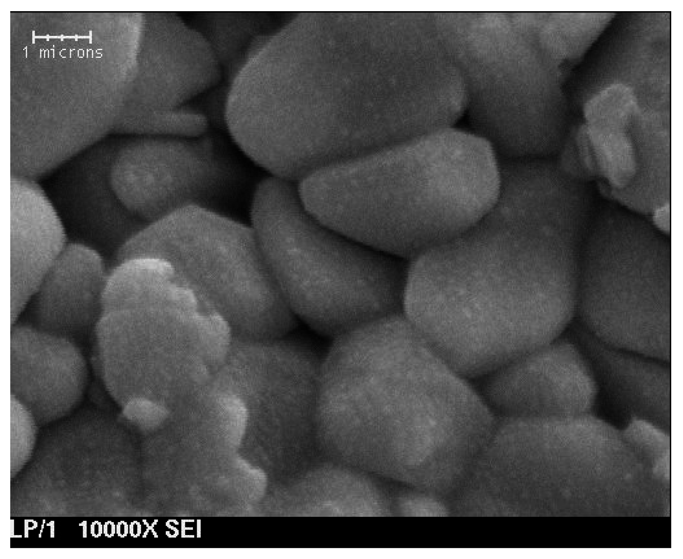
Microstructure of the Thin Films
SEM (scanning electron microscope) has been performed on the thin film samples to examine the structure. The results on the 95%In
2O
3/5%SiO are discussed here.
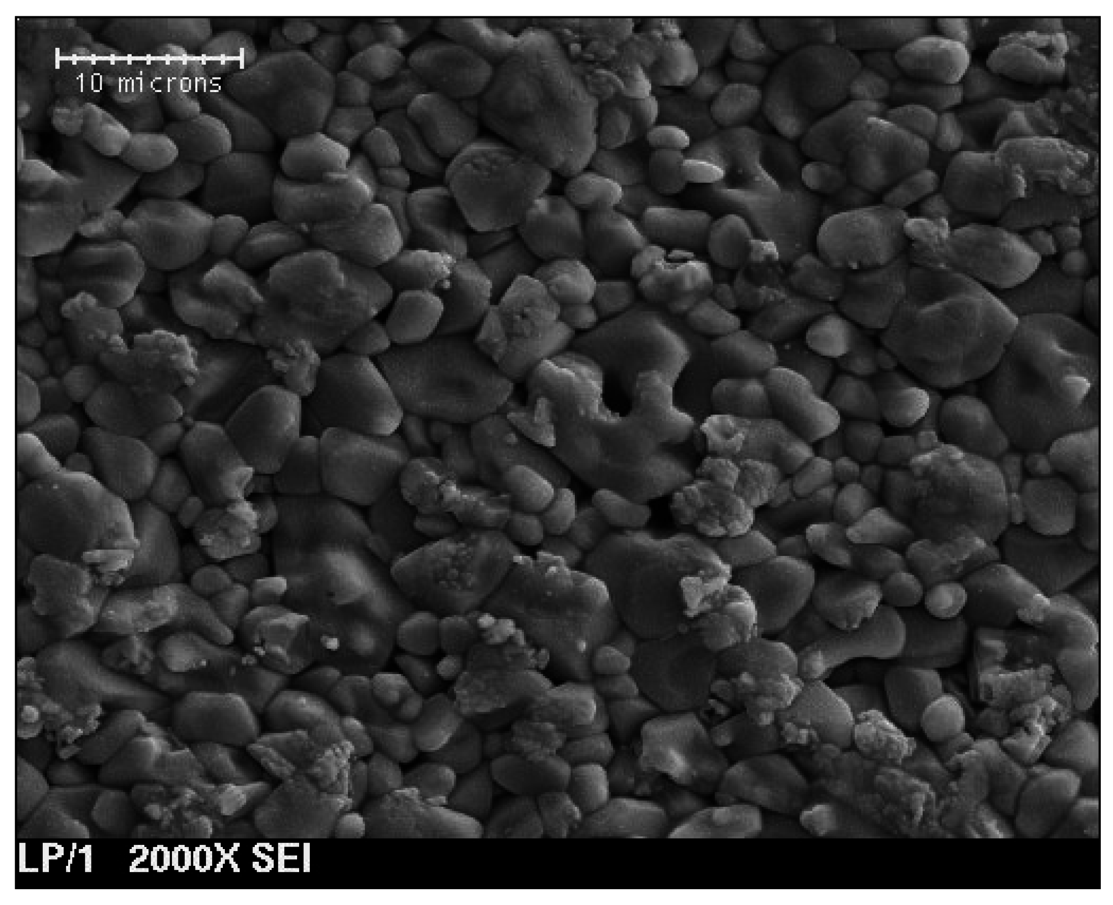
Figure 1 shows the image obtained at a magnification of 2000 and
Figure 2 shows the image obtained at a magnification of 10,000. At a magnification of 2000 the low porosity of the sample can immediately be seen. The particles are close together with relatively few pores between them. Overall it can be said that there is low porosity and the sample appears to be quite dense. At a higher magnification of 10,000, the surface is examined at a much closer range. The separate particles can clearly be seen. However, they are aligned closely together, without any pores separating them. These findings illustrate that the sensing mechanisms in the thin films are probably restricted to a surface-related effect and the bulk has little or no part to play in the conduction mechanisms.
Figure 1.
SEM image of the surface of the In2O3/SiO thin films obtained at a magnification of 2,000.
Figure 1.
SEM image of the surface of the In2O3/SiO thin films obtained at a magnification of 2,000.
Figure 2.
SEM Image of the surface of the In2O3/SiO thin films obtained at a magnification of 10,000.
Figure 2.
SEM Image of the surface of the In2O3/SiO thin films obtained at a magnification of 10,000.
The Sensor Structure and Dimensions
It has been previously mentioned that the conductor is of an interdigitated pattern. Interdigitated structures (IDS) are commonly used as a basis for gas-sensitive layers [
5]. The advantage of sensors based on this structure is the simple and cheap fabrication process and the ability to use the sensor in a wide range of applications without crucial changes to the sensor design [
6]. The IDS is an arrangement of two comb electrodes interlocked into each other. The structure can be considered as many capacitances in parallel sandwiched between the alumina substrate and the sensing film. The sensing layer is deposited over the conductor in a rectangular pattern. The IDS measures an area of 9mm×8mm. Each electrode has a total of 10 interdigits, with each interdigit has a thickness of 0.1mm and a length of 6mm. The space between each interdigit is 0.3mm.
Results
When a new material is investigated for use as a humidity sensor, there will be a number of initial questions, including the mechanisms by which the sensor conducts, the sensitivity of the sensor to humidity and cross-sensitivity to temperature. The following sections deal with the above issues. Firstly, the AC and DC conduction mechanisms are studied. This is followed by an investigation into the temperature response of the samples. Finally, the sensitivity of the samples to humidity is determined.
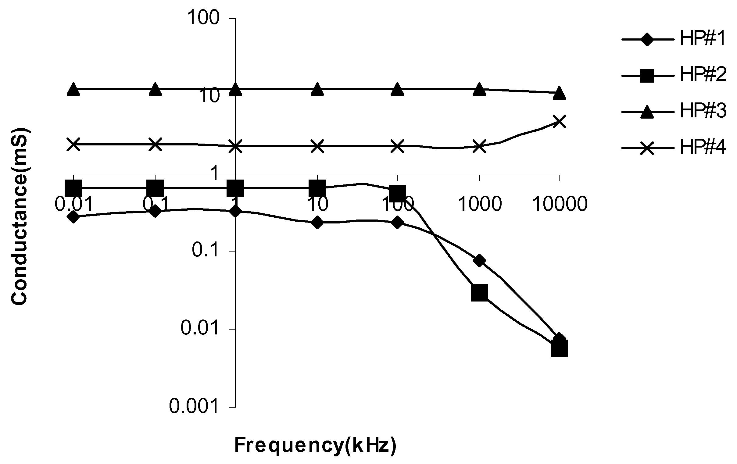
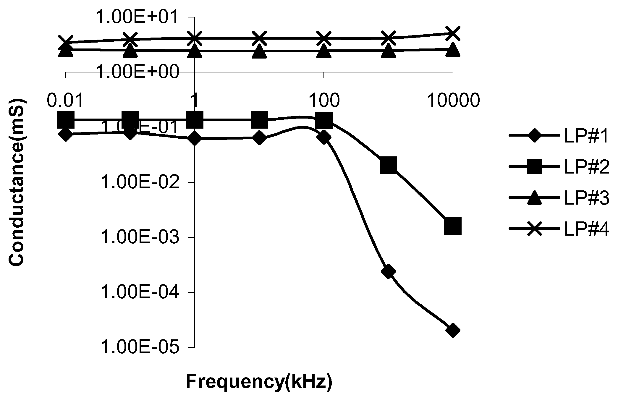
AC Conduction for the In2O3/SiO samples
In
2O
3 thin films having different properties can be prepared by changing factors such as the method of preparation, the substrate temperature, the vacuum pressure etc. The transport properties of thin films strongly depend on their structure (grain size and shape, structural defects etc.) and purity (nature and concentration of the impurities, absorbed and adsorbed gases etc. [
7]. Therefore, it is important to investigate how the transport properties of In
2O
3/SiO films change with different preparative methods. The AC conduction mechanisms of the In
2O
3/SiO samples produced at both low and high vacuum pressure have been studied. The plots of log conductance versus log frequency are shown in
Figure 3 (LP#1-4) and
Figure 4 (HP#1-4).
Figure 3.
The variation of conductance against frequency for the In2O3/SiO samples produced at low vacuum pressure.
Figure 3.
The variation of conductance against frequency for the In2O3/SiO samples produced at low vacuum pressure.
The frequency variation of the ac conductivity component σ
ac may often be approximated by the expression of Pollack and Geballe [
8],
where σ
tot is the total conductivity, A is a constant, ω is the angular frequency and s is an index. The value of the index s can be obtained by evaluating the slope of log σ versus log f curves. According to Pollak and Geballe [
8], if the slope value s is between 0.5 and 1, i.e.
The dominant AC conduction mechanism is hopping of electrons. Values of s outside this range indicate a tunnelling AC conduction mechanism. The s values for the sensor samples have been determined and are tabulated in
Table 2.
Figure 4.
The variation of conductance against frequency for the In2O3/SiO samples produced at high vacuum pressure.
Figure 4.
The variation of conductance against frequency for the In2O3/SiO samples produced at high vacuum pressure.
Table 2.
The s values obtained from log conductance versus log frequency.
Table 2.
The s values obtained from log conductance versus log frequency.
| Sample | S value
0-100kHz | S value
100kHz-10MHz |
|---|
| LP#1 | 0 | 0.61 |
| LP#2 | 0 | 0.95 |
| LP#3 | 0 | 0 |
| LP#4 | 0 | 0.09 |
| HP#1 | 0 | 0.75 |
| HP#2 | 0 | 0.99 |
| HP#3 | 0 | 0 |
| HP#4 | 0 | 0.16 |
Two distinct regions of operation can be identified for the following samples, LP#1,LP#2, HP#1 and HP#2. Region 1, spanning 0-100kHz, indicates tunneling as the dominant AC conduction mechanism (s=0). Region 2, spanning 100kHz-10MHz, indicates hopping as a dominant AC conduction mechanism (0.5<s<1). The hopping conduction mechanism has previously been observedfor In
2O
3 [
9] and CuInSeO
2 [
10]. For the remaining samples, LP#3,4 and HP#3,4, a constant value for s (s=0) indicate that tunneling is the AC conduction mechanism observed over the entire frequency span.
Figure 5.
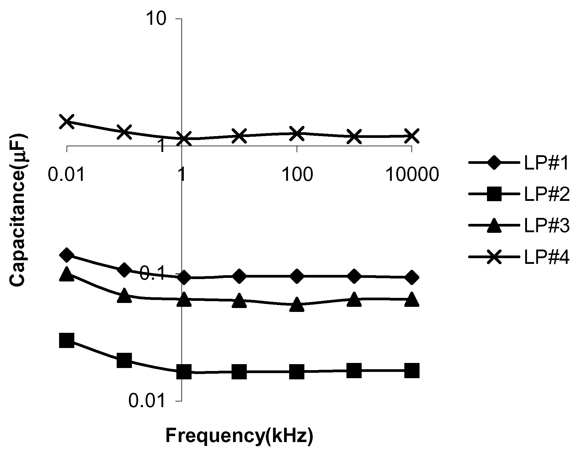
The variation of capacitance against frequency for the In2O3/SiO samples produced at low vacuum pressure.
Figure 5.
The variation of capacitance against frequency for the In2O3/SiO samples produced at low vacuum pressure.
Figure 6.
The variation of capacitance against frequency for the In2O3/SiO samples produced at high vacuum pressure.
Figure 6.
The variation of capacitance against frequency for the In2O3/SiO samples produced at high vacuum pressure.
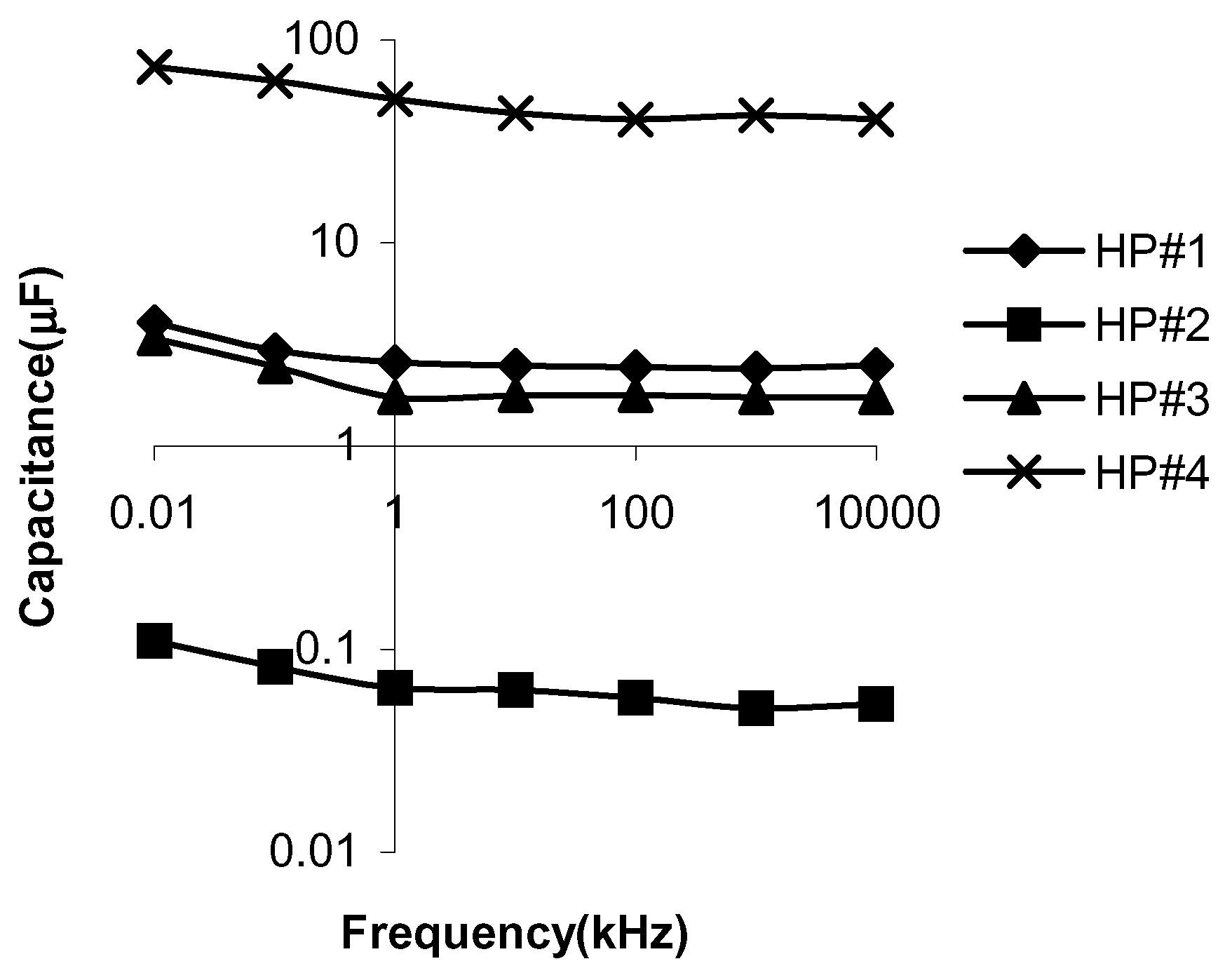
The variation of capacitance against frequency is plotted in
Figure 5 and
Figure 6. It is found that the capacitance decreases as the frequency increases. At higher frequencies (>1kHz) the capacitance remains constant. This behaviour has previously been observed in thin films of copper indium diselenide [
10]. The increase of capacitance with the decrease of frequency in the lower frequency range can be attributed to charge carriers being blocked at the electrodes [
10,
11]. As a result, the carriers become trapped or replaced at the electrodes, resulting in space charge and macroscopic field distortion. This space charge layer should lead to a substantial increase in capacitance [
12,
13,
14].
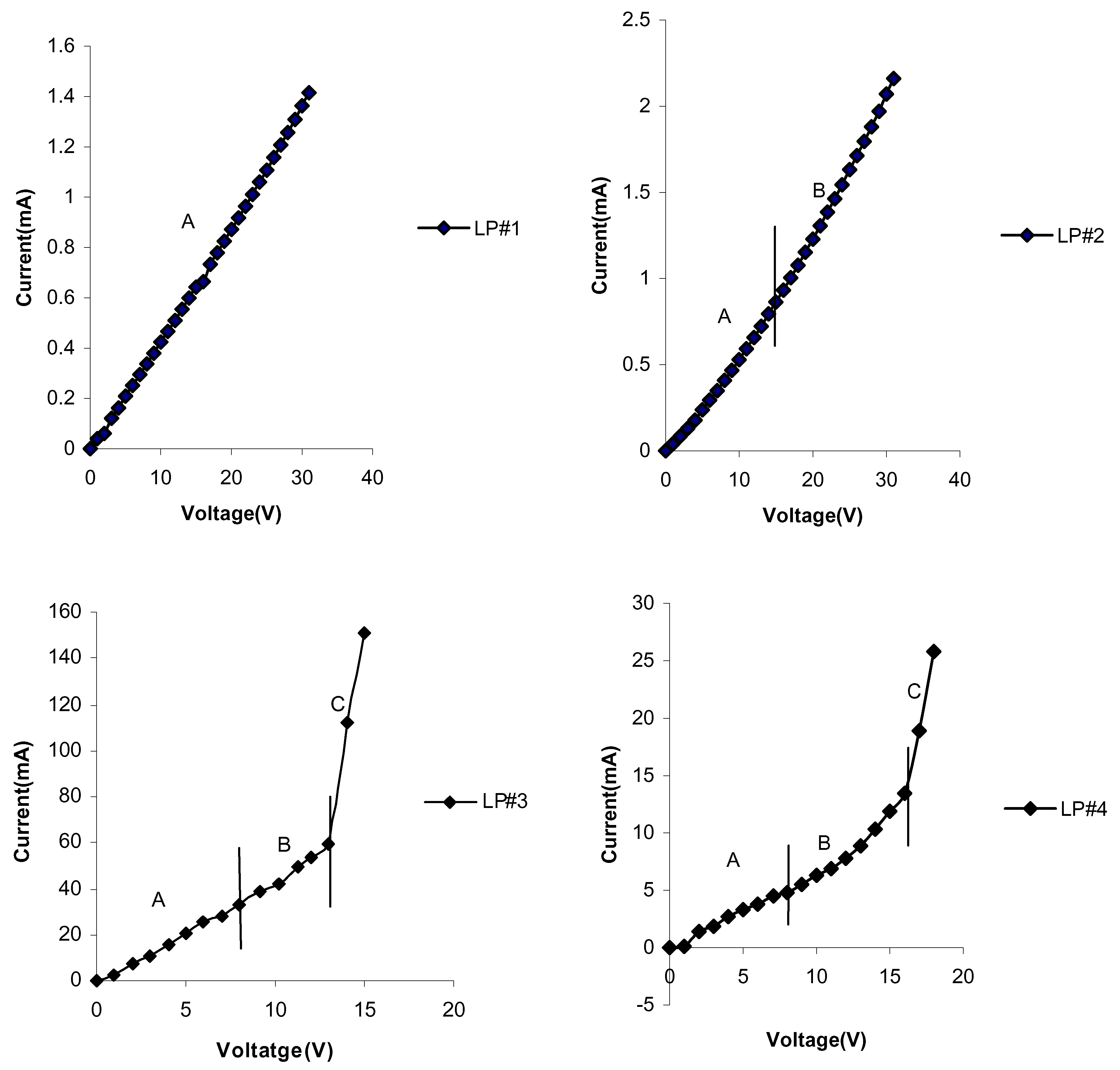
DC Conduction in thin films of In2O3/SiO at low fields
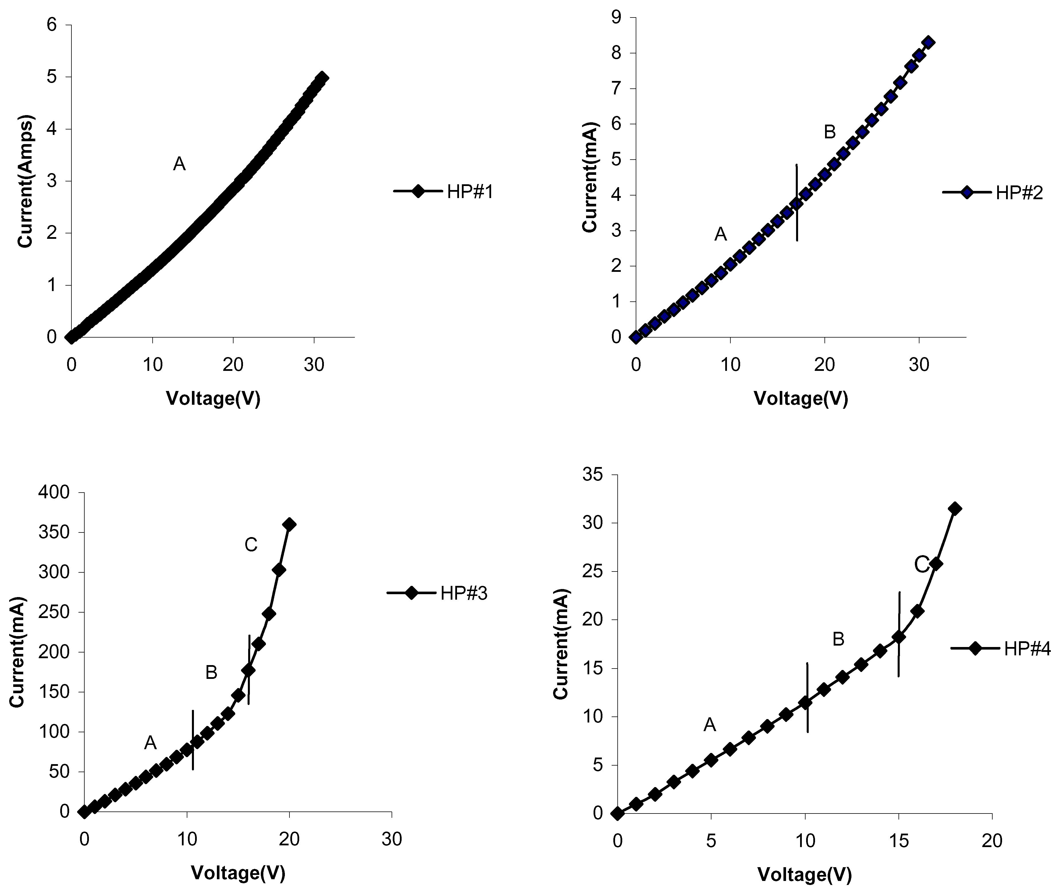
At low-fields thin films usually exhibit an ohmic I-V relationship, i.e. the current is linear to the voltage [
15]. Voltage was applied to the sensor samples and the resulting current was recorded. From the curves, an indication of the DC conduction mechanisms can be obtained. A maximum voltage of 31V was applied to the sensor samples. The results for the low pressure are graphed in
Figure 7. Sample LP#1 shows a linear ohmic I-V relationship over the voltage range 0-31V. LP#2 shows two regions, region A (0-15V): an ohmic region, shows a linear I-V relationship and region B (>15V): a non-ohmic region, shows a non-linear I-V relationship. LP#3 and 4, show three distinct regions of operation, which are indicated on the graphs by A, B and C. These three regions can be observed from the I-V plots of LP#3; region A: 0-8V, is ohmic, B: 8-11V, non-ohmic and C, above 11V, breakaway region, which precedes breakdown. For LP#4 the three regions are as follows: region A: 0-8V, region B: 8-18V and region C: 18V and above. Possibly, three regions of operation could be observed in LP#1,2 is a sufficiently high voltage was applied.
Figure 7.
I-V plots for the In2O3/SiO samples produced at low pressure.
Figure 7.
I-V plots for the In2O3/SiO samples produced at low pressure.
The I-V curves for HP#1-4 are shown in
Figure 8. A maximum voltage of 31V was applied to HP#1 and a linear I-V relationship was observed over the entire voltage range. A voltage of 31V was also applied to HP#2 and two regions of operation were observed. Region A: (0-17V): the ohmic region, shows a linear I-V relationship and region B (>17V): the non-ohmic region, shows a non-linear I-V relationship. One could imagine that a much higher voltage would need to be applied in order to observe a breakdown region in the samples. HP#3 exhibits three regions of operation. Region A (0- 9V): the ohmic region, shows a linear relationship between I and V. Region B (9-14V): the non-ohmic region, shows a non-linear relationship between I and V. Region C (>14V): is the breakaway region. HP#4 also exhibits three regions of operation. Between 0V and 10V, an ohmic region (A) is observed. There is a linear relationship between I and V. From 10V and 14V a non-ohmic region (B) is observed. Finally, a breakaway region (C) is observed at 16V and above.
Figure 8.
I-V plots for the In2O3/SiO samples produced at high pressure.
Figure 8.
I-V plots for the In2O3/SiO samples produced at high pressure.
A general statement can be made governing the I-V plots and the samples; as the In2O3 content decreases the I-V plots change from an overall ohmic relationship, to two distinct regions (Region A: ohmic and Region B: non-ohmic), to three distinct regions (Region A: ohmic, Region B: non-ohmic and Region C: breakaway). The plots where three distinct regions of operation have been observed could be an indication of space charge limited conduction. However, further tests will need to be conducted to ascertain this statement.
Temperature Response
Temperature is a common interfering variable in humidity sensing. Therefore, it is important to determine its effect on the sensors in this study. The samples have been exposed to increasing temperature (293K-423K). Overall, the samples show a resistance decrease with increasing temperature, according to the relationship,
where R is the resistance, R
0 is the initial resistance, Ea is the activation energy and k is Boltzmann’s constant. The temperature response can be given in terms of the relative variation, ΔR, of the sensor resistance to a given temperature,
where R0 is the initial resistance of the sensor and Rt is the resistance at different temperatures. The calibration curves for the samples were obtained by plotting ΔR against the temperatures.
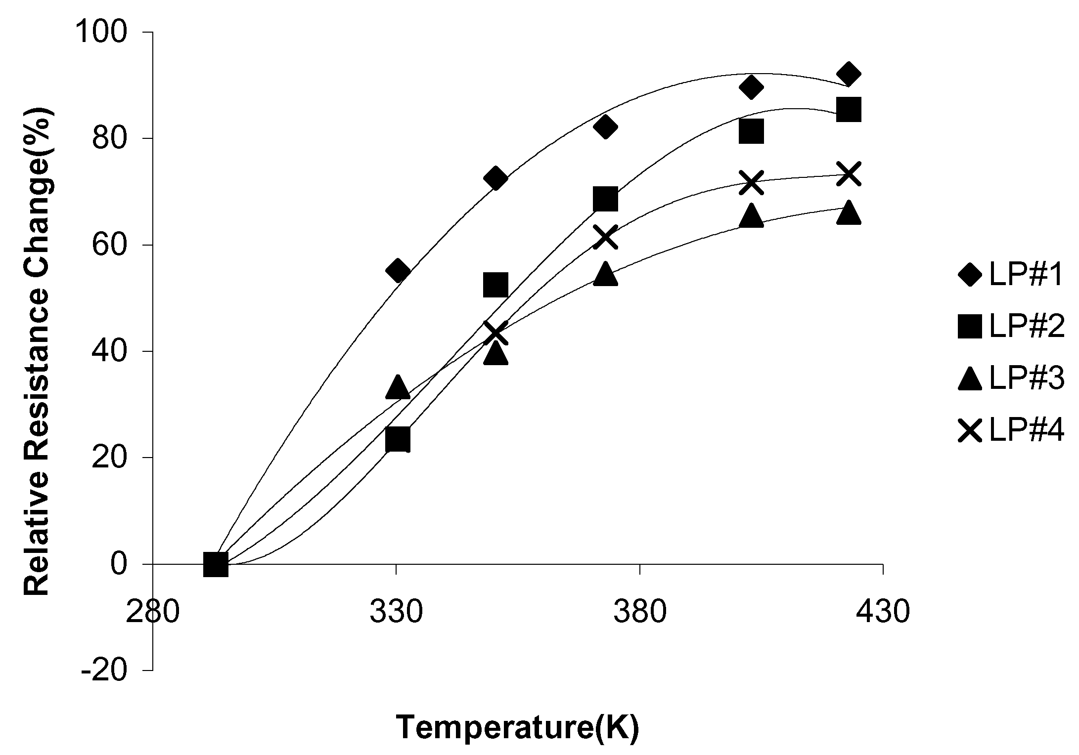
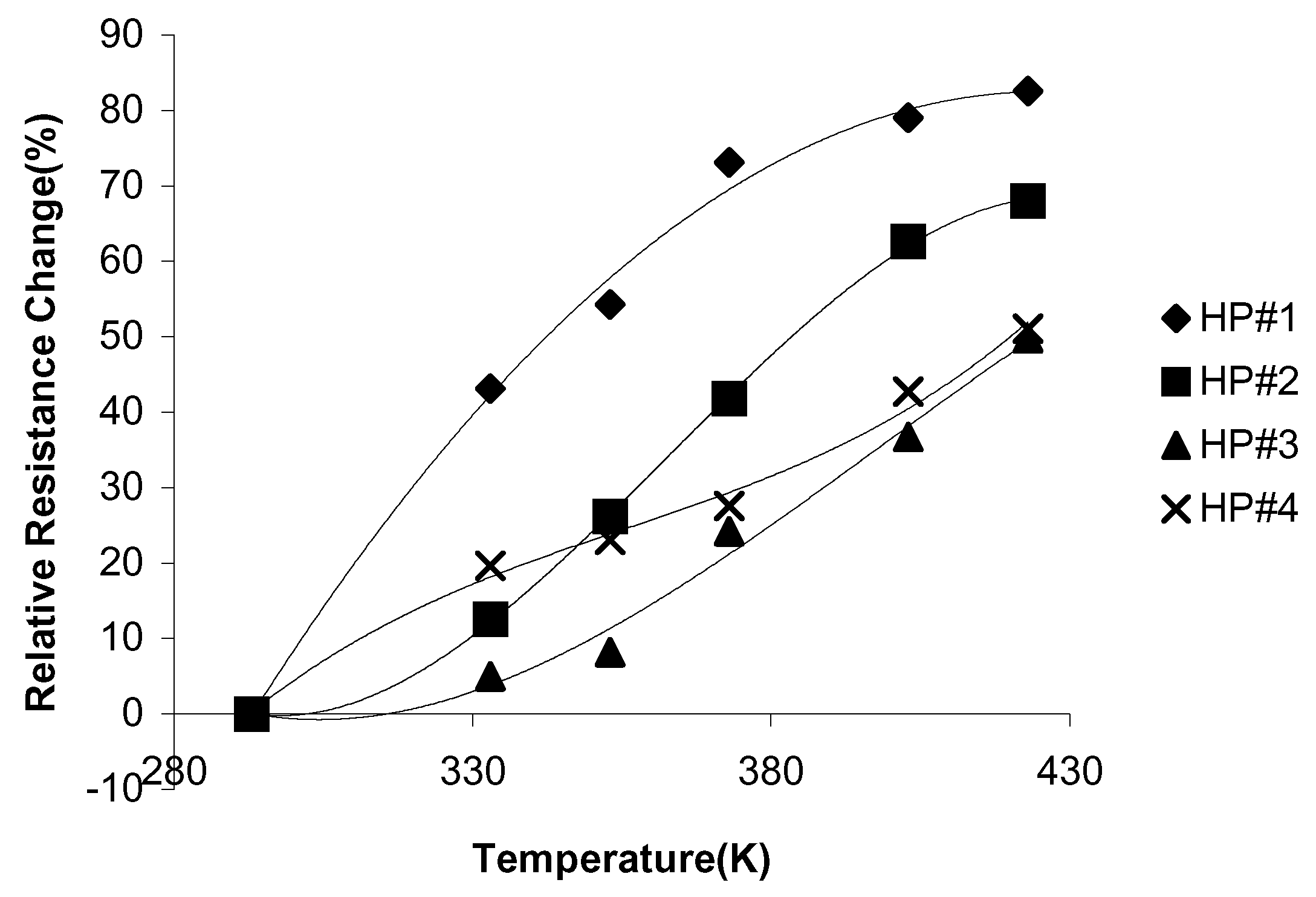
Figure 9 and
Figure 10 show the changes in ΔR against temperature for the low pressure and high pressure samples. The sensitivity of the samples to the temperatures has been determined from the slope of ΔR and is shown in
Table 3.
Figure 9.
The relative resistance change expressed as a percentage against increasing temperature for the In2O3/SiO samples produced at low pressure.
Figure 9.
The relative resistance change expressed as a percentage against increasing temperature for the In2O3/SiO samples produced at low pressure.
For the high pressure samples a decrease in temperature sensitivity is observed with decreasing In2O3. This trend is also observed in the low pressure samples. Therefore, the sensors with the best thermal stability are produced from the 55%In2O3/SiO ratio, at both the high and low vacuum pressures.
Figure 10.
The relative resistance change expressed as a percentage against increasing temperature for the In2O3/SiO samples produced at high pressure.
Figure 10.
The relative resistance change expressed as a percentage against increasing temperature for the In2O3/SiO samples produced at high pressure.
Table 3.
The temperature sensitivity of the sensor samples.
Table 3.
The temperature sensitivity of the sensor samples.
| Sample | Sensitivity(%/K) | Sample | Sensitivity(%/K) |
|---|
| LP#1 | 0.8 | HP#1 | 0.9 |
| LP#2 | 0.6 | HP#2 | 0.7 |
| LP#3 | 0.5 | HP#3 | 0.5 |
| LP#4 | 0.4 | HP#4 | 0.3 |
Humidity Response
To test the humidity sensitivity of the sensors they were exposed to increasing levels of humidity (RH%). The humidity response has been determined in a similar manner to the temperature response,
where R
0 is the initial resistance of the sensor and R
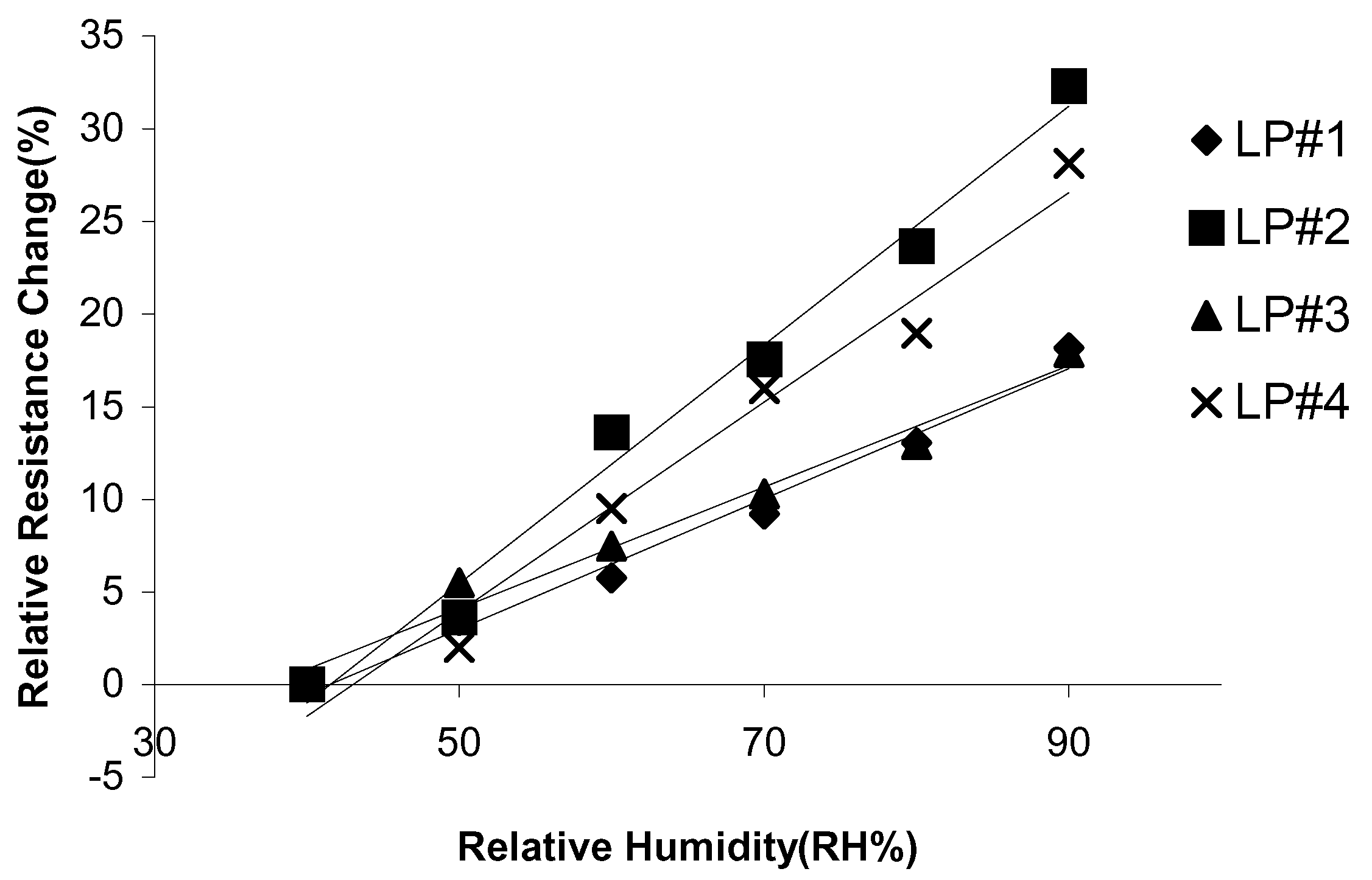
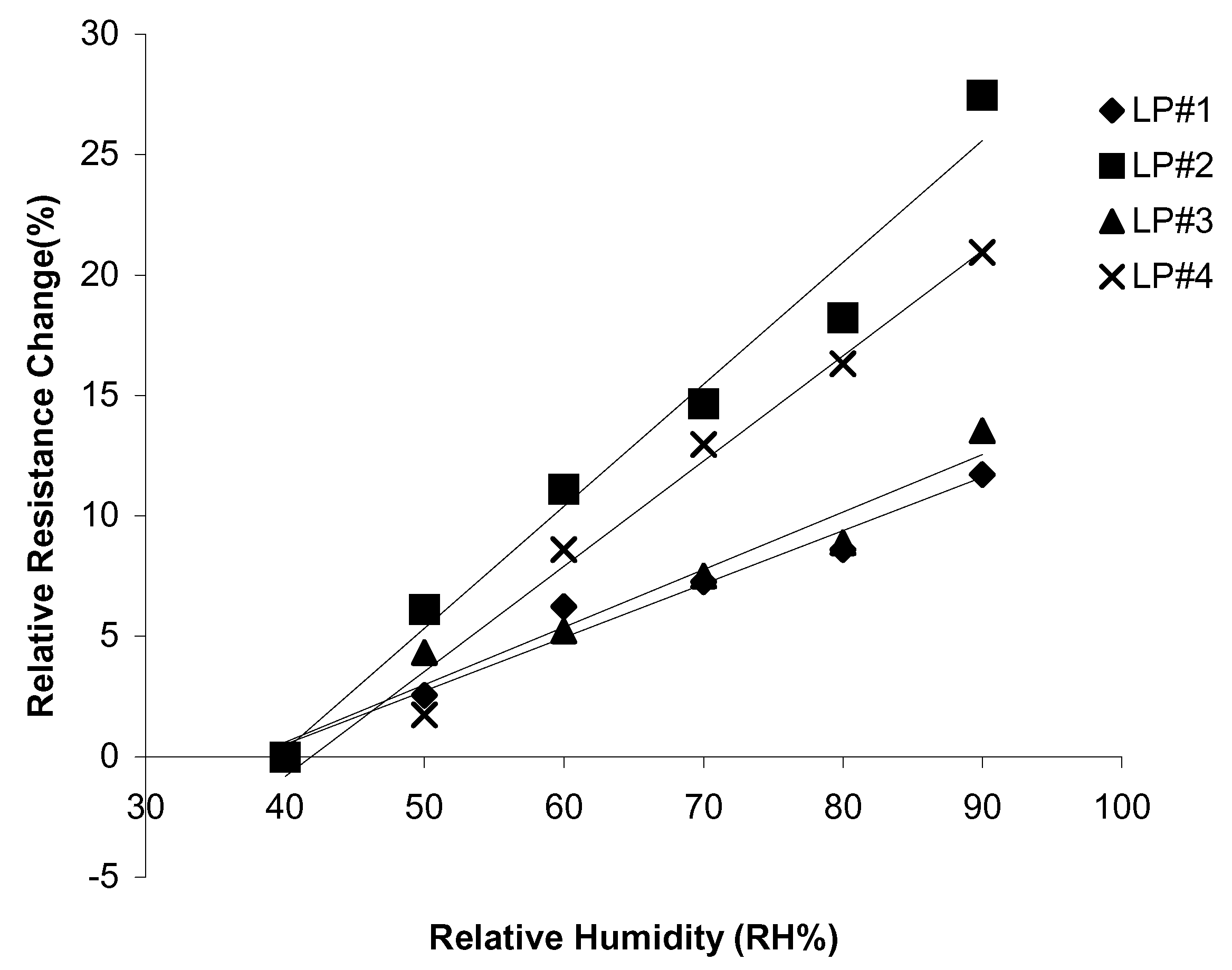
hum is the resistance at different humidity levels. The values of ΔR against RH% for the low pressure samples at 30 and 60°C are plotted in
Figure 11 and
Figure 12. The relative resistance change was recorded over the humidity range 40RH%-90RH% at both 30 and 60°C. The response signals show a good linearity for the given RH% range.
Table 4 lists the humidity sensitivity of each sample at the different operating temperatures. The highest sensitivity is exhibited by LP#2, indicating that the ratio 85%In
2O
3/15%SiO has the greatest potential for use in a humidity sensing application.
Figure 11.
Humidity Sensitivity Curves for In2O3/SiO at 30°C.
Figure 11.
Humidity Sensitivity Curves for In2O3/SiO at 30°C.
Figure 12.
Humidity Sensitivity Curves for In2O3/SiO at 60°C.
Figure 12.
Humidity Sensitivity Curves for In2O3/SiO at 60°C.
Table 4.
Relative humidity (%) sensitivity of each In2O3/SiO sample produced at low pressure, at 30°C and 60°C.
Table 4.
Relative humidity (%) sensitivity of each In2O3/SiO sample produced at low pressure, at 30°C and 60°C.
| Sample | RH% sensitivity at 30°C | RH% sensitivity at 60°C |
|---|
| LP#1 | 0.222%/RH% | 0.352%/RH% |
| LP#2 | 0.506%/RH% | 0.644%/RH% |
| LP#3 | 0.239%/RH% | 0.328%/RH% |
| LP#4 | 0.436%/RH% | 0.566%/RH% |
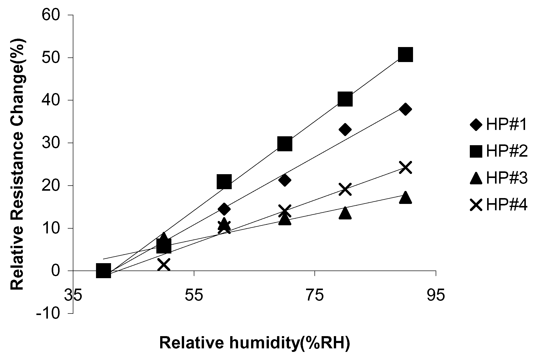
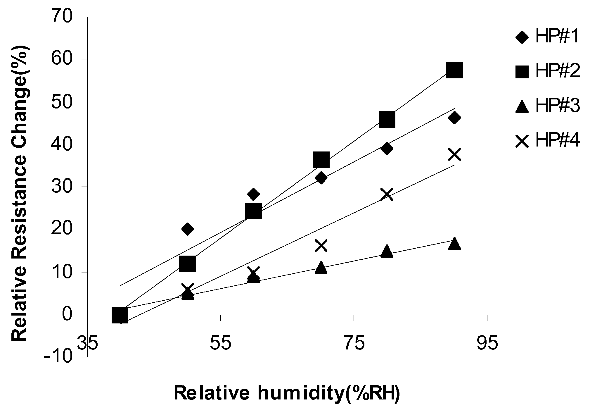
The plots of ΔR against RH% for the high pressure samples at 30 and 60°C are shown in
Figure 13 and
Figure 14. The highest humidity sensitivity is once again observed for the 85%In
2O
3/15%SiO ratio, HP#2. The sensitivities obtained for HP#2, 1.045%/RH% at 30°C, and 1.145%/RH% at 60°C, are higher than the values obtained for LP#2 (0.506 at 30°C, 0.644%/RH% at 60°C). Therefore, the most promising material for humidity sensing appears to be the 85%In
2O
3/15%SiO ratio produced at a vacuum pressure of 2×10⁻⁴ mbar.
Figure 13.
Humidity Sensitivity Curves for In2O3/SiO, produced at high vacuum pressure, at 30°C.
Figure 13.
Humidity Sensitivity Curves for In2O3/SiO, produced at high vacuum pressure, at 30°C.
Figure 14.
Humidity Sensitivity Curves for In2O3/SiO, produced at high vacuum pressure, at 60°C.
Figure 14.
Humidity Sensitivity Curves for In2O3/SiO, produced at high vacuum pressure, at 60°C.
Table 5.
Relative humidity (%) sensitivity of each In2O3/SiO sample, produced at high vacuum pressure, at 30°C and 60°C.
Table 5.
Relative humidity (%) sensitivity of each In2O3/SiO sample, produced at high vacuum pressure, at 30°C and 60°C.
| Sample | RH% sensitivity at 30°C | RH% sensitivity at 60°C |
|---|
| HP#1 | 0.795%/RH% | 0.833%/RH% |
| HP#2 | 1.046%/RH% | 1.145%/RH% |
| HP#3 | 0.3%/RH% | 0.326%/RH% |
| HP#4 | 0.508%/RH% | 0.7532%/RH% |
Mechanism of Water Adsorption for In2O3/SiO thin films
All the sensor samples exhibit a resistance decrease with increasing RH%. Initially, water vapour chemisorbs on the surface of the sensor. The electrical response will depend on the number of water molecules adsorbed on the sensor surface, as seen in spinel thin film humidity sensors [
16]. Water is then physically adsorbed on top of the chemisorbed layer, on-top of which further physisorbed layers will be formed. The physically adsorbed multi-layered water molecules on the surface of the thin sensing film play a dominating role for the humidity sensing mechanism [
17]. It has been reported that conduction in thin films occurs through ionic carriers, while electronic conduction at low RH% is negligible [
16]. The absence of capillary pores makes water condensation, and hence electrolytic conduction, impossible. This results in a thin film humidity sensor having a lower humidity sensitivity than a thick film humidity sensor. However, the advantages to thin films are shorter response time, and a smaller temperature coefficient, due to the lack of condensed water in the pores and the large intrinsic resistance [
17]. The conduction mechanism involved in the water adsorption is related to the surface coverage of water [
18], and is mainly attributed to the hopping mechanism [
2]. The hopping conduction mechanism has been observed in LP#1,2 and HP#1,2, indicating that this mechanism could be responsible for the humidity sensing operations.
Conclusion
An investigation has been conducted into the use of thin films of In2O3/SiO as a humidity sensor. The results have indicated that the ratio 85%In2O3/15%SiO produced at a vacuum pressure of 2×10⁻⁴ mbar shows the best potential for use in a humidity sensing application. A humidity sensitivity of 1.046%/RH%, at temperature of 30°C, and a sensitivity of 1.145%/RH%, at a temperature of 60°C, has been obtained. All the samples have exhibited sensitivity to temperature, with the lowest temperature sensitivity attributed to 55% In2O3/45%SiO ratio. This ratio produced at low vacuum has a temperature sensitivity of 0.4%/K and at high vacuum has a temperature sensitivity of 0.3%/K. In general, two statements can be made concerning the amount of In2O3 in the overall combination of In2O3/SiO: firstly, a decrease in temperature sensitivity is observed with decreasing In2O3, and secondly, as the In2O3 content decreases the regions observed in the I-V plots change from an overall ohmic relationship (region A), to two distinct regions (Region A: ohmic and Region B: non-ohmic), to three distinct regions (Region A: ohmic, Region B: non-ohmic and Region C: breakaway).

