Abstract
Benzene is a carcinogen with a maximum permitted exposure limit in the atmosphere of 16.25µg m-3 (5 ppb). There is a need for an inexpensive instrument for measuring benzene concentrations, particularly in urban areas. We have shown that thin films of titanium dioxide dispersed in poly(vinylidenfluoride) are sensitive to benzene at room temperature with possible applications in benzene monitors. In this paper, we present a detailed study into the direct current electrical characteristics of the films when exposed to benzene. The current I through the films increase linearly with applied voltage, V, at low applied voltages (V ≲0.6V) and at higher voltages, I α V5 The results are consistent with the films being p-type semiconductors and, at higher voltages, the conduction is dominated by a space charge limited process caused by negative traps with an average energy of 0.1 eV. The films are sensitive to benzene only at the higher voltages. The proposed mechanism is that benzene molecules on the surface of the films reduce the concentration of holes. The relative resistance of the films increases linearly (r = 0.92) with benzene concentrations (sensitivity of 0.042% ppm-1) and a detection limit of 10 ppm. The films have response times to increasing and decreasing concentrations of benzene of about 1 and 5 min respectively.
Introduction
Until recently benzene was widely used in industry as a solvent and a cleaning agent. A colourless liquid with a characteristic odour, it is a by-product of many petrochemical processes including oil refining. Benzene is also a carcinogen and is a particular hazard in urban areas as it occurs in the exhaust fumes from motor vehicles. The maximum permitted exposure limit to be achieved by the year 2003 has been set at 16.25 µg m-3 (or 5ppb) when measured as a running mean [1]. Different techniques have been developed to measure atmospheric levels of benzene at these very low concentrations. In the most commonly used technique, samples of the atmosphere taken at the measurement site are pumped into storage bottles and transported to a laboratory for analysis using gas chromatography. Whilst this technique is reliable and accurate, it is also time consuming and expensive. Another technique is based on ultraviolet absorption spectroscopy. The technique requires an optical path length of typically 2 km so is mainly used in large installations, such as oil refineries, and is unsuitable for measurements in confined spaces, such as filling stations [2]. There are also problems with interference from oxygen and ozone [3]. There is a requirement for an inexpensive, hand-held, instrument for the routine measurement of atmospheric concentrations of benzene. Instruments based on thin film devices are becoming popular in these sorts of applications. However, there are no suitable thin films available yet for benzene. Films using the semiconductor titanium dioxide (TiO2) have been reported to be sensitive to different vapours, including benzene, at high temperatures and, or, using alternating currents [4,5]. In a previous paper [6], we showed that thin films of TiO2 could be made sensitive to methanol, ethanol and benzene vapours at room temperature with measurements made using a simple direct current (dc) measuring technique. The films are stable and have a fast response time. We have made a more detailed study into the effect that benzene molecules have on the dc electrical characteristics of the films with a view to improving their sensitivity and these findings are presented in this paper. However, the sensitivity and selectivity of the films are still not good enough to enable them to be used in instruments for the routine monitoring of the very low atmospheric concentrations of benzene.
Experimental
The TiO2 films were prepared by mixing 0.25 mg of TiO2 powder in 2 ml of a solution of N,N-dimethylacetamide containing 0.2 mg of poly(vinylidenfluoride), PVDF. Two gold electrodes (15 × 5 mm) and separated by 1.5 mm were sputtered onto a glass slide. A sensing device was produced by spin coating the TiO2 mixture onto the glass slide so that a thin film covered the two electrodes. Films of different thickness were used in this investigation. The thickness of the TiO2 film was adjusted by varying the concentration of the polymer, the speed of the spin coating and the coating time. An Alpha-Step 200 surface profilometer was used to estimate the thickness of the films. The direct current through the films was measured with a potential difference applied to the electrodes using a Keithley 617 digital electrometer. The films in these investigations were stored and used in the dark at room temperature unless otherwise stated.
The devices were mounted in a specially constructed glass chamber where a carrier gas (nitrogen) containing known concentrations of benzene was passed over the films. The concentration of benzene could be changed rapidly for response time measurements. All the measurements were made under normal atmospheric pressure. The carrier gases with known concentrations of benzene were produced in two stages. In the first stage, nitrogen gas at a flow rate of 100 ml/minute was passed over a permeation vial containing a known quantity of benzene and held at a constant temperature of 25°C. The concentration of the benzene vapour (C1) in the stream of nitrogen with a flow rate of F1 was calculated using [7]:
where P is the permeation rate and ρ is the reciprocal vapour density of the benzene vapour. The concentration of the benzene vapour in the nitrogen stream in this stage was determined to be 500 ppm. In the second stage, the nitrogen flowing from the vial was mixed with a second nitrogen stream and a range of concentrations between 100 and 500 ppm obtained. The resulting concentration was calculated from [7]
where C is the concentration of the measured gas and F2 is the flow rate of the dilution nitrogen stream.
Results and Discussion
DC Electrical Properties of Tio2 Thin Films
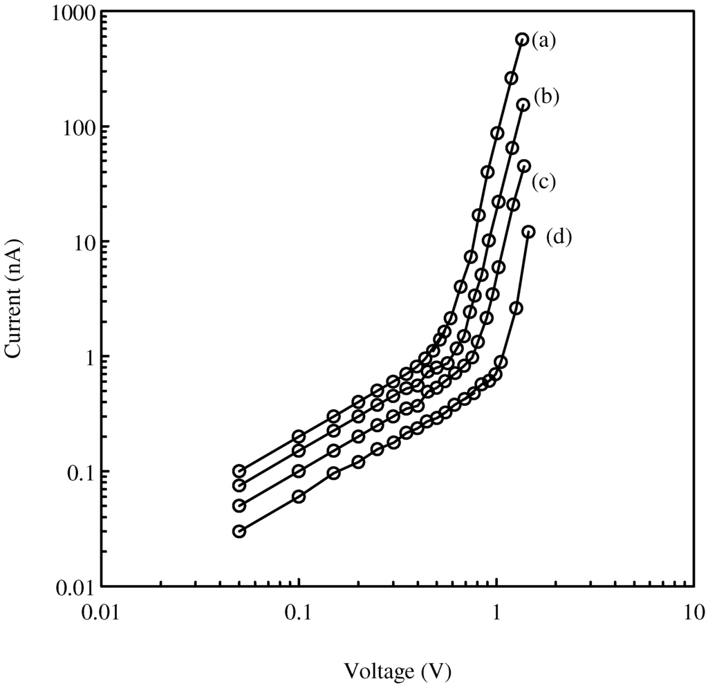
Recordings of the direct current (I) flowing through the TiO2 films over a range of applied voltages (V) were made on several films with different thickness at room temperature and in the open atmosphere of the laboratory. Figure 1 shows the dependence of current I on voltage V for TiO2 films at different thicknesses. Each curve is characterised by two different voltage regions. At lower voltages (less than 0.6 V) the slopes of the curves are approximately unity indicates that ohmic conduction is the main conduction process, whereas at higher voltages the slopes are close to 5 indicates that space charge limited conductivity (SCLC) is responsible for the current through the TiO2 film. The abrupt changes in the slopes of the plots are characteristic of a change in the modes of conduction in the films from Ohmic to space charge limited conductivity (SCLC) [8]. In our previous paper [6], we concluded that the films are p-type semiconductors so the majority carriers are holes. We have shown that oxygen plays a major part in the creation of the holes initially in the valence band of the TiO2 by forming a thin oxide complex layer on the surface of the film.
A hole is formed in the valence band when an electron e– is donated to the complex. At lower applied voltages, the current density is low and the current is given by:
where S is the effective cross-sectional area of the film, p0 is the thermally generated hole concentration in the valence band, e is the electronic charge, μ is the hole mobility and d is the effective film thickness.

Figure 1.
Dependence of current on voltage for TiO2 samples of thicknesses of (a) 5 μm, (b) 10 μm, (c) 15 μm, (d) 20 μm at room temperature.
Thus a graph of logI against logV has a gradient of 1. At higher applied voltages, holes are injected into the films and the current increases rapidly. Mutual repulsion between the holes contributes to the SCLC but the results below show that trap levels play a major part in this case. In p-type semiconductors, the traps are negative and extend in energy from the top of the valence band towards the Fermi level. The mean energy of the traps is kTt, where Tt is a temperature parameter characterising the distribution and k is Boltzmann’s constant. The distribution of trap levels in energy E above the valence band is given by:
where, P(E) is the trap density per unit energy and P0 is the value of P(E) at the valence band edge. The current-voltage dependence in this case is given by [8]:
 where, NV is the effective density of states in the valence band, ε is the permittivity, and ℓ = Tt/T (T is the temperature of the film). It follows from equation (6) that in the SCLC region, I ∝ Vℓ+1. Taking the logarithm of equation (6):

log I = log [Seμ NV {ε/(eP0kTt)}ℓ] - (2ℓ + 1) · log d + (ℓ + 1) · logV
Thus in the SCLC region, a graph of logI against logV will have a slope of (ℓ +1) for a film with a particular thickness. From Figure 1, the slopes of the line in the SCLC region ≈ 5 so that ℓ ≈ 4. The characteristic temperature Tt ≈ 1200 K at room temperature (T = 300 K) and the mean trap energy kTt ≈ 0.1eV. The power law relationship between I and V in the SCLC region is I ∝ V5. This result indicates that traps in the film are the main contributors to the SCLC region. If traps are not present then the SCLC is dominated by mutual repulsion between the charge carriers and the expected power law relationship between I and V is I ∝ V2 (Child-Langmuir Law).

Figure 2.
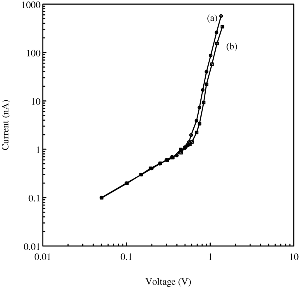
Current-voltage characteristics of a fresh TiO2 film of thickness 5 μm exposed to (a) nitrogen, (b) 150 ppm benzene at room temperature.
The dc Electrical Properties of the Films in the Presence of Benzene
The electrical characteristics of the TiO2 films were investigated when exposed to an atmosphere containing 150 ppm of benzene vapour in nitrogen at room temperature. The measurements were performed on several films containing different amounts of TiO2 and PVDF and with different thickness. The films exhibit similar reversible and reproducible changes in their characteristics when exposed to benzene and a typical response is shown in Figure 2. The presence of the benzene causes the resistance of the films to increase but only in the part of the electrical characteristics where the applied voltage V is greater than 0.6V. From the previous investigations, this suggests that the benzene only affects the SCLC region of the characteristic and has negligible effect on the Ohmic conduction region. In the following experiments, the response of the films to different concentrations of benzene was determined and the films were operated in the SCLC region.
The Response of the Films to Different Concentrations of Benzene
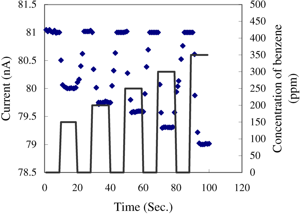
Measurements on the response of the films to benzene were made using freshly prepared TiO2 films. The direct current through films with a thickness of 5 μm was measured at V = 1V as the concentration of the benzene vapour in the nitrogen carrier gas was increased and decreased in steps of 50 ppm over the range 150 ppm to 350 ppm. After each increase in concentration of the benzene, the glass sample chamber was flushed with nitrogen. In all cases, the current through the films decreased as the concentration of the benzene in the carrier gases increased (Figure 3). The films have fast response times to increasing and decreasing concentrations of benzene (about 1 min and 5 min respectively).

Figure 3.
Variation of the current flowing through a fresh TiO2 sensor when exposed to step changes in the concentration of benzene at room temperature.
The response of a p-type semiconductor sensor to reducing gases can be expressed in terms of the relative variation, ∆R, of the sensor resistance to a given concentration of the vapour [9].
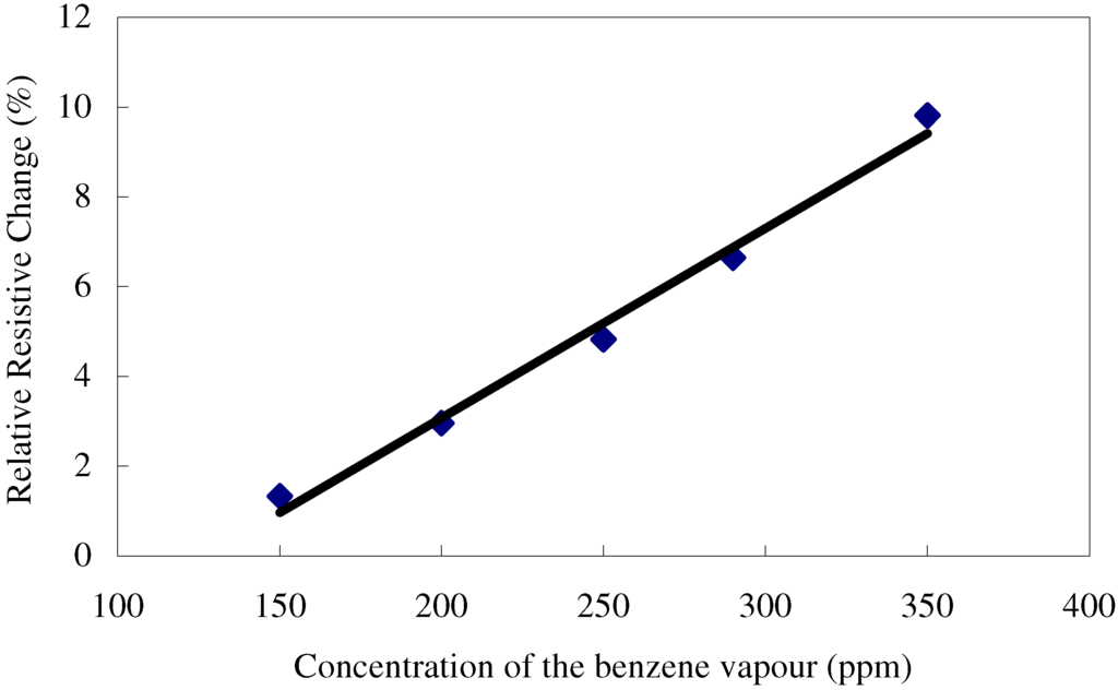
where, Rvapour is the resistance of the film when exposed to an atmosphere containing a known concentration of the vapour and R0 is the resistance of the film when exposed just to the carrier gas. The calibration curve for a film was obtained by plotting ∆R against the concentration of benzene vapour in the carrier gas (Figure 4). The relative resistance of the sensor increased linearly with increasing concentrations of benzene (r = 0.92) over the range 150 to 350 ppm. The sensitivity of the films to benzene (0.042% ppm-1) was determined from the slope of the graph. The detection limit for the benzene vapours is about 10 ppm. All films tested have a similar response to benzene but thinner films are generally more sensitive and have a more linear response. These results indicate that it should be possible to make a film suitable for the routine analysis of atmospheric concentrations of benzene (detection limit <5 ppm) simply by making the films very much thinner. However, it was not possible to make reliable films thinner than 5µm using the simple spin coating technique.

Figure 4.
Variation in relative resistance ∆R of a fresh TiO2 sensor as a function of the concentration of benzene in the carrier gas.
Proposed Mechanism for the Detection of Benzene
The fast response and recovery times of the films to benzene implies that the benzene vapour molecules must interact weakly and reversibly with the TiO2 films. Thinner TiO2 films are more sensitive to benzene than thicker ones so it is likely that the adsorbed benzene molecules have a surface, rather than a bulk effect on the conduction characteristics of the films. Just a few molecular layers below the surface of the film are probably affected by the interaction. The films are operated in the SCLC region of their characteristics where they are p-type semiconductors. The benzene molecules on the surface must interact with the holes causing the resistance of the films to increase by producing more traps in the film, or by injecting electrons into the valence band, or both. It is more likely that the interaction results in electrons being injected into the valence band, as this process is probably more rapid and readily reversible than the creation of traps. A proposed mechanism involves the production of surface donor states in the film by the benzene. The first stage of the process is the formation of a weak complex between benzene molecules and the surface of the film.
C6H6 + TiO2 ⇄ C6H6 -TiO2
The complex then ionises and donor states are produced in the surface molecular layers of the film.
C6H6 -TiO2 ⇄ C6H6+ + TiO2 -
Initially, these donor states lie below the Fermi energy level so that ionisation of the donor states proceeds rapidly and electrons are released into the valence band.
TiO2 - ⇄ TiO2 + e-
As more surface donor states are ionised, the Fermi energy level shifts away from the valence band and the process slows down. Eventually, the Fermi level stops at some new energy value as a dynamic equilibrium is set up between benzene molecules diffusing out of the film to rejoin the ambient atmosphere and molecules diffusing into the film. The electrons injected into the valence band combine with holes, thus reducing the number of charge carriers and increasing the resistance of the film. Decreasing the concentration of benzene in the ambient atmosphere reverses the process and a new equilibrium is established. Consequently, the number of surface donor states created by the benzene molecules adsorbed onto the film surface decreases and the Fermi energy level moves back towards the valence band, resulting in an increase in the current through the film. The overall efficiency of the above reactions is likely to be very low accounting for the relatively poor sensitivity of the films to benzene.
Conclusions
Thin films containing TiO2 dispersed in poly(vinylidenfluoride) are sensitive to benzene vapour at room temperature when the applied voltage is greater than 0.6V dc. In this region, the films behave as p-type semiconductors and the characteristics are dominated by a space charge limiting conductivity process. A proposed mechanism for the sensitivity of the films to benzene involves the creation of surface donor states. The relative resistance of the films increases linearly (r = 0.92) to increasing benzene concentrations with a sensitivity of 0.042% ppm-1 and a detection limit of 10 ppm. The detection limit of the films to benzene has to be improved much further if they are to be used in instruments that meet the requirements of the current legislation on the maximum exposure limits to atmospheric concentrations of benzene.
References
- The Air Quality Strategy for England, Scotland, Wales and Northern Ireland. A Consultation Document, Chapter 4 Section 12, Department of the Environment, Transport and the Regions, London, 25 August 1999 (updated 19 January 2000).
- Trost, B.; Stutz, J.; Platt, U. Atmosph. Env. 1997, 31, 3999–4008.
- Volkamer, R.; Etzkorn, T.; Geyer, A.; Platt, U. Atmosph. Env. 1998, 32, 3731–3747.
- Islam, M.R.; Kumazawa, N.; Takeuchi, M. Appl. Surf. Sci. 1999, 142, 262–266. [CrossRef]
- Garzella, C.; Comini, E.; Tempesti, E.; Frigeri, C.; Sberveglieri, G. Sensors and Actuators B 2000, 68, 189–196.
- Mabrook, M.; Hawkins, P. Sensors and Actuators B 2001, 75, 197–202.
- Namiesik, J.J. Chromatogr. 1984, 300, 79–108.
- Lampert, M.A.; Mark, P. Current injection in solids; Academic Press: New York, 1970; Chapter 2; pp. 15–30. [Google Scholar]
- Yamada, Y.; Seno, Y.; Masuoka, Y.; nakamura, T.; Yamashita, K. Sensors and Actuators B 2000, 66, 164–166.
- Sample Availability: Available from the author.
© 2002 by MDPI (http://www.mdpi.net). Reproduction is permitted for noncommercial purposes.