Low Power CMOS-Based Hall Sensor with Simple Structure Using Double-Sampling Delta-Sigma ADC

1
Department of Electrical and Electronic Engineering, Konkuk University, Seoul 05029, Korea
2
Department of Electrical and Electronic Engineering, Kookmin University, Seoul 02707, Korea
*
Author to whom correspondence should be addressed.
Sensors 2020, 20(18), 5285; https://doi.org/10.3390/s20185285
Submission received: 3 August 2020
/
Revised: 11 September 2020
/
Accepted: 11 September 2020
/
Published: 16 September 2020
(This article belongs to the Section Electronic Sensors)
Abstract
:A CMOS (Complementary metal-oxide-semiconductor) Hall sensor with low power consumption and simple structure is introduced. The tiny magnetic signal from Hall device could be detected by a high-resolution delta-sigma ADC in presence of offset and flickering noise. Also, the offset as well as the flickering noise are effectively suppressed by the current spinning technique combined with double sampling switches of the ADC. The double sampling scheme of the ADC reduces the operating frequency and helps to reduce the power consumption. The prototype Hall sensor is fabricated in a 0.18-µm CMOS process, and the measurement shows detection range of ±150 mT and sensitivity of 110 µV/mT. The size of active area is 0.7 mm2, and the total power consumption is 4.9 mW. The proposed system is advantageous not only for low power consumption, but also for small sensor size due to its simplicity.

1. Introduction
A Hall sensor is used in various applications such as magnetic field measurement, automotive industry, consumer electronic products, etc. [1,2]. When a magnetic field is applied in the direction perpendicular to the moving direction of electric charges flowing in a conductor or semiconductor, Lorentz force is generated in the direction perpendicular to the direction of the electric charge movement. This phenomenon is known as Hall effect and the resulting output signal in type of either voltage or current is called Hall signal. A Hall sensor is a kind of magnetic sensor utilizing the aforementioned Hall signal, and the key component of a Hall sensor that converts an external magnetic field into voltage or current output signal is a Hall device. A Hall sensor consisting of a Hall device and other read-out circuits can be fabricated on semiconductor material including bipolar or CMOS (Complementary metal-oxide-semiconductor) processes. In particular, a CMOS-based Hall sensor is widely used due to the advantages of small size, low cost, and high reliability, etc. [3,4]. However, the Hall device in a CMOS process often suffers from offset and sensitivity problems. Large offset occurs due to process non-idealities, such as local difference in doping concentration, hole electrode asymmetry, package stress, and other process-voltage-temperature (PVT) variations, and it interferes with the detection of small input signals. Another shortcoming of a CMOS Hall device is low sensitivity which is mainly affected by the material characteristic and it leads to weak output signal. Commercial CMOS processes do not give designers the freedom to choose materials, so instead, sensitivity is generally enhanced by modifying the Hall device shape. Various Hall device structures such as four contact (4F) or multiple-terminal ones [5,6,7] have been attempted, but the improvement is not significant due to limitation on the material used. Therefore, the amplification process in a Hall sensor is essential to achieve a high signal-to-noise ratio (SNR), and a low-noise operational amplifier (op-amp) is very often used in the system. However, an op-amp in a CMOS process suffers from the trade-off between noise and power consumption, and the performance of an op-amp is vulnerable to PVT variation. The bigger difficulty with amplification is that the gain can be limited due to the large offset. This must be handled using a filter at expense of additional power consumption and hardware size.
A conventional Hall sensor system that overcomes sensitivity and offset problems is shown in Figure 1. An external magnetic field generates a Hall signal (SHALL), and the current spinning technique [6,8] is applied to a Hall device to separate SHALL from offset and flickering (1/f) noise (from the Hall device) on the frequency domain, e.g., offset and 1/f noise at DC and SHALL at chopping frequency fCH. SHALL usually goes to a higher frequency region to minimize the effect of 1/f noise arising from the following blocks. Then, SHALL as well as offset and 1/f noise are amplified by a gain of G and their positions in the frequency domain are switched by a chopper. Finally, the undesired components at fCH are attenuated by a low pass filter and the following analog-digital converter digitalizes only the input related signal. Although this conventional configuration is effective for achieving high SNR by suppressing offset and 1/f noise, its circuit implementation is very complex and the hardware size as well as power consumption increase significantly. Furthermore, the addition of other high-resolution techniques such as auto-zero technique, correlated double sampling, or switched biasing amplifier will make things worse [9,10,11,12].
In this work, we propose a new Hall sensor system architecture consisting of only a Hall device and a high-resolution double sampling discrete-time delta-sigma ADC. The Hall sensor system can be extremely simplified by handling the small Hall signal (SHALL) directly with a high-resolution ADC with inherit chopper stabilization. As in Figure 2, SHALL is located around DC while the offset and 1/f noise are translated to higher frequency by choosing a different current spinning direction to that shown in Figure 1. Then, the weak SHALL can be detected by a noise-shaping ADC regardless of the existence of the offset and 1/f noise, which can significantly reduce circuit complexity, area, and power consumption.
2. Proposed Hall Sensor Architecture
2.1. Hall Device Structure and Current Spinning
There are two types of Hall devices depending on the signal direction: a horizontal type Hall device (HHD) and a vertical type Hall device (VHD), and Figure 3 shows popular structures of an HHD and a VHD. In case of an HHD in Figure 3a, the magnetic field is applied in the vertical direction to P-substrate and the Hall signal shows as voltage output VHALL, which is called Hall voltage and formed in the vertical direction to the magnetic field. For a VHD, the magnetic field is applied in the horizontal direction to P-substrate as in Figure 3b, and the Hall signal is formed in current type (IHALL). Due to the short circuit effect, the sensitivity of VHDs is usually lower than that of HHDs [5,7], so an HHD is used in this work to achieve high sensitivity. Many HHD structures are introduced so far, and among them, we use a cross-sectional structure since it is the most optimized one for the sensitivity [13,14].
However, the cross-sectional HHD suffers from an offset problem like other kinds of Hall devices due to process non-idealities. There are several circuit techniques removing offset of a Hall device, and the current spinning technique is the most widely used one due to its high efficiency. The current spinning technique models a Hall device with a Wheatstone bridge circuit consisting of four resistors (R). When the Hall device is ideal, all resistors have the same resistance and no offset occurs. Also, due to the perfect symmetry, the Hall voltage (VHALL) would be the same regardless of the current direction as in Figure 4. If there is any asymmetry in a Hall device caused by non-idealities, the four-resistor model will have different resistances and it can be modeled with a small resistance (∆R) as in Figure 5. This difference generates offset voltage at the output, but it can be cancelled out by switching the current direction. The offset voltage alternates its polarity depending on the current direction as in Figure 5 while VHALL remains the same as mentioned above. Therefore, periodic change of the current direction modulates only the offset voltage(+/−VOFFSET) and translates it from DC to high frequency band. At the same time, the current spinning is also applied to 1/f noise from the Hall device, which moves to high frequency band along with the offset. This allows for the isolation of unwanted signals. However, VOFFSET is often larger than VHALL, so complicated signal processing may be necessary after the isolation.
2.2. Directly Connected Hall Device and High-Resolution Discrete-Time Delta-Sigma ADC
A conventional Hall sensor requires many blocks to remove the offset and 1/f noise, which increases power consumption, chip area, and design complexity. To mitigate the problem, we propose a simple Hall sensor architecture composed of only a Hall device and an ADC avoiding the use of many complicated signal processing blocks such as an amplifier and a filter. However, if a Nyquist rate ADC is used as in a conventional Hall sensor system, even though the offset and 1/f noise are isolated by current spinning, an ADC with a very high-resolution is necessary to detect the small Hall voltage, which can make things worse since the power consumption increases four times faster than the resolution. A delta-sigma ADC can be a good option since it can digitize only the Hall voltage with high-resolution (more than 15-bits) with the help of oversampling and noise shaping [15,16,17]. A Hall device and a delta-sigma ADC can be easily combined keeping the current spinning capability. By spinning the bias current direction according to the sampling frequency of a discrete-time delta-sigma ADC, the offset and 1/f noise are moved to the Nyquist frequency while the Hall voltage stays within the band of the ADC. The proposed system and operation timing diagram are shown in Figure 6. The ADC samples the Hall voltage on Cs during half of the sampling period (Phase ϕ1), and the sampled signal is processed by the first integrator for the next half of the period (Phase ϕ2). The first integrator output is passed to the next stages sequentially, and the final digital output (DOUT) is obtained at the comparator every sampling clock period. For current spinning, the Hall device changes its connection (ϕ1A, ϕ1B) every sampling clock period as in Figure 6, and the sampling switches (SSPA, SSPB) at the ADC input are turned on and off accordingly. Then, the sampled input signal is integrated by common integration switches (SINT). This configuration is advantageous to achieve high SNR as long as the oversampling ratio is high enough to prevent noise folding problem. However, for a given signal bandwidth and SNR, the increase of oversampling ratio will increase the power consumption of a delta-sigma ADC, and the total power saving might not be substantial compared to a conventional Hall sensor system.
2.3. Double Sampling Delta-Sigma ADC
In the proposed Hall sensor system above, the power consumption is now dominated by the high-resolution delta-sigma ADC with a high oversampling ratio. For a given signal bandwidth, increasing the oversampling ratio requires a very high sampling frequency, resulting in high power consumption due to discrete-time operation. Therefore, the ADC operation speed should be optimized to achieve good power efficiency of the whole system, and a very effective but simple solution is using double sampling scheme [18]. In a double sampling system, the input is sampled at every phase of the sampling clock, and the sampling frequency becomes doubled compared to that with conventional sampling. In other words, the sampling clock speed could be halved for a given signal bandwidth, and the power consumption can be reduced substantially as well. Speed of a discrete-time delta-sigma ADC is mostly limited by the settling time of an integrator that dominates the whole power consumption, and effectively doubled settling time of integrators is allowed in the double sampling scheme. Therefore, a double sampling delta-sigma ADC is often used in sensor applications where high-resolution and low power consumption are critical [19,20]. The proposed double sampling Hall sensor system and its operation timing diagram are shown in Figure 7. The ADC includes two sets of track-and-hold (T/H) circuits, and in Phase ϕ1, the Hall voltage is sampled on CSA while the previously sampled signal on CSB is integrated by the first integrator. In the next phase (Phase ϕ2), CSB now samples the Hall voltage, and at the same time, the signal on CSA gets integrated. This parallel sampling-integration process by the two T/H circuits is repeated, and the first integrator output is passed to the next integrator every half clock phase (TS/2). After the sequential operation, the final digital output (DOUT) is obtained at the comparator output which runs at the speed of 2fS. In addition to the advantage of speed increase (or power saving), the current spinning becomes even easier in the proposed system due to the two T/H circuits. The two sets of outputs of the Hall device only need to be each connected to the sampling switches (SSPA, SSPB), and no additional circuitry is necessary to isolate the offset and noise. Therefore, the proposed Hall sensor system architecture not only reduces the power consumption, but also substantially simplifies the hardware implementation.
3. Circuit Implementation
3.1. Cross-Sectional Horizontal Hall Device
A cross-sectional HHD is chosen as mentioned in Section 2.1 due to its relatively high sensitivity compared to other structures, and it is designed in a CMOS process. Although the HHD’s offset can be eliminated by current spinning technique, it still exists at the HHD’s output and limits the input range of a high-resolution delta-sigma ADC. Therefore, the layout is carefully optimized to minimize the offset and maximize the sensor dynamic range. A perfectly symmetrical cross-shaped Hall device is surrounded by a wide guard ring to minimize external influences on the offset as shown in Figure 8. The Hall device itself is made of N-well layer on P-substrate and has a size of 100 × 100 µm optimized for offset [13,14]. There are 4 terminals based on N+ doping for current spinning of the Hall device, and the length of metal wires connected to the terminals as well as switches are also balanced.
3.2. 3rd-Order Discrete-Time Delta-Sigma ADC
A 3rd-order discrete-time delta-sigma ADC is used in the proposed system to achieve more than 15-bit resolution, and the structure is shown in Figure 7 and Figure 9. It has CIFF structure for low power consumption and high linearity [21]. There are three integrators for 3rd-order noise shaping and the quantizer performs 1bit quantization. The integrator and DAC coefficients are optimized for high dynamic range and for easy signal summation before the quantization, and the resulting noise transfer function of the ADC is as Equation (1).
The three poles are located at (0.5822 + j0), (0.934 − j0.2792), (0.934 + j0.2792) in pole-zero plot, and they are all inside the unit circle and the stability is ensured. The simulation shows an SNDR of 92 dB when the oversampling ratio is 128.
The integrators are based on switched-capacitor amplifiers, and the circuit implementation of the amplifier is shown in Figure 10. Requirement for the amplifier is very high due to the target resolution, and a pseudo differential amplifier consisting of inverters is used instead of a conventional operational amplifier which is often energy inefficient [22,23,24,25]. The pseudo differential amplifier has a very simple structure and has two complementary source-coupled pairs for low power consumption. The gain of the amplifier can be derived as Equation (2).
where gmn1,2 and gmp1,2 represent the transconductance of the complementary input devices (MN1,2 and MP1,2) respectively, and ron1,2 and rop1,2 represent the output resistance of them. The input devices have length of >10 µm to achieve DC gain over 60 dB in a typical condition that is enough for the ADC target performance. Figure 10 shows the input referred noise curve of the amplifier, and the integrated input referred noise from 100 Hz to 7.81 KHz is simulated to be 5.24 µVrms, which corresponds to 0.508 µT in our system. Therefore, noise from the amplifier is low enough not to affect the overall system resolution, and the thermal noise from the Hall device becomes the main noise source.
Gain = (gmn1,2 + gmp1,2)(ron1,2//rop1,2)
The common mode feedback circuit consists of switched capacitors as conventional ones [26]. Due to double sampling scheme, there are two sets of feedback circuits since the common mode feedback requires two phases of operation. One set is initialized to VCMCMFB during sampling while the other set detects the common mode output level of the amplifier and performs feedback operation during integration.
This kind of amplifiers can be prone to PVT variations and the gain variation significantly affects the overall performance. Also, the pseudo differential structure can lead to overcurrent flowing due to absence of the tail current. Therefore, an adaptive biasing scheme is used for robustness to variations. An adaptive LDO shown in Figure 11 provides supply voltage (AMP VDD) to the amplifier, and the reference voltage is generated by applying a bias current to a diode-connected self-biasing replica circuit. The diode-connected replica devices are reduction of the input devices of the amplifier to 8:1 ratio for low static power consumption. The bias current comes from a constant-gm block, so the adaptive LDO provides AMP VDD that guarantees the stable gain of the amplifier. When this biasing scheme is used for the amplifier, the common mode voltage (VCM) of the integrator needs to be same to the gate voltage of the replica devices. Therefore, the common mode reference voltage (VCMCMFB) in Figure 12 is also generated by the adaptive LDO.
The first integrator dominates the overall performance of a high-resolution delta-sigma ADC, so the design of a T/H circuit at the input of the first integrator is also important. A bootstrapping switch is used at the front end in conventional ADCs, however the output voltage of a Hall device is mostly tiny and the offset is also further reduced by a careful layout design [27]. Therefore, a transmission gate is used for the input switch instead of a bootstrapping one for simplicity without affecting linearity.
After the third integrator, a single-bit quantizer is used instead of a multi-bit quantizer to avoid the complexity of the system since digital calibration is essential for multi-bit quantization for linearity. A multi-input comparator in Figure 13 not only performs the single-bit quantization, but also replaces a summing amplifier that combines three integrator outputs. The gain of each integrator is set to 1/4 as in Figure 9 in order to keep the summing factors of the three paths to unity. Therefore, the comparator input devices are sized exactly the same, and the mismatch effect can be minimized.
The standalone ADC is designed in 0.18 µm CMOS process, and the simulated output power spectral density is shown in Figure 14. The simulated SNDR is 92 dB, and the NTF slope is 60 dB/decade as expected. The sampling frequency is 2 MHz, and the power consumption is 4.5 mW.
4. Results
The proposed Hall sensor system was implemented and fabricated in 0.18 µm CMOS process. The die photograph of the prototype is shown in Figure 15 and the active area including the high-resolution double sampling discrete-time delta-sigma ADC and the horizontal Hall device is 1400 µm by 500 µm. Most of the area is occupied by the switched capacitors that are designed for high resolution.
An external magnetic field is generated and applied to the prototype in a vertical direction to the sensor surface, and the 1-bit digital output stream is obtained at the ADC output. Figure 16 shows the output power spectral density when DC magnetic field of 150 mT is applied. The 1-bit digital output signal is digitally processed so that the out-of-band noise is filtered out. The final output value representing the input magnetic flux density is shown in Figure 17.
When the magnetic flux density varies from zero to 200mT, it is observed that the output value is proportional to the input signal. The measured sensitivity of the whole system is 110 µV/mT, and the detectable input range that guarantees high linearity (>99%) is measured to be ±150 mT. Although the ADC input becomes saturated when the magnetic flux density is greater than 200 mT, the detection range of the prototype is enough since the magnetic field is often smaller than that in most applications. The total power consumed by the ADC and the Hall device is measured to be 4.9 mW. Table 1 summarized the performance of our prototype and shows comparison with other works [28,29]. Our proposed Hall sensor system consumes much less power than others without affecting the linearity. The detectable range is reduced by a small bit due to the direct connection of the Hall device and the ADC, but accurate measurement is possible with a minimized hardware not using any complicated calibration technique.
In conclusion, a CMOS Hall sensor system consisting of only a Hall device and a high-resolution delta-sigma ADC is proposed. The double sampling scheme for the ADC combined with current spinning technique substantially suppresses the offset from the Hall device and also reduces the power consumption by halving the required clock frequency of the ADC. The proposed Hall sensor structure is helpful for low power consumption and can have much smaller hardware size due to its simplicity. The measurement of the prototype Hall sensor shows better power efficiency and smaller size compared to existing works, and the proposed technique can be useful in many IoT applications that require magnetic field measurement.
Author Contributions
Conceptualization, J.L. and H.C.; methodology, J.L.; software, J.L. and Y.O.; validation, J.L., Y.O., and S.O.; formal analysis, J.L.; investigation, J.L.; resources, H.C.; data curation, J.L.; writing—original draft preparation, J.L.; writing—review and editing, J.L. and H.C.; visualization, J.L.; supervision, J.L. and H.C.; project administration, H.C.; funding acquisition, H.C. All authors have read and agreed to the published version of the manuscript.
Funding
This research was funded by the National Research Foundation of Korea, grant number 2018R1D1A1B07048794 and Institute of Information & communications Technology Planning & Evaluation (IITP) (No. 2018-0-00962, Development of ultra-small and ultra-low-power IoT sensor for detection of harmful gas).
Acknowledgments
The EDA Tool was supported by the IC Design Education Center.
Conflicts of Interest
Authors declare no conflict of interest.
References
- Ajbl, A.; Pastre, M.; Kayal, M. A Fully Integrated Hall Sensor Microsystem for Contactless Current Measurement. IEEE Sens. J. 2013, 13, 2271–2278. [Google Scholar] [CrossRef]
- Huber, S.; Leten, W.; Ackermann, M.; Schott, C.; Paul, O. A Fully Integrated Analog Compensation for the Piezo-Hall Effect in a CMOS Single-Chip Hall Sensor Microsystem. IEEE Sens. J. 2014, 15, 2924–2933. [Google Scholar] [CrossRef]
- Randjelovic, Z.B.; Kayal, M.; Popovic, R.; Blanchard, H. Highly sensitive Hall magnetic sensor microsystem in CMOS technology. IEEE J. Solid State Circuits 2002, 37, 151–159. [Google Scholar] [CrossRef] [Green Version]
- Bellekom, S. CMOS versus bipolar Hall plates regarding offset correction. Sens. Actuators 1999, 76, 178–182. [Google Scholar] [CrossRef]
- Oh, S.; Jang, B.; Chae, H. Sensitivity Enhancement of a Vertical-Type CMOS Hall Device for a Magnetic Sensor. J. Electromagn. Eng. Sci. 2018, 18, 35–40. [Google Scholar] [CrossRef] [Green Version]
- Ramirez, J.; Fruett, F. Offset reduction in a multiple-terminal Hall plate using current spinning. In Proceedings of the IEEE IberoAmerican Congress on Sensors, Bogota, Columbia, 15–18 October 2014. [Google Scholar]
- Oh, S.; Hwang, D.; Chae, H. 4-Contact Structure of Vertical-Type CMOS Hall Device for 3-D Magnetic Sensor. IEICE Electron. Express 2019, 16, 1–10. [Google Scholar] [CrossRef] [Green Version]
- Bilotti, A.; Monreal, G.; Vig, R. Monolithic Magnetic Hall Sensor Using Dynamic Quadrature Offset Cancellation. IEEE J. Solid State Circuits 1997, 32, 829–836. [Google Scholar] [CrossRef]
- Min, Y.; Kwon, C.; Kim, H.; Kim, C.; Kim, S. A CMOS Magnetic Hall Sensor Using a Switched Biasing Amplifier. IEEE Sens. J. 2012, 12, 1195–1196. [Google Scholar] [CrossRef]
- Andrew, T. A 3µV-Offset Operational Amplifier with 20n V/√Hz Input Noise PSD at DC Employing both Chopping and Autozeroing. In Proceedings of the IEEE International Solid-State Circuits Conference. Digest of Technical Papers, San Francisco, CA, USA, 7–11 August 2002. [Google Scholar]
- Enz, C.; Temes, G. Circuit techniques for reducing the effects of op-amp imperfections: Autozeroing, correlated double sampling, and chopper stabilization. Proc. IEEE 1996, 84, 1584–1614. [Google Scholar] [CrossRef] [Green Version]
- Yang, W.; Ran, F. CMOS Chopper Amplifier for Monolithic Magnetic Hall Sensor. In Proceedings of the International Conference on ASIC, Guilin, China, 22–25 October 2007. [Google Scholar]
- Lee, C.; Chien, C. Design and Fabrication of Micro-Hall-Effect Sensors. In Proceedings of the International Conference on Sensing Technology, Limerick, Ireland, 4–6 December 2018. [Google Scholar]
- Ronis, N.; Garcia-Inza, M. Design and characterization of Hall plates in 0.5um CMOS process. In Proceedings of the Argentine Conference of Micro-Nanoelectronics, Technology and Applications, Neuquen, Argentina, 4–5 August 2016. [Google Scholar]
- Choi, Y.; Roh, H.; Nam, H.; Roh, J. 99-dB High-performance Delta-sigma Modulator for 20-kHz Bandwidth. In Proceedings of the IEEE International Symposium on Electronic Design, Test and Application, Hong Kong, China, 23–25 January 2008. [Google Scholar]
- Rabii, S.; Wooley, B. A 1.8V Digital-Audio Sigma-Delta Modulator in 0.8um CMOS. IEEE J. Solid State Circuits 1997, 32, 783–796. [Google Scholar] [CrossRef]
- Roh, J.; Byun, S.; Choi, Y.; Roh, H.; Kim, Y.; Kwon, J. A 0.9-V 60-uW 1-Bit Fourth-Order Delta-Sigma Modulator with 83-dB Dynamic Range. IEEE J. Solid State Circuits 2008, 43, 361–370. [Google Scholar] [CrossRef]
- Kim, M.; Ahn, G.; Hanumolu, P.; Lee, S.; Kim, S.; You, S.; Temes, G.; Moon, U. A 0.9V 92dB Double-Sampled Switched-RC Delta-Sigma Audio ADC. IEEE J. Solid State Circuits 2008, 43, 1195–1206. [Google Scholar] [CrossRef]
- Yue, M.; Wu, D.; Wang, Z. Data Compression for Image Sensor Arrays Using a 15-bit Two-Step Sigma-Delta ADC. IEEE Sens. J. 2014, 14, 2989–2998. [Google Scholar]
- Wu, D.; Gao, C.; Liu, H.; Xie, N. A Low Power Double-Sampling Extended Counting ADC With Class-AB OTA for Sensor Arrays. IEEE Trans. Circuits Syst. I Regul. Pap. 2015, 62, 29–38. [Google Scholar] [CrossRef]
- Su, P.; Chiueh, H. The Design of Low-Power CIFF Structure Second-Order Sigma-Delta Modulator. In Proceedings of the IEEE International Midwest Symposium on Circuits and Systems, Cancun, Mexico, 2–5 August 2009. [Google Scholar]
- Chae, Y.; Han, G. Low Voltage, Low Power, Inverter-Based Switched-Capacitor Delta-Sigma Modulator. IEEE J. Solid State Circuits 2009, 42, 458–472. [Google Scholar] [CrossRef]
- Suadet, A.; Kasemsuwan, V. A CMOS inverter-based class-AB pseudo differential amplifier for HF applications. In Proceedings of the IEEE International Conference of Electron Devices and Solid-State Circuits, Hong Kong, China, 15–17 December 2010. [Google Scholar]
- Su, C.; Lin, P.; Lu, H. An Inverter Based 2-MHz 42-uW ΔΣ ADC with 20-KHz Bandwidth and 66dB Dynamic Range. In Proceedings of the IEEE Asian Solid-State Circuits Conference, Hangzhou, China, 13–15 November 2006. [Google Scholar]
- Grasso, A.; Pennisi, S. High-Performance CMOS Pseudo-Differential Amplifier. In Proceedings of the IEEE International Symposium on Circuits and Systems, Kobe, Japan, 23–26 May 2005. [Google Scholar]
- Basu, J.; Mandal, P. Effect of Switched-Capacitor CMFB on the Gain of Fully Differential Op-Amp for Design of Integrators. In Proceedings of the IEEE International Symposium on Circuits and Systems, Florence, Italy, 27–30 May 2018. [Google Scholar]
- Liu, C.; Chang, S.; Huang, G.; Lin, Y. A 10-bit 50-MS/s SAR ADC with a Monotonic Capacitor Switching Procedure. IEEE J. Solid State Circuits 2010, 45, 731–740. [Google Scholar] [CrossRef]
- van der Meer, J.C.; Riedijk, F.R.; van Kampen, E.; Makinwa, K.A.A.; Huijsing, J.H. A fully integrated CMOS Hall sensor with a 3.65μT 3σ offset for compass applications. In Proceedings of the IEEE International Digest of Technical Papers. Solid-State Circuits Conference, San Francisco, CA, USA, 10 February 2005. [Google Scholar]
- Huang, H.; Wang, D.; Xu, Y. A Monolithic CMOS Magnetic Hall Sensor with High Sensitivity and Linearity Characteristics. Sensors 2015, 15, 27359–27373. [Google Scholar] [CrossRef] [PubMed]
Figure 1.
Conventional Hall sensor system configuration and signal processing in frequency domain.

Figure 2.
Proposed Hall sensor system configuration using Hall device and high-resolution delta-sigma ADC.
Figure 2.
Proposed Hall sensor system configuration using Hall device and high-resolution delta-sigma ADC.
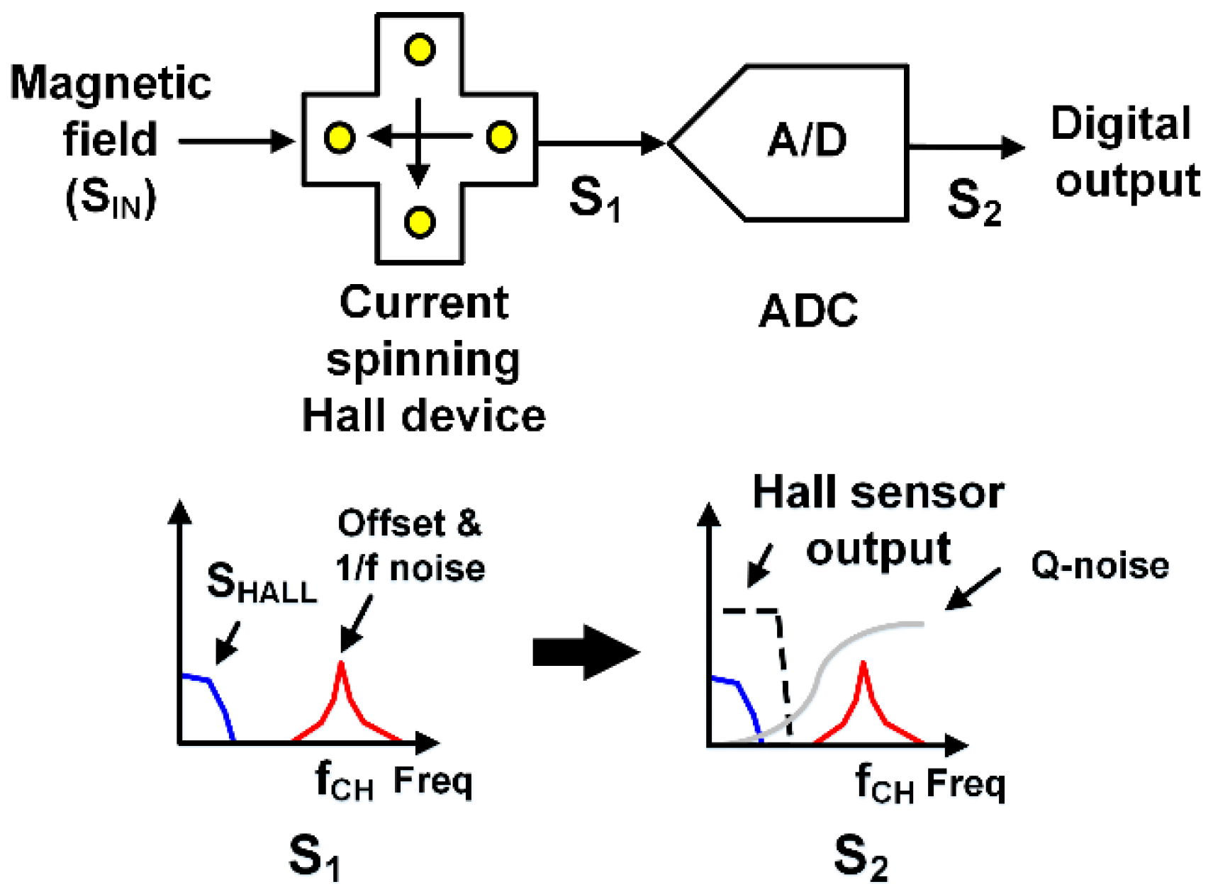
Figure 3.
(a) Horizontal-type Hall device (b) Vertical-type Hall device.

Figure 4.
Modeling of ideal Hall device with wheastone bridge circuit.

Figure 5.
Modeling of practical Hall device and current spinning technique applied to it.

Figure 6.
Direct connection of CMOS Hall device and high-resolution delta-sigma ADC, and operation timing diagram of Hall sensor.
Figure 6.
Direct connection of CMOS Hall device and high-resolution delta-sigma ADC, and operation timing diagram of Hall sensor.

Figure 7.
Hall sensor using double sampling delta-sigma ADC, and its operation timing diagram.

Figure 8.
Cross-sectional Horizontal-type CMOS Hall device layout.

Figure 9.
3rd-order Discrete-time Delta-Sigma ADC block diagram.

Figure 10.
Input referred noise vs. frequency plot of amplifier.

Figure 11.
Adaptive LDO for amplifier supply voltage and replica circuit for reference voltage.

Figure 12.
Inverter based pseudo differential amplifier and switched-capacitor common mode feedback circuit.
Figure 12.
Inverter based pseudo differential amplifier and switched-capacitor common mode feedback circuit.
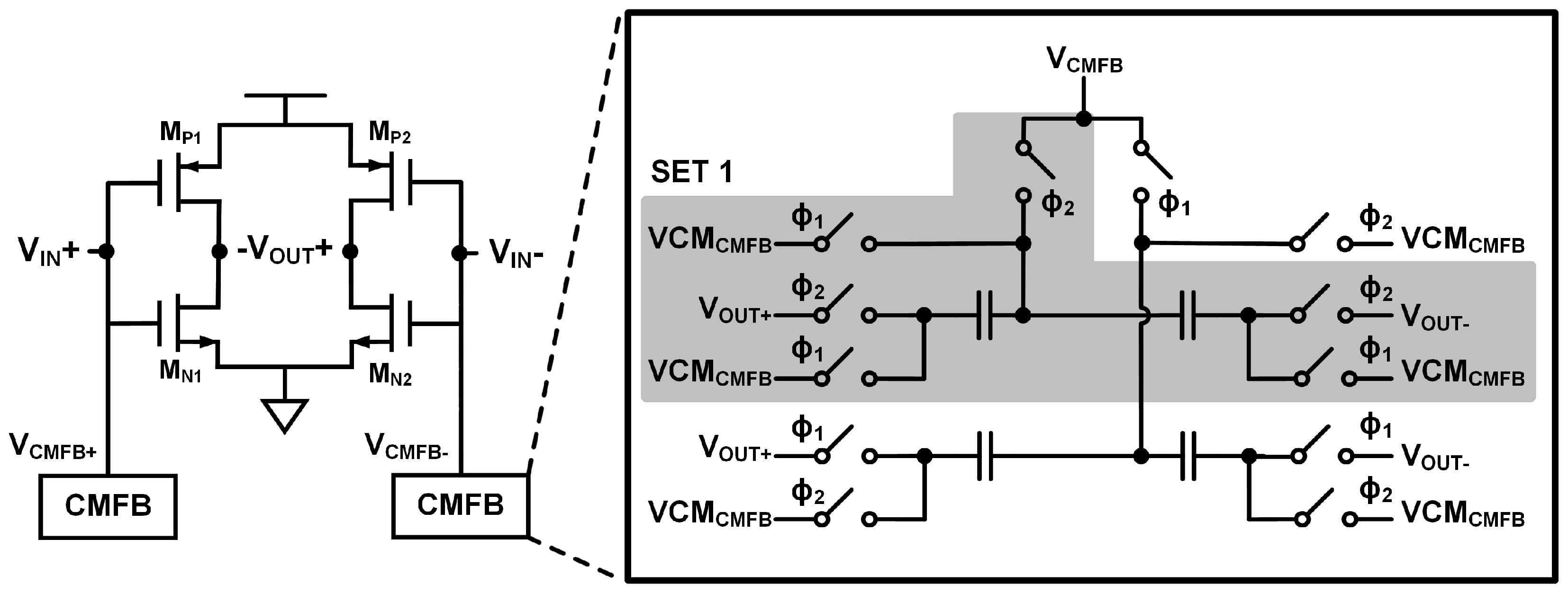
Figure 13.
Multi-input comparator summing three integrator output signals.

Figure 14.
Simulated output power spectral density of standalone delta-sigma ADC.
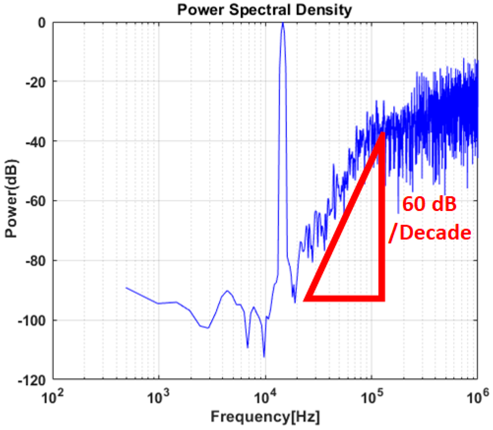
Figure 15.
Die photograph of Hall sensor prototype fabricated in 0.18 µm CMOS process.

Figure 16.
Measured output power spectral density of prototype when DC magnetic field of 150 mT is applied.
Figure 16.
Measured output power spectral density of prototype when DC magnetic field of 150 mT is applied.
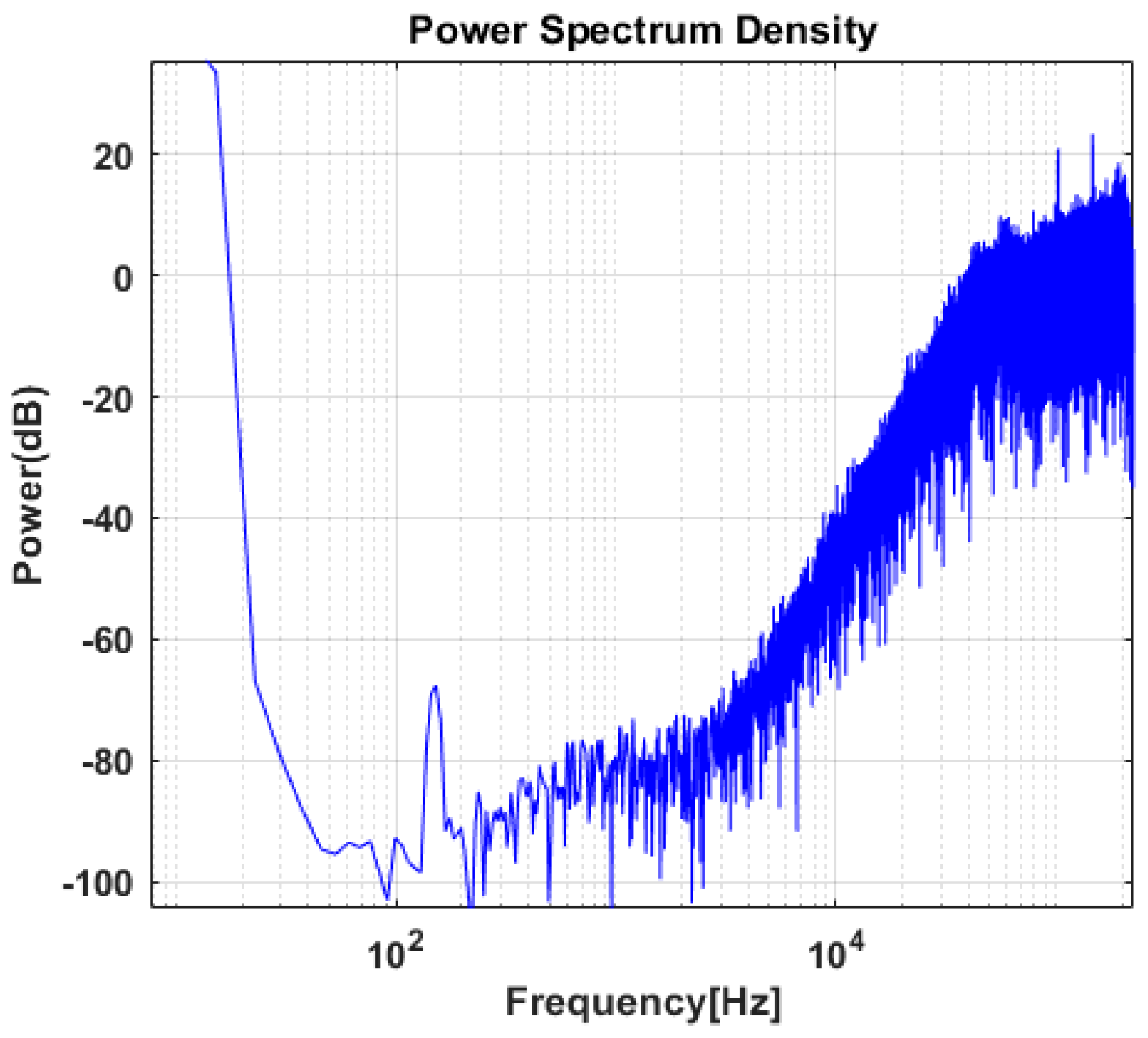
Figure 17.
Normalized Hall output voltage versus input magnetic flux density from measurement of Hall sensor prototype.
Figure 17.
Normalized Hall output voltage versus input magnetic flux density from measurement of Hall sensor prototype.


Table 1.
Performance summary and comparison with other CMOS Hall sensors.
| Parameter | [28] | [29] | This Work |
|---|---|---|---|
| Technology | CMOS 0.5 µm | CMOS 0.8 µm | CMOS 0.18 µm |
| Supply Voltage | 5 V | 5 V | 2.2 V |
| Power Consumption | 21 mW | 20 mW | 4.9 mW |
| Measurement Range | ±10.8 mT | ±175 mT | ±150 mT |
| Offset | 3.65 µT | 0.48 mT | 16 µT |
| Linearity | N/A | >99% | >99% |
| Area | 2.9 mm2 | 1 mm2 | 0.7 mm2 |
© 2020 by the authors. Licensee MDPI, Basel, Switzerland. This article is an open access article distributed under the terms and conditions of the Creative Commons Attribution (CC BY) license (http://creativecommons.org/licenses/by/4.0/).
Share and Cite
MDPI and ACS Style
Lee, J.; Oh, Y.; Oh, S.; Chae, H. Low Power CMOS-Based Hall Sensor with Simple Structure Using Double-Sampling Delta-Sigma ADC. Sensors 2020, 20, 5285. https://doi.org/10.3390/s20185285
AMA Style
Lee J, Oh Y, Oh S, Chae H. Low Power CMOS-Based Hall Sensor with Simple Structure Using Double-Sampling Delta-Sigma ADC. Sensors. 2020; 20(18):5285. https://doi.org/10.3390/s20185285
Chicago/Turabian StyleLee, Juyong, Younggyun Oh, Sein Oh, and Hyungil Chae. 2020. "Low Power CMOS-Based Hall Sensor with Simple Structure Using Double-Sampling Delta-Sigma ADC" Sensors 20, no. 18: 5285. https://doi.org/10.3390/s20185285
Note that from the first issue of 2016, this journal uses article numbers instead of page numbers. See further details here.