Article

PCB Defect Detection via Local Detail and Global Dependency Information

1
Xidian University, Xi’an 710126, China
2
Wide Band Gap Semiconductor Technology State Key Laboratory, Xidian University, Xi’an 710071, China
*
Author to whom correspondence should be addressed.
Sensors 2023, 23(18), 7755; https://doi.org/10.3390/s23187755
Submission received: 13 July 2023 / Revised: 18 August 2023 / Accepted: 28 August 2023 / Published: 8 September 2023
(This article belongs to the Special Issue Deep-Learning-Based Defect Detection for Smart Manufacturing)

Abstract

:
Due to the impact of the production environment, there may be quality issues on the surface of printed circuit boards (PCBs), which could result in significant economic losses during the application process. As a result, PCB surface defect detection has become an essential step for managing PCB production quality. With the continuous advancement of PCB production technology, defects on PCBs now exhibit characteristics such as small areas and diverse styles. Utilizing global information plays a crucial role in detecting these small and variable defects. To address this challenge, we propose a novel defect detection framework named Defect Detection TRansformer (DDTR), which combines convolutional neural networks (CNNs) and transformer architectures. In the backbone, we employ the Residual Swin Transformer (ResSwinT) to extract both local detail information using ResNet and global dependency information through the Swin Transformer. This approach allows us to capture multi-scale features and enhance feature expression capabilities.In the neck of the network, we introduce spatial and channel multi-head self-attention (SCSA), enabling the network to focus on advantageous features in different dimensions. Moving to the head, we employ multiple cascaded detectors and classifiers to further improve defect detection accuracy. We conducted extensive experiments on the PKU-Market-PCB and DeepPCB datasets. Comparing our proposed DDTR framework with existing common methods, we achieved the highest F1-score and produced the most informative visualization results. Lastly, ablation experiments were performed to demonstrate the feasibility of individual modules within the DDTR framework. These experiments confirmed the effectiveness and contributions of our approach.

1. Introduction

With the emergence of Industry 4.0, production processes have been enhanced by incorporating cyber-physical systems that utilize an increased number of circuit boards to create intelligent systems. To ensure the integrity of the circuit board layout, each element needs to be carefully designed, including the through-holes in the hardware, to guarantee high operational reliability. However, due to process uncertainty and noise, ensuring the integrity of all produced circuit boards becomes challenging. Nevertheless, various machine vision-based methods have been introduced to detect defects. With the upgrading of the PCB production process, the circuit density of PCBs is increasing. The defects generated during the PCB production process exhibit characteristics such as small area, large quantity, and different shapes, requiring PCB defect detection methods to be highly precise and fast. The rapid and widespread adoption of deep learning algorithms has led to the development of numerous deep learning-based techniques in the field of electronic circuits, particularly in identifying flaws in printed circuit boards (PCBs). The primary purpose of a PCB is to provide mechanical support for connecting electronic components, achieved through pads, conductive tracks, and soldering. However, environmental factors make PCB surfaces highly vulnerable to quality issues that deviate from design and manufacturing specifications. For instance, Figure 1 displays six types of PCB defects: spur, mouse bite, spurious copper, missing hole, short circuit, and open circuit. These defects not only significantly affect the quality and performance of final products but also result in substantial economic losses for relevant industries. As a result, detecting flaws on PCB surfaces has become a crucial process in managing PCB production quality, attracting significant attention from the industry.
Through the adoption of automated optical inspection (AOI) techniques [1], manual inspections have been largely replaced, leading to enhanced detection accuracy and efficiency. While AOI systems are more convenient and cost-effective than human inspection, they heavily rely on visible imaging sensors, which can be limiting. The quality of PCB images captured by these visible imaging sensors is significantly impacted by illumination conditions, resulting in uneven brightness levels and decreased detection accuracy for various defect types.
Traditional defect detection methods utilize image-processing techniques, prior knowledge, and conventional machine learning approaches to extract low-level features related to defects. However, these methods necessitate the creation of specific classifiers for different defect categories, which restricts their applicability across various application scenarios. In recent years, a range of image processing algorithms have been investigated for PCB defect detection. These include similarity measurement approaches [2], segmentation-based methods [3], and binary morphological image processing [4]. Nevertheless, these techniques require the alignment of inspected images with standard samples during defect inspection. Therefore, there is an urgent need to develop a novel defect detection framework capable of adapting to diverse defect types seamlessly.
The introduction of deep learning has brought significant advancements to object detection, including techniques such as fast R-CNN [5], RetinaNet [6], and You Only Look Once (YOLO) [7], which have demonstrated impressive capabilities in feature extraction. However, when it comes to PCB defect detection, these methods face certain limitations due to the local feature nature of convolutional neural networks (CNN) [8,9]. Defect detection regions on PCBs often occupy only a small portion of the overall image, and even within the same category of surface defects, there can be significant variations in morphology and patterns. While various deep learning-based detectors have been developed to address these challenges, current detectors struggle to simultaneously achieve high detection accuracy, fast detection speed, and low memory consumption. Therefore, there is a need to explore innovative approaches that can effectively address these limitations and meet the requirements of high accuracy, efficient processing, and optimized resource utilization in PCB defect detection.
In recent years, transformer-based deep learning methods have shown remarkable achievements. Within the domain of object detection, transformers [10] have surpassed convolutional neural networks (CNNs) in terms of accuracy. Prominent examples include DETR [11] and Swin Transformer [12]. Unlike CNNs, which are limited to extracting local features within their receptive fields, transformers have the capability to capture global dependency information even in shallow network architectures. This characteristic is especially advantageous for recognition and detection tasks.
However, transformers suffer from the drawback of high computational complexity. To address this issue, a common approach is to divide the input image into patches before feeding them into the transformer. Although this solves the computational challenge, it inevitably results in a loss of local detail information. Therefore, the combination of CNN and transformer has emerged as an optimal solution in numerous tasks across various fields. By utilizing CNN to extract local detail information and transformer to capture global dependency information, superior performance has been demonstrated.
Given the aforementioned problems, we propose a novel PCB surface defeat detection network. To take full advantage of the deep information provided by the source input images, we design a novel two-way cascading feature extractor.
A novel dual cascaded feature extractor, Residual Swin Transformer (ResSwinT), consisting of ResNet and Swin Transformer, is proposed, which can simultaneously focus on local detail information and global dependency information of images. By utilizing the spatial and channel features of spatial multi-head self-attention (SSA) and channel multi-head self-attention (CSA) fusion features, the network can focus on advantageous features. A large number of experiments have been conducted on the PKU Market PCB dataset and DeepPCB dataset, proving that our proposed defect detection converter (DDTR) can better detect difficult defect targets, achieve higher precision defect detection, and improve the yield of PCB production.

2. Related Works

2.1. PCB Defeat Detection

Over the past few decades, numerous vision-based defect detection methods have been introduced in the field of PCB defect detection. For instance, Tang et al. [13] developed a deep model capable of accurately detecting defects by analyzing a pair of input images—an unblemished template and a tested image. They incorporated a novel group pyramid pooling module to efficiently extract features at various resolutions, which were then merged by groups to predict corresponding scale defects on the PCB. Recognizing the complexity and diversity of PCBs, Ding et al. [14] proposed a lightweight defect detection network based on the fast R-CNN framework. This method leveraged the inherent multi-scale and pyramidal hierarchies of deep convolutional networks to construct feature pyramids, strengthening the relationship between feature maps from different levels and providing low-level structural information for detecting tiny defects. Additionally, they employed online hard example mining during training to mitigate the challenges posed by small datasets and data imbalance. Kim et al. [15] developed an advanced PCB inspection system based on a skip-connected convolutional autoencoder. The deep autoencoder model was trained to reconstruct non-defective images from defect images. By comparing the reconstructed images with the input image, the location of the defect could be identified. In recent years, significant progress has been made in object detection, including the rapid development of algorithms such as YOLO. Liao et al. [16] introduced a cost-efficient PCB surface defect detection system based on the state-of-the-art YOLOv4 framework. Free from the constraints of visible imaging sensors, Li et al. [17] designed a multi-source image acquisition system that simultaneously captured brightness intensity, polarization, and infrared intensity. They then developed a Multi-sensor Lightweight Detection Network that fused polarization information and brightness intensities from the visible and thermal infrared spectra for defect detection on PCBs.
Addressing the challenges posed by small defect targets and limited available samples in the application of deep learning methods to real-world enterprise scenarios for PCB defect detection, this paper presents a novel approach. The proposed method involves a dual-way cascading feature extractor to extract more comprehensive and refined features from PCB images. By employing this feature extractor, the model can effectively capture relevant information for defect detection.
Furthermore, the paper introduces a multi-head spatial and channel self-attention fusion algorithm. This algorithm enables the model to leverage the benefits of focusing on different sizes and channel features of PCB defects. By applying spatial and channel self-attention mechanisms, the model can selectively attend to relevant regions and channels, enhancing its ability to detect defects accurately.
These advancements in feature extraction and attention fusion contribute to overcoming the limitations commonly encountered in PCB defect detection. The proposed approach has the potential to improve the performance and robustness of deep learning models when applied to various enterprise scenarios for PCB defect detection.

2.2. Visual Transformer

The Vision Transformer (ViT) architecture, introduced by Google in 2020, has proven to be an effective deep learning approach for a wide range of visual tasks. It serves as a general-purpose backbone for various downstream tasks, including image classification [18], object detection [19], semantic segmentation [20,21], human pose estimation [22], and image fusion [23,24]. Unlike traditional convolutional neural networks (CNNs), ViT eliminates the need for hand-crafted feature extraction and data augmentation, which can be time-consuming. Additionally, ViT can leverage self-supervised learning techniques to train models without labeled data.
In ViT, an image is divided into a grid of patches, and each patch is flattened into a one-dimensional vector. These patch vectors are then processed by a series of Transformer blocks, which operate in parallel and allow the model to attend to different parts of the image. The output of the last Transformer block is fed into a multi-layer perceptron to generate class predictions. ViT has achieved best performance on image classification benchmarks, such as CIFAR, and has outperformed previous methods in multiple computer vision tasks.
Researchers have explored and extended ViT for different applications. For instance, Smriti et al. [25] compared ViT with various CNNs and transformer-based methods for medical image classification tasks, demonstrating that ViT achieved state-of-the-art performance and surpassed CNN and data-efficient Image Transformer-based models. Zhu et al. introduced weakTr [26], a concise and efficient framework based on plain ViT, for weakly supervised semantic segmentation. This approach enabled the generation of high-quality class activation maps and efficient online retraining. Additionally, a saliency-guided vision transformer [27] was proposed for few-shot keypoints detection, incorporating masked self-attention and a morphology learner to constrain attention to foreground regions and adjust the morphology of saliency maps.
In the context of PCB defect detection, the proposed Dual-branch Detection Transformer (DDTR) utilizes a ResSwinT to encode global dependencies and extract comprehensive features. This enables the subsequent detection branch to achieve robust and comprehensive features for defect detection, resulting in notable advancements in detection accuracy for the model.
Overall, ViT has proven to be a versatile and effective architecture in computer vision tasks, and its application and extensions show promising results across various domains, including medical imaging, semantic segmentation, and keypoints detection. In the field of PCB defect detection, the DDTR model leverages the strengths of ViT to improve the accuracy and robustness of the detection process.

3. Methodology

Since the introduction of the Swin Transformer, numerous methods employing this architecture have demonstrated remarkable performance in object detection. Given its unique ability for parallel computing and managing global dependencies, the Swin Transformer is employed to extract more comprehensive object information. Furthermore, traditional CNNs can be employed to uncover edge features through shallow convolutional layers and high-level features through deeper layers. This paper proposes their combination to offer abundant semantic information for subsequent detections. Additionally, we introduce a multi-source self-attention fusion strategy to bolster the robustness and flexibility of our model.

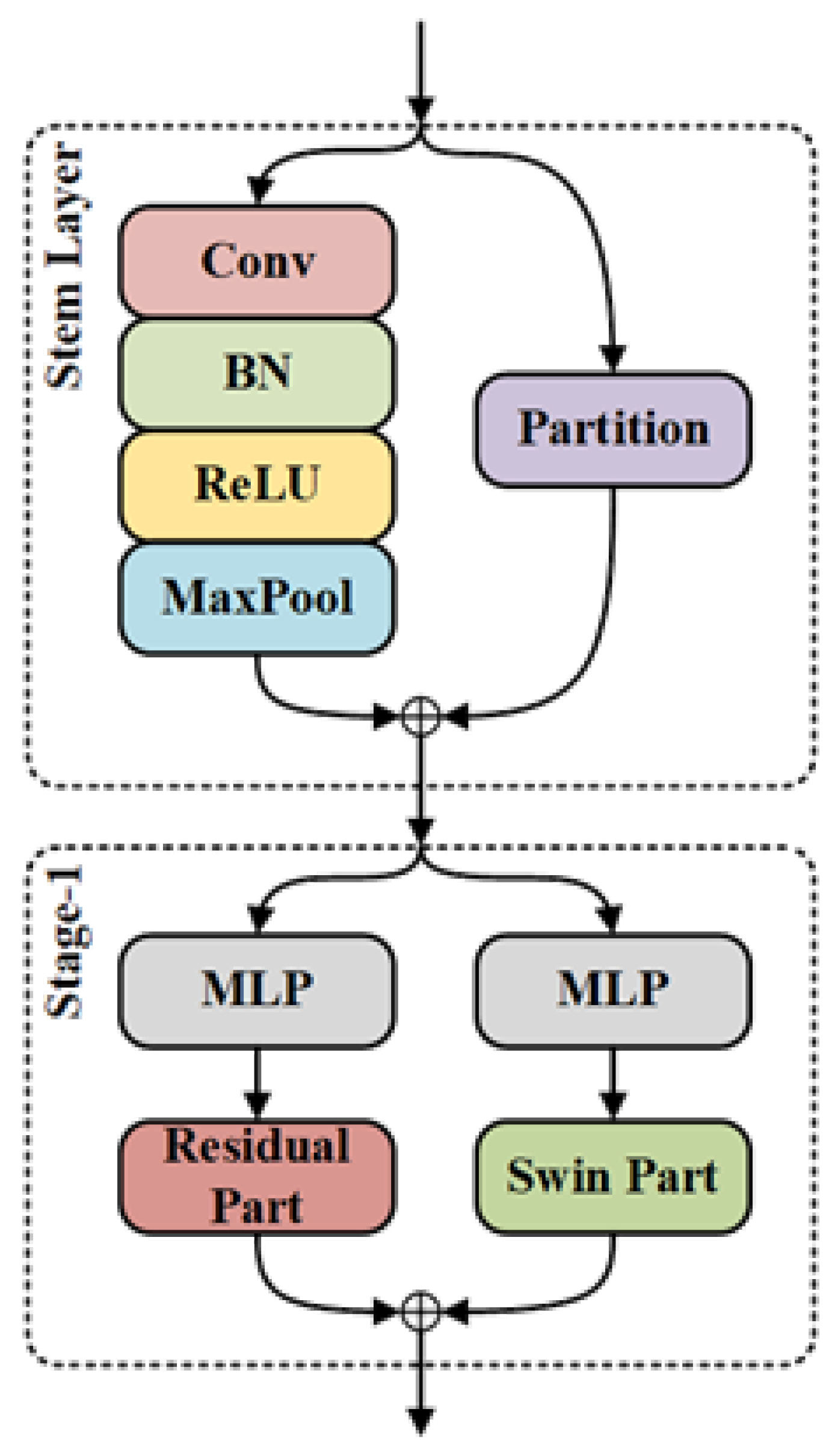
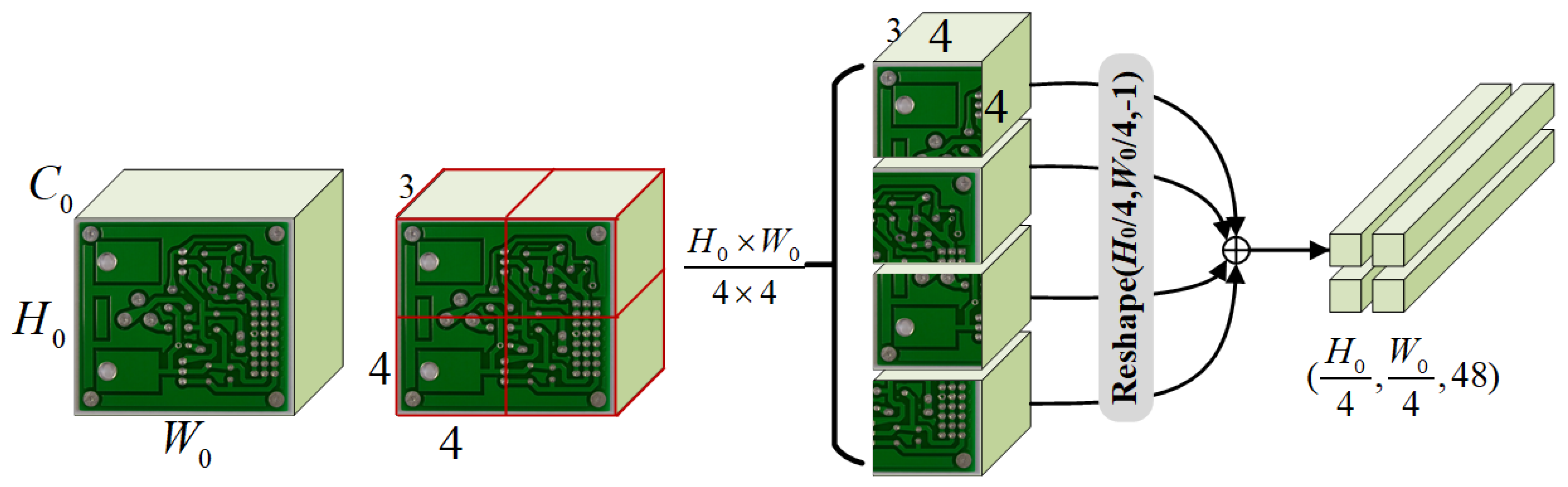
3.1. Overall Architecture

The structure of our proposed DDTR as shown in Figure 2 is similar to the existing object detection network Cascade R-CNN [28]. It can be divided into a backbone for feature extraction, a neck for feature enhancement, and a head for recognition and detection.
Firstly, the image X R H 0 × W 0 × C 0 is input into a dual backbone network called ResSwinT composed of Resnet and Swin Transformer. The multi-scale features obtained by ResSwinT are represented as X i R H i × W i × C i , where i = 1 , 2 , 3 , 4 . In the neck, feature enhancement is performed by mixing convolutional layers and Transformer. Due to the various shapes of defects on PCBs, DDTR introduces a spatial attention mechanism to enable the network to adaptively perceive important spatial features. Furthermore, the features extracted by the backbone exhibit high dimensionality in terms of channels. DDTR will emphasize significant channels through channel attention. Ultimately, the same cascade heads used in Cascade R-CNN are employed to enhance the accuracy of PCB defect recognition and detection in the head of DDTR.

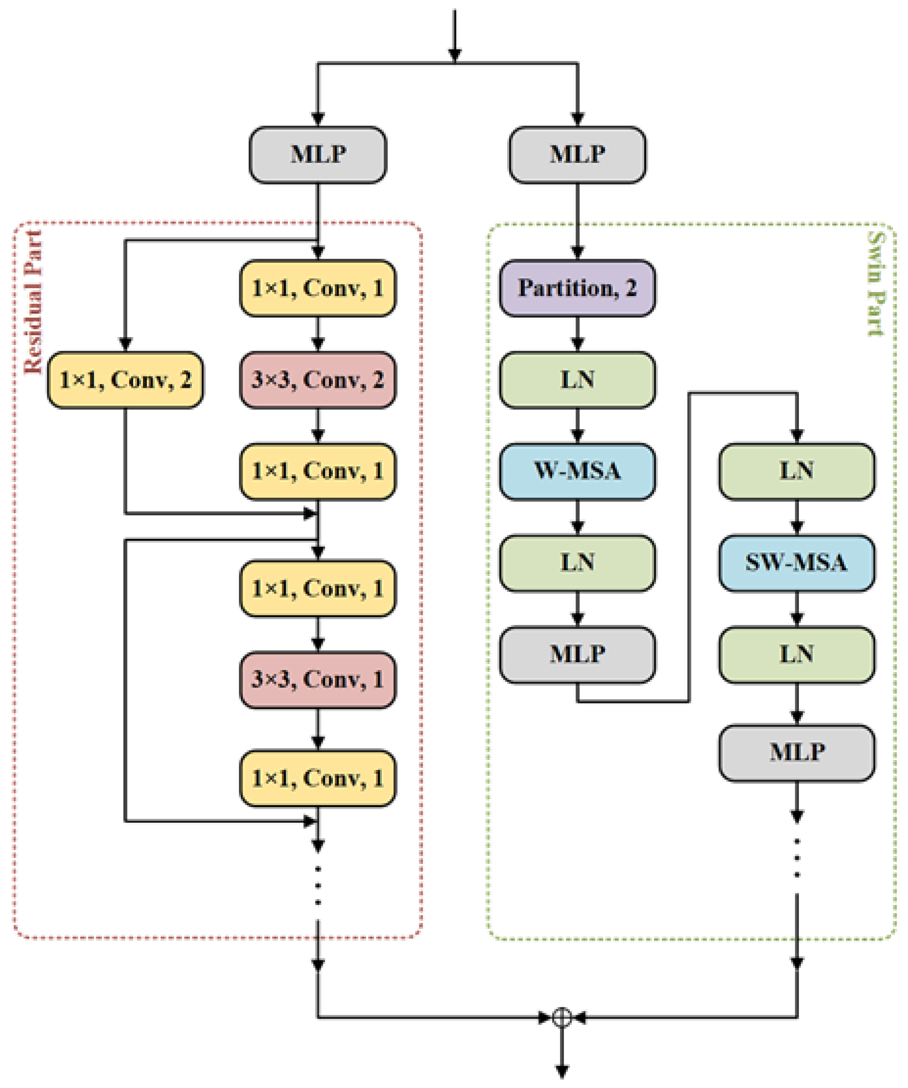
3.2. Residual Swin Transformer (ResSwinT)

While traditional single-path CNNs can offer computational and memory efficiency, their extraction of local features alone restricts the model from capturing the broader contextual information present in the input image. This limitation proves critical for the detection of minute defects in PCBs. To address this, we introduce a dual backbone network called ResSwinT, illustrated in Figure 3. ResSwinT combines the residual modules of ResNet with the self-attention mechanism of Swin Transformer, which employs shift windows, to produce multi-scale features encompassing both global and local information within the feature space.
In the initial stage of ResSwinT, the image X R H 0 × W 0 × C 0 will generate a feature X 0 R H 0 / 4 × W 0 / 4 × 112 through the stem layer containing a partition and a convolutional layer. The input image X in the partition is divided into patches of size 4 × 4 and flattened to obtain X p R H 0 / 4 × W 0 / 4 × 48 . The stem layer contains convolution and max-pooling with a stride of 2, and its output is X c R H 0 / 4 × W 0 / 4 × 64 . So the calculation process is
X p = P a r t i t i o n ( X )
X c = M a x p o o l ( C o n v ( X ) )
X 0 = X p X c
where ⊕ represents the channel concatenation.
The subsequent structure of ResSwinT consists of four stages, each consisting of multi-layers perceptron (MLP), a residual part, and a swin part. In order to load the pre-trained weights from ResNet and Swin Transformer, we do not change the structure of the residual and swin parts. The input feature X i 1 in i-th stage is first adjusted through MLP to match the channel in the pre-trained network. The residual part of i-th stage contains n i r residual layers, which are composed of convolution, batch normalization (BN) [29], ReLU [30] and shortcut, as shown in Figure 4. Its calculation process is
f r ( X ) = R e s ( X ) + X ,
where R e s ( · ) represents three convolution layers in the residual layer. By using the shortcut of the residual layer, the degradation problem of deep networks can be solved.
Due to partition in the stem layer, only MLP is used to adjust the channel in stage 1. However, in stage 2, 3, and 4, down-sampling is performed through partition before feature extraction by swin transformer blocks. The swin transformer blocks contain two transformer encoders, which are composed of multi-head self-attention (MSA), feed forward (FF) network, and layer normalization (LN) [31], as shown in Figure 4. Unlike the MSA of the transformer, the swin transformer adopts window multi-head self-attention (W-MSA). In the W-MSA of the first encoder, the feature X only calculates local dependency information within the window of (w, w), as shown in Figure 4. In the next encoder, the window is shifted by ( w / 2 , w / 2 ) to expand the area of extracting dependency information, as shown in Figure 4. Its calculation process is
Z i t = W M S A ( L N ( X i t ) ) + X i t
X ^ i t = F F ( L N ( Z i t ) ) + Z i t
Z ^ i t = S W M S A ( L N ( X ^ i t ) ) + X ^ i t
X i t = F F ( L N ( Z ^ i t ) ) + Z ^ i t
Through n i s swin transformer blocks in the i-th stage, global dependency information can be gradually extracted with less computational cost.
In summary, the calculation of ResSwinT is
X i r = f i r ( W i X i 1 )
X i s = f i s ( W i X i 1 )
X i = X i r X i s
where W i is the weight of MLP in i-th stage, X i r R H i × W i × C i r is the multi-scale features obtained by the residual part f i r ( · ) , X i s H i × W i × C i s is the multi-scale features extracted by the swin part f i s ( · ) , where:
H i = H 0 / ( 4 × 2 ( i 1 ) )
W i = W 0 / ( 4 × 2 ( i 1 ) )
C i r = C 1 r × 2 ( i 1 )
C i s = C 1 s × 2 ( i 1 )
where i = 1,2,3,4. Then, X i R H i × W i × C i generated by the channel concatenation between X i r and X i s is fed into the next stage, where:
C i = C i r + C i s

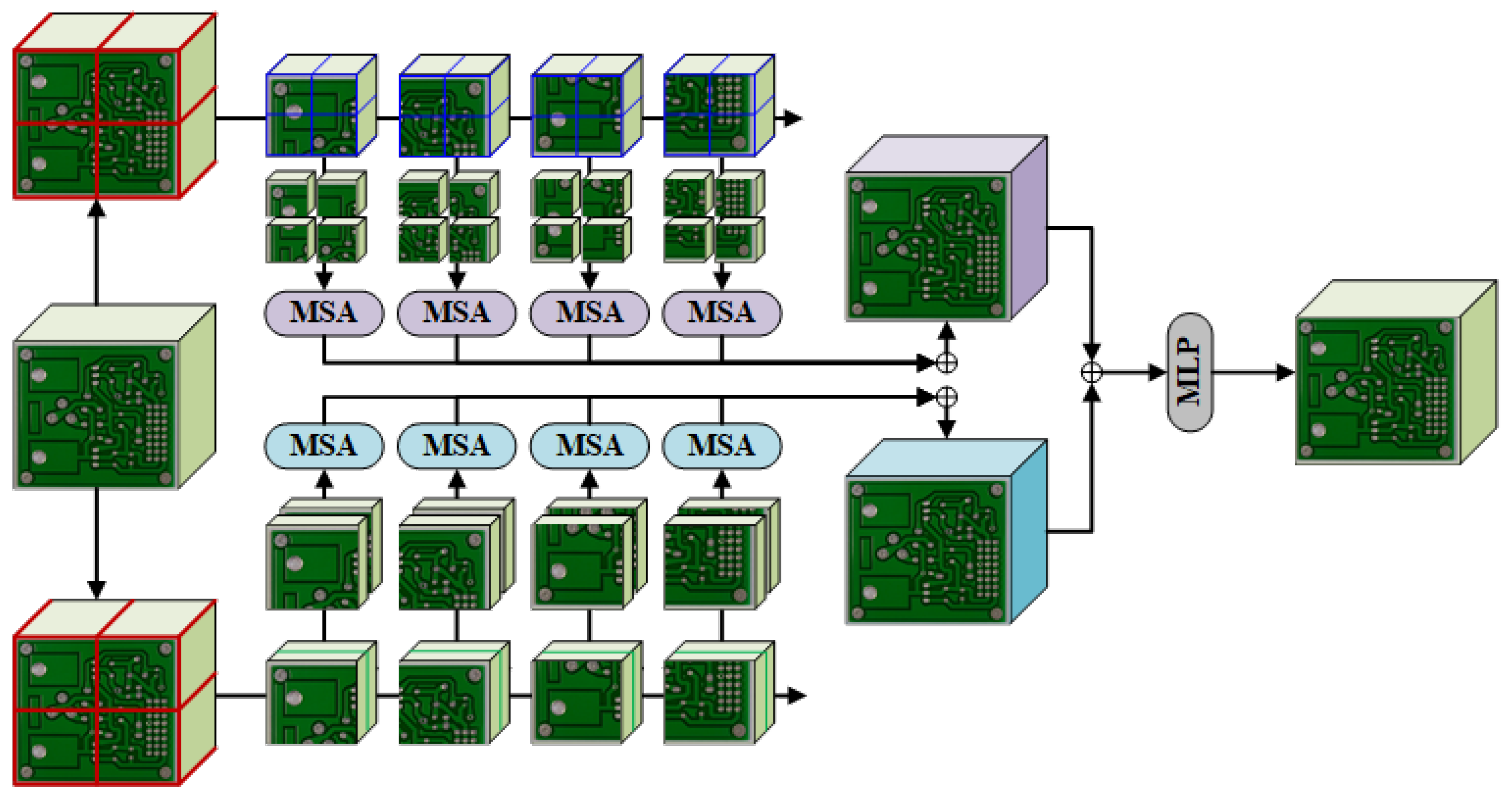
3.3. Multi-Head Spatial and Channel Self-Attention

In the object detection network, the Neck connects the backbone and head, completing the task of feature enhancement. In recent years, multi-scales feature fusion networks have shown significant improvements in accuracy, such as feature pyramid networks (FPN) [32]. We propose a new multi-scale feature fusion strategy named multi-head spatial and channel self-attention (SCSA), as shown in Figure 5. SCSA includes spatial self-attention (SSA) and channel self-attention (CSA), aiming to solve the problem of difficulty in correctly identifying defect targets due to significant differences in PCB defect size, shape, and channel information.

3.3.1. SSA

Due to the large amount of computation involved in the global spatial attention, X i is firstly partitioned according to the size of a × a to obtain A i R M i A × a 2 × C i , as shown in Figure 6, where M i A = H i × W i / a 2 . Afterwards, the A i in each region will be clipped into P i R M i A × M i P × ( a 2 × C i ) in units of p × p as shown in Figure 5 and the embedded feature P ^ i R M i A × M i P × d will be obtained by MLP, where M i P = a 2 / p 2 . By using an encoder of SSA to extract dependency information within local regions, its structure is shown in Figure 5, and its calculation process can be represented as
P ^ i = W i P i
F ^ i s = M S A ( L N ( P ^ i ) ) + P ^ i
F i s = F F ( L N ( F ^ i s ) ) + F ^ i s
where W i is the embedded weight. The MSA is the same as the MSA in the original transformer. Query vectors Q R M i A × M i P × d key vectors K R M i A × M i P × d , and value vectors V R M i A × M i P × d are generated by
[ Q i , K i , V i ] = [ W i Q P ^ i , W i K P ^ i , W i V P ^ i ] ,
where W i Q , W i K , and W i V are the weights of the linear layer. Use key vectors to query on the query vectors, and the query results are the sum weights corresponding to the value vectors. The attention calculation process in MSA is as follows:
M S A ( X ) = A t t e n t i o n ( Q , K , V ) = s o f t m a x ( Q K T d ) V ,
where d is the dimension of the vectors. In the calculation process of MSA, all vectors are evenly divided into each head for self-attention.

3.3.2. CSA

The features of the backbone are obtained by concatenating the features of two branches on channel, resulting in a large amount of redundancy in the features. CSA can calculate channel self-attention through spatial embedding encoding, making the network more focused on advantageous channel features.
Similarly, CSA will first partition X i to obtain A i , but will not further clip the feature into patches. Secondly, the transformed feature A i R M i A × C i × a 2 is used to calculate channel self-attention. By using an encoder of CSA to extract dependency information within local regions, its structure is shown in Figure 5, and its calculation process can be represented as
A ^ i = W i A i T
F ^ i c = M S A ( L N ( A ^ i ) ) + A ^ i
F i c = F F ( L N ( F ^ i c ) ) + F ^ i c
where W i is the embedded weight. In SSA, patches are embedded in the channel dimension, and spatial self-attention is the weighted sum between all patches. However, CSA is embedded features within the channel, and channel self-attention is the weighted sum between channels.

4. Experiment Results

4.1. Datasets

In this section, the PKU-Market-PCB [33] dataset and DeepPCB [13] dataset are used to validate the performance of our proposed DDTR model.

4.1.1. PKU-Market-PCB Dataset

There are 693 PCB defect images in the PKU-Market-PCB dataset, with an average shape of 2240 × 2016 . PCB defects include six types: missing hole, short, mouse bite, spur, open circuits, and Spurious copper. The image only contains one defect type, but there may be multiple defect targets. The training set contains a total of 541 images, the test set contains 152 images.
Because of the large size of the image, the hardware cannot directly train and test on the initial images. Therefore, we cropped all images into 512 × 512 patches. Finally, the training dataset contained 8508 images, while the test set contained 2897 images. More detailed information can be found in Table 1.

4.1.2. DeepPCB Dataset

All images in the DeepPCB dataset were obtained from linear scanning CCD, with a resolution of approximately 48 pixels per 1 millimeter. Then, they are cropped into many sub images of size 640 × 640 and aligned using template matching technology. In order to avoid illumination interference, images are converted to binary image after carefully selecting the threshold. The dataset is manually annotated with six common PCB defect types: open, short, mouse bite, spur, copper, and pin hole. The training set contains a total of 1000 images, the test set contains 500 images, and some instance images are shown in Figure 7. In addition, the number of targets in the dataset is shown in Table 2.

4.2. Evaluation Metrics

First, the confusion matrix between the ground truth and the prediction results of the test set is calculated. When the predicted category is the same as the ground truth category, and the Intersection over Union (IoU) between the predicted box and the ground truth box is not lower than the threshold, the prediction is considered correct. True positive (TP) is the number of positive samples for both the ground truth and the predicted result. False positive (FP) is defined as the number of samples with negative ground truth and positive predicted results. True negative (TN) is the number of negative samples for both ground truth and predicted results. False negative (FN) is defined as the number of samples with positive ground truth and negative predicted results.
We used F1-score, which is commonly used in the field of object detection, as the metric for verifying performance. The definition of F1-score is as follows
F 1 s c o r e = 2 × P × R P + R
where P is the precision, defined as
P = T P T P + F P .
R is the recall, and the calculation formula is
R = T P T P + F N .

4.3. Implemental Details

We have designed two types of ResSwinT for DDTR. One is the ResSwinT-T based on ResNet50 and SwinT-T, which has a slightly smaller computational complexity. The another is ResSwinT-S based on ResNet101 and SwinT-S, which has a slightly higher computational complexity. The information for the two types of ResSwinT is shown in Table 3. For SSA in SCSA, the area is 4 × 4 , the patch is 1 × 1 , and the input feature dimension for each head is 32. For CSA in SCSA, the area is 10 × 10 , and the input feature dimension for each head is 25.
To verify the effectiveness of our proposed DDTR, we compared it with six advanced object detection methods, including: (1) one-stage methods: YOLOv3, SSD [34], ID-YOLO [35] and LightNet [36]; (2) two-stage methods: faster R-CNN [37] and cascade R-CNN. During the training and testing process, all methods use a fixed input size of 640 × 640 . All the methods are trained on a Ubuntu18.04 server equipped with E5 2697v3 and RTX3090. Python is 3.7, PyTorch is 1.13.1, and CUDA is 11.7.

4.4. Experimental Results

4.4.1. Experimental Results of PKU-Market-PCB

The precision results on the PKU-Market-PCB dataset are shown in Table 4. From the results, it can be seen that the accuracy of all two-stage methods exceeds one-stage object detection methods. A backbone based on the Transformer architecture has higher detection and recognition accuracy compared to CNN. The proposed DDTR method achieved the best results in AP, AR, and F1-scores. Compared to YOLOv3, the DDTR improved 15.42% on F1-score.
From the visualization results in Figure 8, the SSD and YOLO of one-stage object detection have more false alarms. Due to the lack of global dependency information, there are some overlapping target results in CNN-based object detection methods, which are alleviated after using transformer. The proposed DDTR method has good visualization results on the PKU-Market-PCB dataset.

4.4.2. Experimental Results of DeepPCB

The accuracy results of the DeepPCB dataset are shown in Table 5. From the results, it can be seen that the accuracy of all two-stage methods equally exceeds that of the one-stage target detection methods. Compared to CNN, the Transformer-based backbone has higher detection and recognition accuracy. The proposed DDTR method achieved the best results in AP, AR, and F1-score. Compared to YOLOv3, the DDTR has improved 9.04% on F1-score.
From the visualization results in Figure 9, it can be seen that SSD and YOLO have more false alarms. Due to the lack of global dependency information, there are some overlapping target results in CNN-based object detection methods, which have been alleviated by the use of transformer. Due to the lack of attention information, all comparison methods have a significant amount of false positives in the digital area. The proposed DDTR method has good visualization performance on the DeepPCB dataset.

4.5. Ablation Experiments

We conducted some ablation experiments on the proposed module, as shown in Table 6, where the best performing ones are highlighted in bold. Firstly, we use ResNet101 Cascade R-CNN as the baseline, which has 0.3813 F1-score on the PKU-MARKET-PCB dataset. If SwinT-S is used to replace ResNet101, it has a 0.89% improvement. If the proposed ResSwinT-S is used as the backbone, it has a 2.89% improvement. On this basis, networks using SSA have a 4.44% improvement compared to Baseline, and networks using CSA is 4.69%. The difference between the SSA and CSA is not significant, indicating that SSA and CSA can enhance the expression ability of features in different dimensions. When ResSwinT-S and SCSA are introduced simultaneously, addition of the feature SSA and CSA shows a 5.99% improvement, while channel concatenation is 6.19%.

5. Conclusions

DDTR has designed a new backbone for extracting multi-scale features, named ResSwinT. ResSwinT combines ResNet and Swin Transformer to extract local details and global dependency information. And it can load pre-trained model weights to assist training. Secondly, due to the higher complexity of the features extracted by ResSwinT, we designed a spatial channel multi-head self-attention structure. Spatial multi-head self-attention can encode space features through channel information, and use a self-attention mechanism to achieve weighted summation of spatial features within the region. Channel multi-head self-attention can encode channel features through spatial information, and use a self-attention mechanism to achieve a weighted sum of channel features within the region.
We conducted extensive experiments on the PKU-MARKET-PCB and DeepPCB datasets, and compared to the existing one-stage and two-stage detection models, the proposed DDTR can improve the F1-score by up to 15.42%. The results of multiple visualizations also show that DDTR demonstrates better detection performance. To verify the effectiveness of the module, we conducted a series of ablation experiments. The results of ablation experiments show that ResSwinT and SCSA can improve the accuracy of defect detection.So if DDTR is applied to automated defect detection in the PCB production process, it can accurately detect PCB defects and improve the yield of PCB production.

Author Contributions

All of the authors made significant contributions to the article. B.F. took on most of the content; J.C. mainly undertook English submission and other tasks. All authors have read and agreed to the published version of the manuscript.

Funding

National Natural Science Foundation of China: 62274123.

Institutional Review Board Statement

Not applicable.

Informed Consent Statement

Not applicable.

Data Availability Statement

The DeepPCB dataset used in this article is available from https://github.com/tangsanli5201/DeepPCB (accessed on 1 July 2023). The PKU-Market-PCB dataset used in this article is available from https://robotics.pkusz.edu.cn/resources/dataset/ (accessed on 1 July 2023).

Conflicts of Interest

The authors declare no conflict of interest.

References

  1. Chen, S.-H.; Perng, D.-B. Automatic optical inspection system for IC molding surface. J. Intell. Manuf. 2016, 27, 915–926. [Google Scholar] [CrossRef]
  2. Gaidhane, V.H.; Hote, Y.V.; Singh, V. An efficient similarity measure approach for pcb surface defect detection. Pattern Anal. Appl. 2017, 21, 277–289. [Google Scholar] [CrossRef]
  3. Kaur, B.; Kaur, G.; Kaur, A. Detection and classification of printed circuit board defects using image subtraction method. In Proceedings of the Recent Advances in Engineering and Computational Sciences (RAECS), Chandigarh, India, 6–8 March 2014; pp. 1–5. [Google Scholar]
  4. Malge, P.S.; Nadaf, R.S. PCB defect detection, classification and localization using mathematical morphology and image processing tools. Int. J. Comput. Appl. 2014, 87, 40–45. [Google Scholar]
  5. Girshick, B.R. Fast R-CNN. arXiv 2015, arXiv:1504.08083. [Google Scholar]
  6. Lin, T.Y.; Goyal, P.; Girshick, R.; He, K.; Dollár, P. Focal Loss for Dense Object Detection. IEEE Trans. Pattern Anal. Mach. Intell. 2020, 42, 2980–2988. [Google Scholar] [CrossRef]
  7. Redmon, J.; Divvala, S.; Girshick, R.; Farhadi, A. You Only Look Once: Unified, Real-Time Object Detection. arXiv 2015, arXiv:1506.02640. [Google Scholar]
  8. Lecun, Y.; Bottou, L.; Bengio, Y.; Haffner, P. Gradient-based learning applied to document recognition. Proc. IEEE 1998, 86, 2278–2324. [Google Scholar] [CrossRef]
  9. He, K.; Zhang, X.; Ren, S.; Sun, J. Deep Residual Learning for Image Recognition. In Proceedings of the IEEE Conference on Computer Vision and Pattern Recognition, Las Vegas, NV, USA, 27–30 June 2016. [Google Scholar]
  10. Vaswani, A.; Shazeer, N.; Parmar, N.; Uszkoreit, J.; Jones, L.; Gomez, A.N.; Kaiser, Ł.; Polosukhin, I. Attention is all you need. In Proceedings of the Advances in Neural Information Processing Systems 30 (NIPS 2017), Long Beach, CA, USA, 4–9 December 2017. [Google Scholar]
  11. Carion, N.; Massa, F.; Synnaeve, G.; Usunier, N.; Kirillov, A.; Zagoruyko, S. End-to-End Object Detection with Transformers. In European Conference on Computer Vision; Springer International Publishing: Cham, Switzerland, 2020. [Google Scholar]
  12. Liu, Z.; Lin, Y.; Cao, Y.; Hu, H.; Wei, Y.; Zhang, Z.; Lin, S.; Guo, B. Swin Transformer: Hierarchical Vision Transformer using Shifted Windows. In Proceedings of the IEEE/CVF International Conference on Computer Vision, Virtual Conference, 11–17 October 2021. [Google Scholar]
  13. Tang, S.; He, F.; Huang, X.; Yang, J. Online PCB Defect Detector On A New PCB Defect Dataset. arXiv 2019, arXiv:1902.06197. [Google Scholar]
  14. Ding, R.; Dai, L.; Li, G.; Liu, H. TDD-net: A tiny defect detection network for printed circuit boards. CAAI Trans. Intell. Technol. 2019, 4, 110–116. [Google Scholar] [CrossRef]
  15. Kim, J.; Ko, J.; Choi, H.; Kim, H. Printed Circuit Board Defect Detection Using Deep Learning via A Skip-Connected Convolutional Autoencoder. Sensors 2021, 21, 4968. [Google Scholar] [CrossRef]
  16. Liao, X.; Lv, S.; Li, D.; Luo, Y.; Zhu, Z.; Jiang, C. YOLOv4-MN3 for PCB Surface Defect Detection. Appl. Sci. 2021, 11, 11701. [Google Scholar] [CrossRef]
  17. Li, M.; Yao, N.; Liu, S.; Li, S.; Zhao, Y.; Kong, S.G. Multisensor Image Fusion for Automated Detection of Defects”, in Printed Circuit Boards. IEEE Sensors J. 2021, 21, 23390–23399. [Google Scholar] [CrossRef]
  18. Ahmed, I.; Muhammad, S. BTS-ST: Swin transformer network for segmentation and classification of multimodality breast cancer images. Knowl.-Based Syst. 2023, 267, 110393. [Google Scholar]
  19. Wang, Z.; Zhang, W.; Zhang, M.L. Transformer-based Multi-Instance Learning for Weakly Supervised Object Detection. arXiv 2023, arXiv:2303.14999. [Google Scholar]
  20. Lin, F.; Ma, Y.; Tian, S.W. Exploring vision transformer layer choosing for semantic segmentation. In Proceedings of the ICASSP 2023-2023 IEEE International Conference on Acoustics, Speech and Signal Processing (ICASSP), Rhodes Island, Greece, 4–9 June 2023; pp. 1–5. [Google Scholar]
  21. Ru, L.; Zheng, H.; Zhan, Y.; Du, B. Token Contrast for Weakly-Supervised Semantic Segmentation. arXiv 2023, arXiv:2303.01267. [Google Scholar]
  22. Xu, Y.; Zhang, J.; Zhang, Q.; Tao, D. ViTPose+: Vision Transformer Foundation Model for Generic Body Pose Estimation. arXiv 2022, arXiv:2212.04246. [Google Scholar]
  23. Chang, Z.; Feng, Z.; Yang, S.; Gao, Q. AFT: Adaptive Fusion Transformer for Visible and Infrared Images. IEEE Trans. Image Process. 2023, 32, 2077–2092. [Google Scholar] [CrossRef]
  24. Chang, Z.; Yang, S.; Feng, Z.; Gao, Q.; Wang, S.; Cui, Y. Semantic-Relation Transformer for Visible and Infrared Fused Image Quality Assessment. Inf. Fusion 2023, 95, 454–470. [Google Scholar] [CrossRef]
  25. Regmi, S.; Subedi, A.; Bagci, U.; Jha, D. Vision Transformer for Efficient Chest X-ray and Gastrointestinal Image Classification. arXiv 2023, arXiv:2304.11529. [Google Scholar]
  26. Zhu, L.; Li, Y.; Fang, J.; Liu, Y.; Xin, H.; Liu, W.; Wang, X. WeakTr: Exploring Plain Vision Transformer for Weakly-supervised Semantic Segmentation. arXiv 2023, arXiv:2304.01184. [Google Scholar]
  27. Lu, C.; Zhu, H.; Koniusz, P. From Saliency to DINO: Saliency-guided Vision Transformer for Few-shot Keypoint Detection. arXiv 2023, arXiv:2304.03140. [Google Scholar]
  28. Cai, Z.; Vasconcelos, N. Cascade R-CNN: Delving into High Quality Object Detection. In Proceedings of the IEEE Conference on Computer Vision and Pattern Recognition, Honolulu, HI, USA, 21–26 July 2017. [Google Scholar]
  29. Ioffe, S.; Szegedy, C. Batch Normalization: Accelerating Deep Network Training by Reducing Internal Covariate Shift. In Proceedings of the 32nd International Conference on Machine Learning, Lille, France, 6–11 July 2015. [Google Scholar]
  30. Glorot, X.; Bordes, A.; Bengio, Y. Deep Sparse Rectifier Neural Networks. J. Mach. Learn. Res. 2011, 15, 315–323. [Google Scholar]
  31. Ba, J.L.; Kiros, J.R.; Hinton, G.E. Layer Normalization. arXiv 2016, arXiv:1607.06450. [Google Scholar]
  32. Lin, T.Y.; Dollár, P.; Girshick, R.; He, K.; Hariharan, B.; Belongie, S. Feature Pyramid Networks for Object Detection. In Proceedings of the IEEE Conference on Computer Vision and Pattern Recognition, Honolulu, HI, USA, 21–26 July 2017. [Google Scholar]
  33. Huang, W.; Wei, P. A PCB Dataset for Defects Detection and Classification. arXiv 2019, arXiv:1901.08204. [Google Scholar]
  34. Liu, W.; Anguelov, D.; Erhan, D.; Szegedy, C.; Reed, S.; Fu, C.Y.; Berg, A.C. SSD: Single Shot MultiBox Detector. In Computer Vision—ECCV 2016; Leibe, B., Matas, J., Sebe, N., Welling, M., Eds.; Lecture Notes in Computer, Science; Springer: Cham, Switzerland, 2016; Volume 9905, pp. 21–37. [Google Scholar] [CrossRef]
  35. Hao, K.; Chen, G.; Zhao, L.; Li, Z.; Liu, Y. An insulator defect detection model in aerial images based on multiscale feature pyramid network. IEEE Trans. Instrum. Meas. 2022, 71, 1–12. [Google Scholar] [CrossRef]
  36. Liu, J.; Li, H.; Zuo, F.; Zhao, Z.; Lu, S. KD-LightNet: A Lightweight Network Based on Knowledge Distillation for Industrial Defect Detection. IEEE Trans. Instrum. Meas. 2023, 72, 3525713. [Google Scholar] [CrossRef]
  37. Ren, S.; He, K.; Girshick, R.; Sun, J. Faster R-CNN: Towards Real-Time Object Detection with Region Proposal Networks. IEEE Trans. Pattern Anal. Mach. Intell. 2017, 39, 1137–1149. [Google Scholar] [CrossRef]
Figure 1. Some defect examples. (a) Missing hole, (b) Short, (c) Mouse bite, (d) Spur, (e) Open circuit, (f) Spurious copper.
Sensors 23 07755 g001
Figure 2. The overall architecture of DDTR. Firstly, the image is input into a dual backbone network called ResSwinT composed of Resnet and Swin Transformer to obtain the multi-scale features. In the neck, feature enhancement is performed by mixing convolutional layers and Transformer. Due to the various shapes of defects on PCBs, DDTR introduces a spatial attention mechanism to enable the network to adaptively perceive important spatial features. Additionally, the features extracted by the backbone exhibit high dimensionality in terms of channels, and DDTR will prioritize crucial channels through channel attention. Lastly, in the head of DDTR, the same cascade heads as those in Cascade R-CNN are employed to enhance the accuracy of PCB defect recognition and detection.
Sensors 23 07755 g002
Figure 3. The structure of stem layer and stage-1 in ResSwinT.
Sensors 23 07755 g003
Figure 4. The structure of stage-i in ResSwinT.
Sensors 23 07755 g004
Figure 5. The structure of SCSA. The purple background module is SSA, and the blue background module is CSA.
Sensors 23 07755 g005
Figure 6. The operation process of partition.
Sensors 23 07755 g006
Figure 7. Examples of PKU-Market-PCB datasets and DeepPCB datasets.
Sensors 23 07755 g007
Figure 8. Some visualization results on the PKU-Market-PCB dataset. (a) Input image, (b) ground truth, (c) YOLOv3, (d) SSD, (e) Faster R-CNN_ResNet50, (f) Faster R-CNN_ResNet101, (g) Cascade R-CNN_ResNet50, (h) Cascade R-CNN_ResNet101, (i) Cascade R-CNN_SwinT-T, (j) Cascade R-CNN_SwinT-S, (k) DDTR_ResSwinT-T, (l) DDTR_ResSwinT-S.
Sensors 23 07755 g008
Figure 9. Some visualization results on the DeepPCB dataset. (a) Input image, (b) ground truth, (c) YOLOv3, (d) SSD, (e) Faster R-CNN_ResNet50, (f) Faster R-CNN_ResNet101, (g) Cascade R-CNN_ResNet50, (h) Cascade R-CNN_ResNet101, (i) Cascade R-CNN_SwinT-T, (j) Cascade R-CNN_SwinT-S, (k) DDTR_ResSwinT-T, (l) DDTR_ResSwinT-S.
Sensors 23 07755 g009
Table 1. The target number of the PKU-Market-PCB dataset.
Before CroppingAfter Cropping
TrainTestTrainTest
Missing hole3621261637608
Short3511311478551
Mouse bite3651261661547
Spur3701271641587
Open circuits3661261655587
Spurious copper3711321719561
Table 2. The target number of the DeepPCB dataset.
TrainTest
Open1283659
Short1028478
Mouse bite1379586
Spur1142483
Copper1010464
Pin hole1031470
Table 3. The parameters of ResSwinT.
Layer NameOutput SizeResSwinT-TResSwinT-S
Residual PartSwin PartResidual PartSwin Part
Stem layer160 × 160Conv, 64, 7 × 7, stride 2
Maxpool, 3 × 3, stride 2
Partition, 4 × 4Conv, 64, 7 × 7, stride 2
Maxpool, 3 × 3, stride 2
Partition, 4 × 4
Concatenation, 112Concatenation, 112
Stage 1160 × 160MLP, 112, 64
C o n v , 64 , 1 × 1 , 1 C o n v , 64 , 3 × 3 , 1 C o n v , 256 , 1 × 1 , 1 × 3
MLP, 112, 48
MLP, 48, 96
M S A , 96 , 7 × 7 , 3 × 2
MLP, 112, 64
C o n v , 64 , 1 × 1 , 1 C o n v , 64 , 3 × 3 , 1 C o n v , 256 , 1 × 1 , 1 × 3
MLP, 112, 48
MLP, 48, 96
M S A , 96 , 7 × 7 , 3 × 2
Concatenation, 352Concatenation, 352
Stage 280 × 80MLP, 352, 256
C o n v , 128 , 1 × 1 C o n v , 128 , 3 × 3 C o n v , 512 , 1 × 1 × 4
MLP, 352, 96
Partition, 2×2
MLP, 384, 192
M S A , 192 , 7 × 7 , 6 × 2
MLP, 352, 256
C o n v , 128 , 1 × 1 C o n v , 128 , 3 × 3 C o n v , 512 , 1 × 1 × 4
MLP, 352, 96
Partition, 2 × 2
MLP, 384, 192
M S A , 192 , 7 × 7 , 6 × 2
Concatenation, 704Concatenation, 704
Stage 340 × 40MLP, 704, 512
C o n v , 256 , 1 × 1 C o n v , 256 , 3 × 3 C o n v , 1024 , 1 × 1 × 6
MLP, 704, 192
Partition, 2 × 2
MLP, 768, 384
M S A , 384 , 7 × 7 , 12 × 6
MLP, 704, 512
C o n v , 256 , 1 × 1 C o n v , 256 , 3 × 3 C o n v , 1024 , 1 × 1 × 23
MLP, 352, 96
Partition, 2 × 2
MLP, 384, 192
M S A , 384 , 7 × 7 , 12 × 18
Concatenation, 1408Concatenation, 1408
Stage 420 × 20MLP, 1408, 1024
C o n v , 512 , 1 × 1 C o n v , 512 , 3 × 3 C o n v , 2048 , 1 × 1 × 3
MLP, 1408, 384
Partition, 2 × 2
MLP, 1536, 768
M S A , 768 , 7 × 7 , 24 × 2
MLP, 1408, 1024
C o n v , 512 , 1 × 1 C o n v , 512 , 3 × 3 C o n v , 2048 , 1 × 1 × 3
MLP, 1408, 384
Partition, 2 × 2
MLP, 1536, 768
M S A , 768 , 7 × 7 , 24 × 2
Concatenation, 2816Concatenation, 2816
Multi-scale outputs[352 × 160 × 160, 704 × 80 × 80, 1408 × 40 × 40, 2816 × 20 × 20]
The stride of the first 3 × 3 convolution layer in each stage is 2, and the rest is 1. [Conv, out channel, kernel size], [MLP, in channel, out channel], [Maxpool, kernel size, ], [Partition, area size], [Concatenation, out channel], [MSA, dim, window size, head number].
Table 4. The indicator results of various methods on PKU-Market-PCB dataset.
MetricMissing-HoleShortMouse-BiteSpurOpen-CircuitsSpurious-CopperAverage
YOLOv3AP0.23030.35750.28280.33620.27640.39420.3129
AR0.35120.41110.40020.41570.35960.45690.3991
F1-score0.27810.38240.33140.37180.31260.42320.3508
SSDAP0.27160.36220.30450.31430.31910.34150.3189
AR0.37350.43070.40660.38110.40610.44140.4066
F1-score0.31450.39350.34820.34450.35740.38510.3574
Faster R-CNN
(ResNet50)
AP0.30280.35210.31190.29140.33310.37520.3278
AR0.38370.42850.39690.36660.41550.47040.4103
F1-score0.33850.38660.34930.32470.36980.41750.3644
Faster R-CNN
(ResNet101)
AP0.29580.34880.31130.31660.34990.35810.3301
AR0.38400.42920.41100.37890.42560.46200.4151
F1-score0.33420.38490.35420.34490.38410.40350.3678
Cascade R-CNN
(ResNet50)
AP0.28730.34520.34750.31530.34570.38440.3375
AR0.39080.42000.40990.37790.42100.46770.4145
F1-score0.33110.37890.37610.34370.37960.42200.3721
Cascade R-CNN
(ResNet101)
AP0.31520.36420.35220.30740.34720.38100.3445
AR0.40610.44250.41520.38890.43410.47400.4268
F1-score0.35490.39950.38110.34340.38580.42240.3813
Cascade R-CNN
(SwinT-T)
AP0.30890.36050.36140.31720.34310.38030.3452
AR0.39980.43580.42470.39560.42180.47560.4255
F1-score0.34860.39460.39050.35210.37840.42260.3812
Cascade R-CNN
(SwinT-S)
AP0.30940.37380.31950.29880.38140.40790.3485
AR0.40950.44010.40260.38330.45210.48790.4293
F1-score0.35250.40420.35620.33580.41380.44430.3847
ID-YOLOAP0.27830.30350.29600.25700.32890.35040.3024
AR0.31240.38210.35010.30940.39720.39750.3581
F1-score0.29440.33830.32080.28080.35980.37250.3279
LightNetAP0.29840.34170.31550.31410.33900.37880.3312
AR0.37310.44090.41360.38050.41450.48130.4173
F1-score0.33160.38500.35790.34410.37290.42390.3693
DDTR (ours)
(ResSwinT-T)
AP0.32520.37420.36220.31740.35720.39100.3545
AR0.41610.45250.42520.39890.44410.48400.4368
F1-score0.36510.40960.39120.35350.39590.43250.3914
DDTR (ours)
(ResSwinT-S)
AP0.32940.39380.33950.31880.40140.42790.3685
AR0.42950.46010.42260.40330.47210.50790.4493
F1-score0.37290.42440.37650.35610.43390.46450.4049
AP:[email protected]:0.05:0.95, AR:[email protected]:0.05:0.95, F1 = 2 × AP × AR/(AP + AR).
Table 5. The indicator results of various methods on DEEPPCB dataset.
MetricMissing-HoleShortMouse-BiteSpurOpen-CircuitsSpurious-CopperAverage
YOLOv3AP0.65120.60990.71580.69480.83910.73190.7071
AR0.72900.68720.78020.75800.89870.86280.7860
F1-score0.68790.64620.74660.72500.86790.79200.7445
SSDAP0.64030.55980.72990.70360.87370.84350.7251
AR0.70320.63850.77800.75340.90170.88700.7770
F1-score0.67030.59660.75320.72760.88750.86470.7502
Faster R-CNN
(ResNet50)
AP0.64260.59470.73930.70110.85390.81560.7245
AR0.71090.67760.79320.75940.88940.86210.7821
F1-score0.67510.63350.76530.72910.87130.83820.7522
Faster R-CNN
(ResNet101)
AP0.64210.57640.72860.69520.87680.85120.7284
AR0.70360.64750.77490.74680.90690.89380.7789
F1-score0.67150.60990.75100.72000.89160.87200.7528
Cascade R-CNN
(ResNet50)
AP0.66520.60560.75610.72720.92180.87790.7590
AR0.72520.68100.80380.78220.94550.93550.8122
F1-score0.69390.64110.77920.75370.93350.90580.7847
Cascade R-CNN
(ResNet101)
AP0.67290.61350.75370.73560.92650.88100.7639
AR0.73260.68450.80480.78550.95170.93260.8153
F1-score0.70150.64710.77840.75970.93900.90600.7887
Cascade R-CNN
(SwinT-T)
AP0.68800.63060.76580.74030.92840.88110.7724
AR0.74510.69670.81690.79770.95820.95000.8274
F1-score0.71540.66200.79050.76790.94310.91430.7989
Cascade R-CNN
(SwinT-S)
AP0.67910.63650.77700.74620.93550.87030.7741
AR0.74800.70790.82530.80040.96210.95340.8328
F1-score0.71180.67030.80040.77240.94860.91000.8024
ID-YOLOAP0.61380.57300.70160.68620.87030.84380.7148
AR0.70780.68500.73280.74770.92460.85910.7762
F1-score0.65740.62400.71680.71560.89660.85140.7442
LightNetAP0.67420.61840.73230.73130.93210.88510.7622
AR0.73040.68790.79880.79930.93140.91270.8101
F1-score0.70120.65130.76410.76380.93170.89870.7854
DDTR (ours)
(ResSwinT-T)
AP0.68230.64590.77760.75770.94910.91200.7875
AR0.74730.70610.82470.81010.96700.95640.8353
F1-score0.71340.67460.80050.78310.95800.93370.8107
DDTR (ours)
(ResSwinT-S)
AP0.68600.64750.78250.75790.95240.89110.7862
AR0.74900.71570.83430.81040.96980.95510.8390
F1-score0.71610.67990.80760.78330.96100.92200.8118
AP:[email protected]:0.05:0.95, AR:[email protected]:0.05:0.95, F1 = 2 × AP × AR/(AP + AR).
Table 6. Results of ablation experiment on PKU-Market-PCB.
Cascade R-CNNAPARF1-Score
ResNet101 (baseline)0.34450.42680.3813 (±0.00%)
SwinT-S0.34850.42930.3847 (+0.89%)
ResSwinT-S0.35730.43430.3921 (+2.82%)
ResSwinT-S/SSA0.36150.44330.3982 (+4.44%)
ResSwinT-S/CSA0.36160.44550.3992 (+4.69%)
ResSwinT-S/SSA + CSA0.36680.45000.4041 (+5.99%)
ResSwinT-S/SSA⊕CSA0.36850.44930.4049 (+6.19%)
Disclaimer/Publisher’s Note: The statements, opinions and data contained in all publications are solely those of the individual author(s) and contributor(s) and not of MDPI and/or the editor(s). MDPI and/or the editor(s) disclaim responsibility for any injury to people or property resulting from any ideas, methods, instructions or products referred to in the content.

