
Novel Frequency Swapping Technique for Conducted Electromagnetic Interference Suppression in Power Converter Applications


Abstract
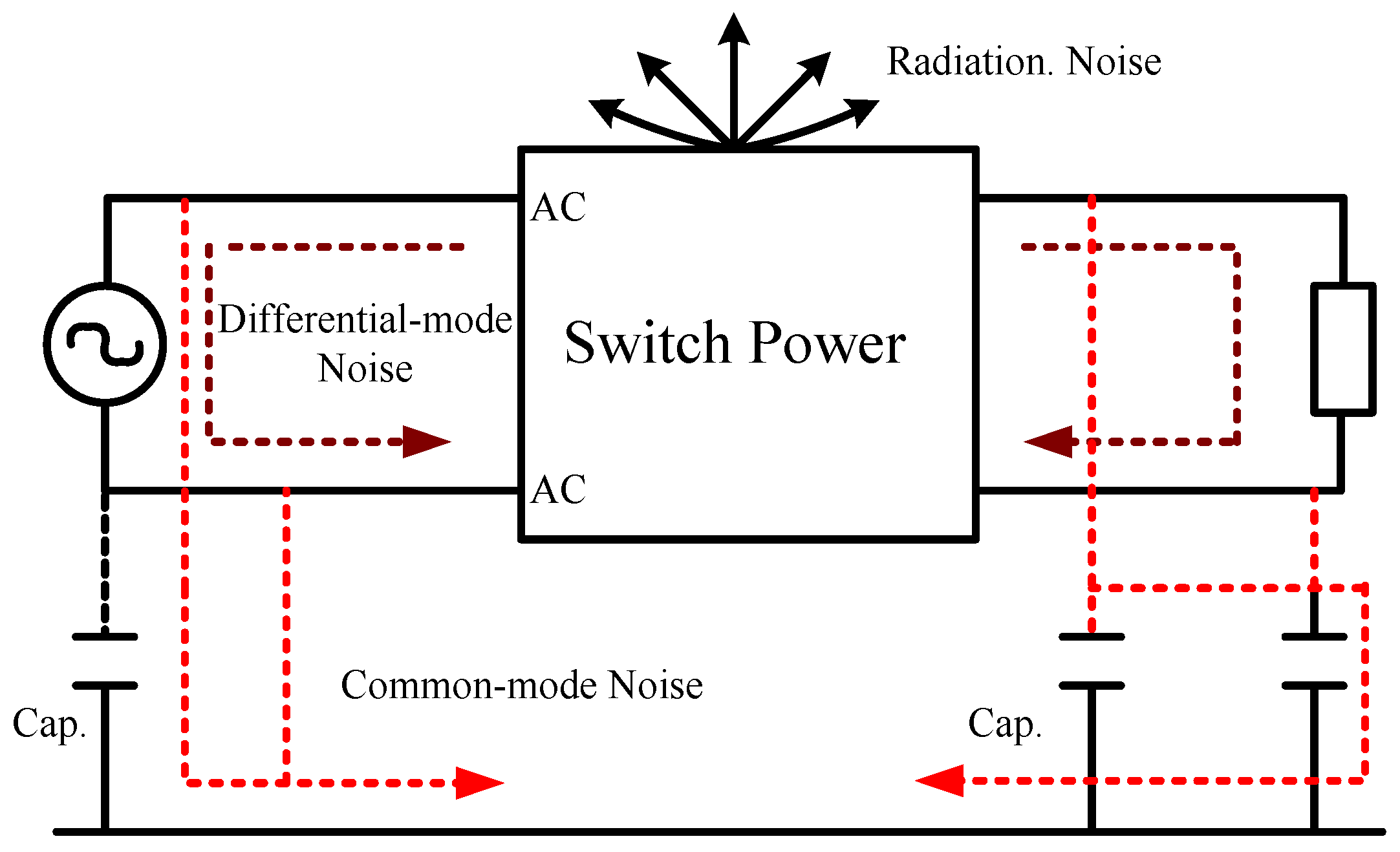
:1. Introduction
2. Literature Review
2.1. Experimental Study
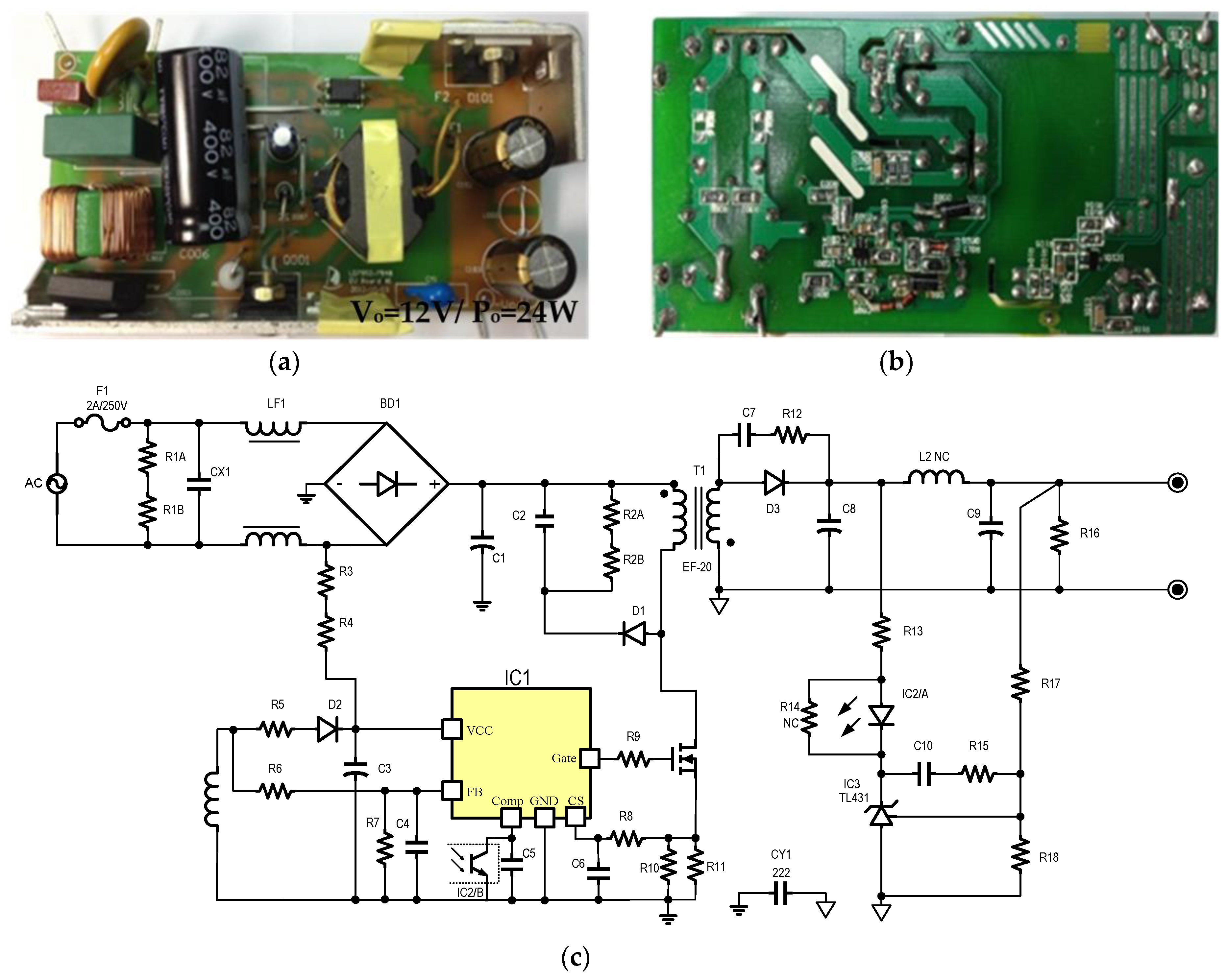
2.2. Commercial Product
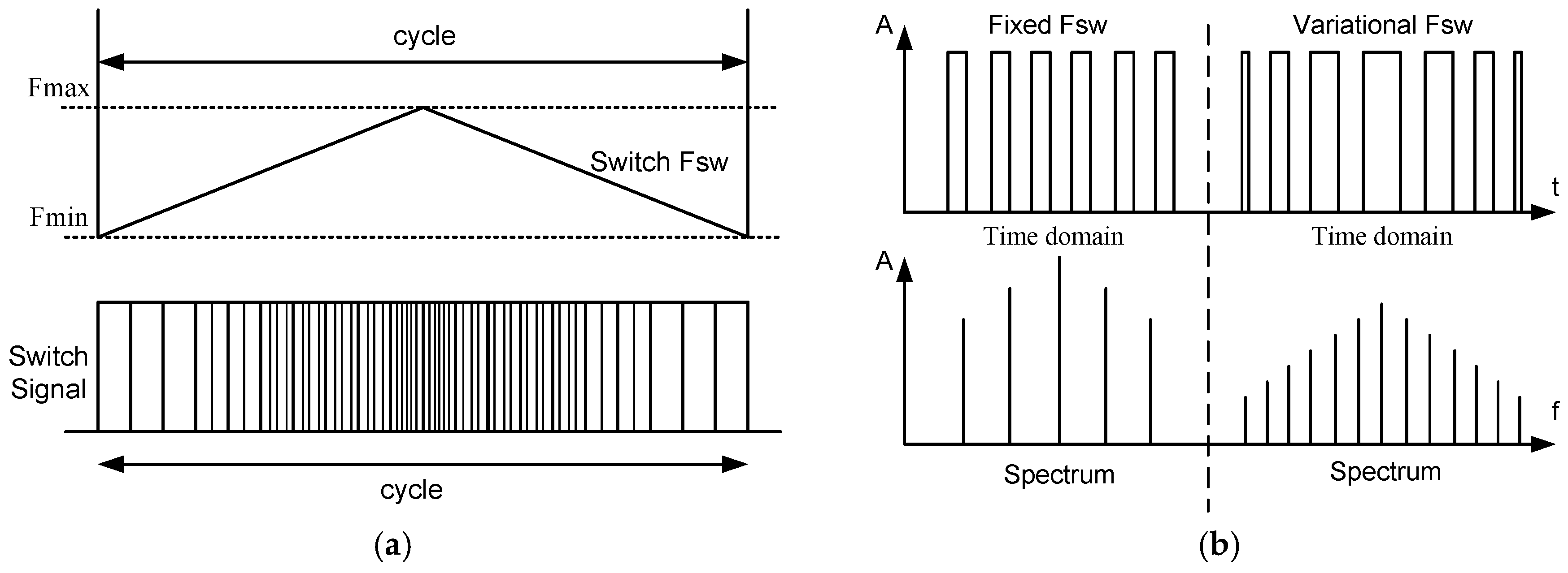
3. Frequency Modulation of Pulse-Width Module Signals
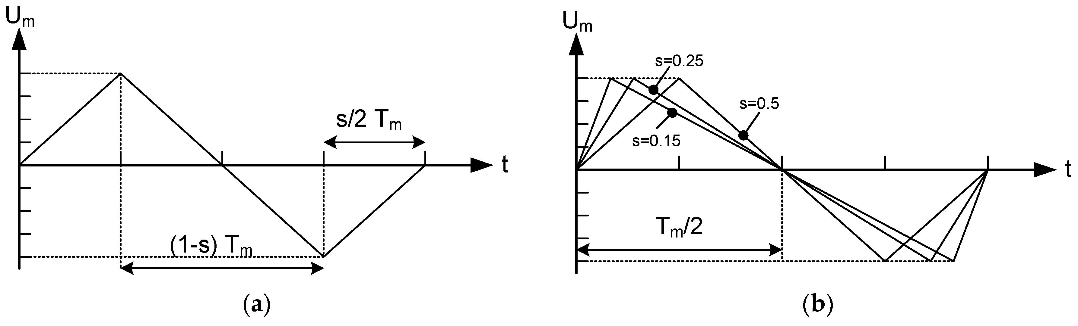
3.1. Single-Frequency Modulation of Pulse-Width Module Signals
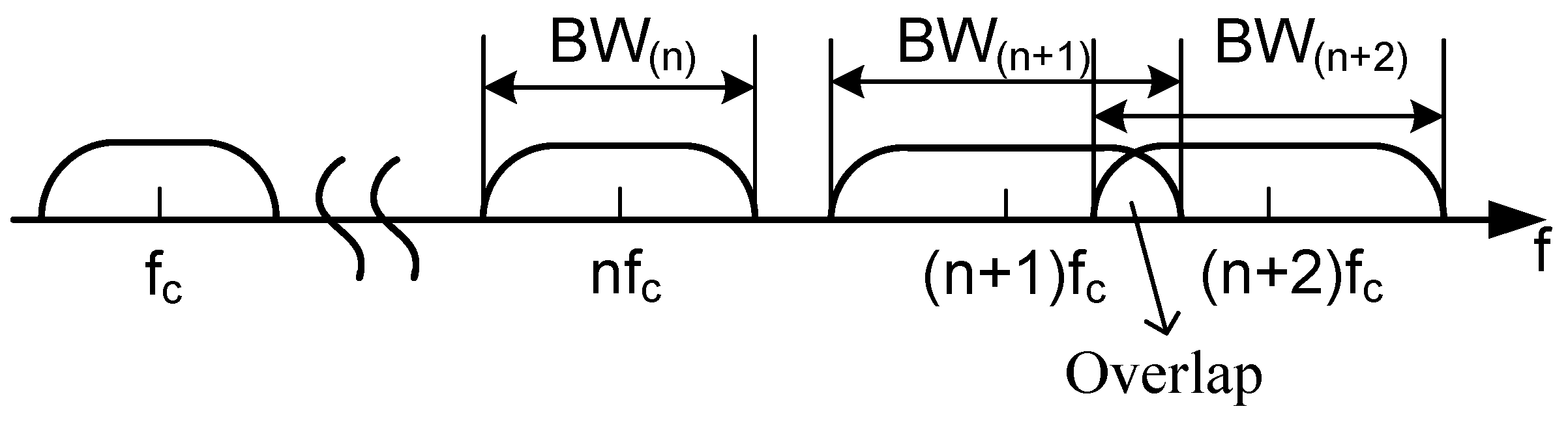
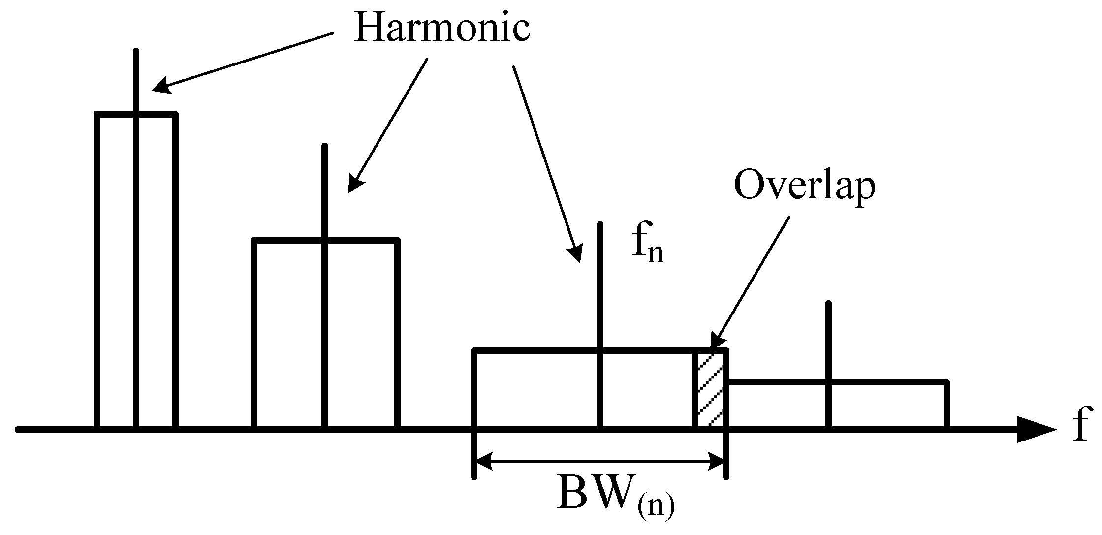
3.2. Calculation of High-Order Sub-Harmonic Superposition
- (1)
- Carrier frequency ωc shows an amplitude proportional to J0(mf1)J0(mf2).
- (2)
- Boundary frequency (ωc ± nΩ1) shows an amplitude proportional to Jn(mf1)J0(mf2).
- (3)
- Boundary frequency (ωc ± nΩ2) shows an amplitude proportional to J0(mf1)Jn(mf2).
- (4)
- Additional boundary frequency (combined frequency; ωc ± nΩ1 ± nΩ2) shows an amplitude proportional to Jn(mf1)J0(mf2), where n and p are random integers.
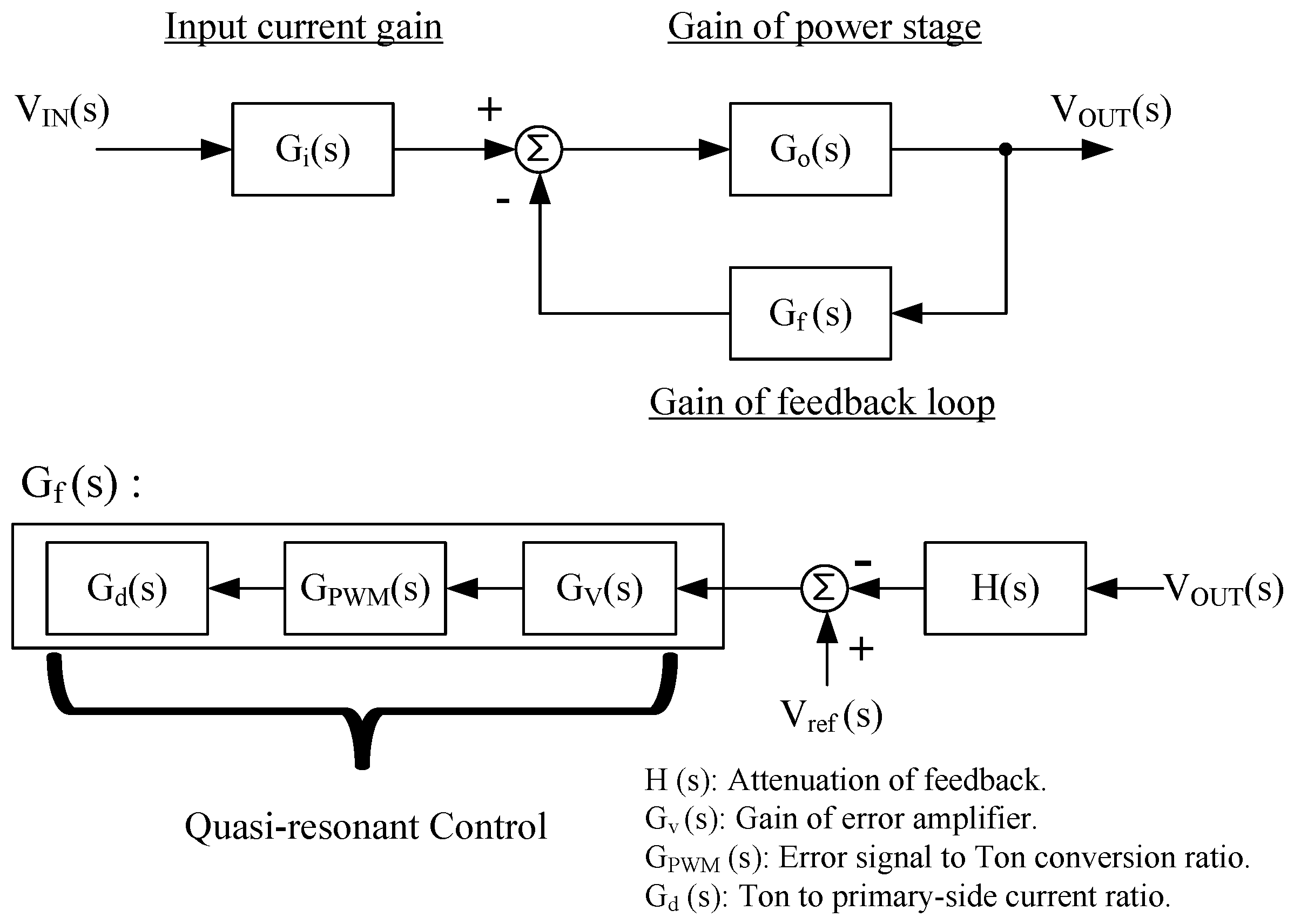
4. Design of Frequency Swapping Circuits
4.1. Selection and Analysis of Frequency Swapping Techniques
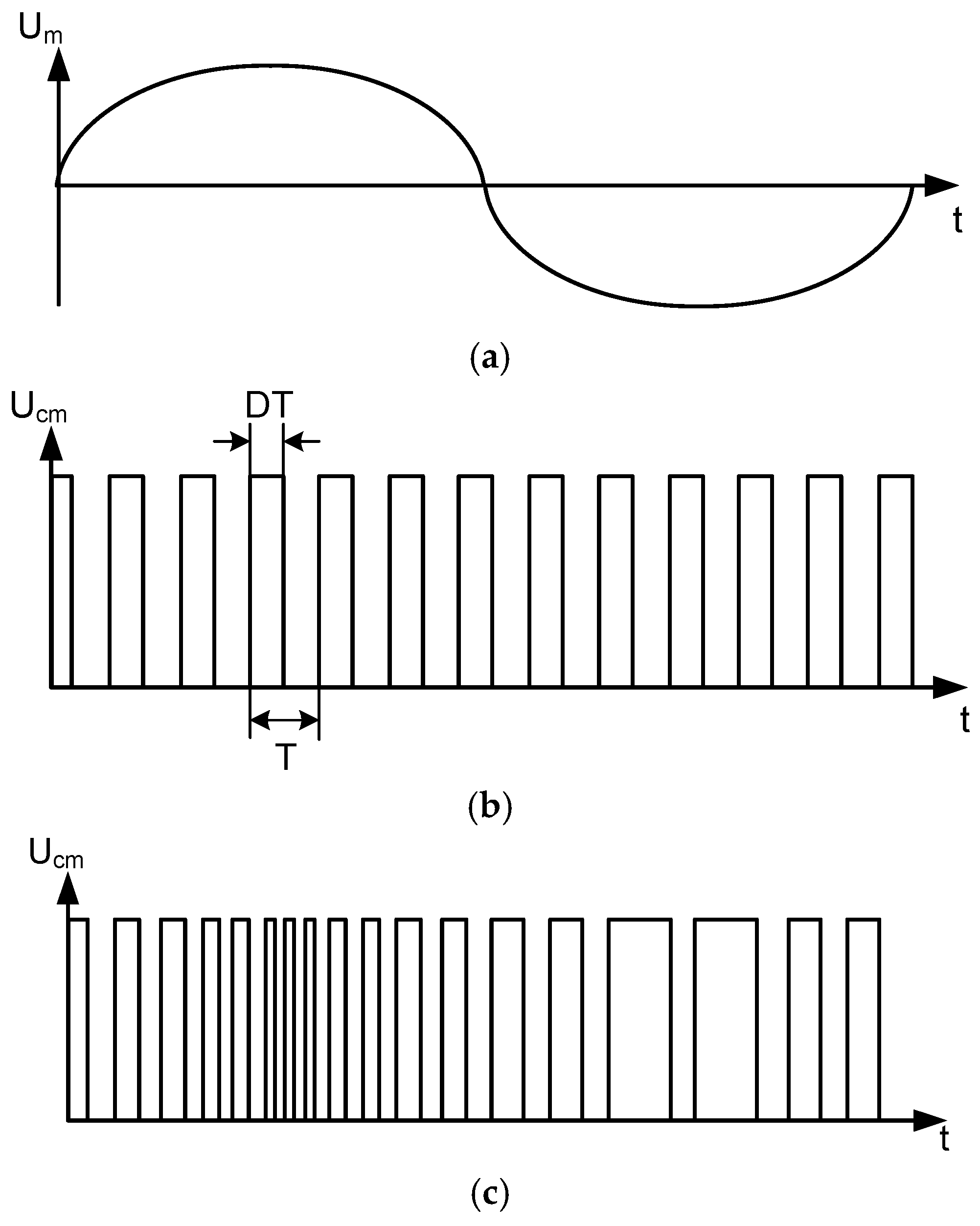
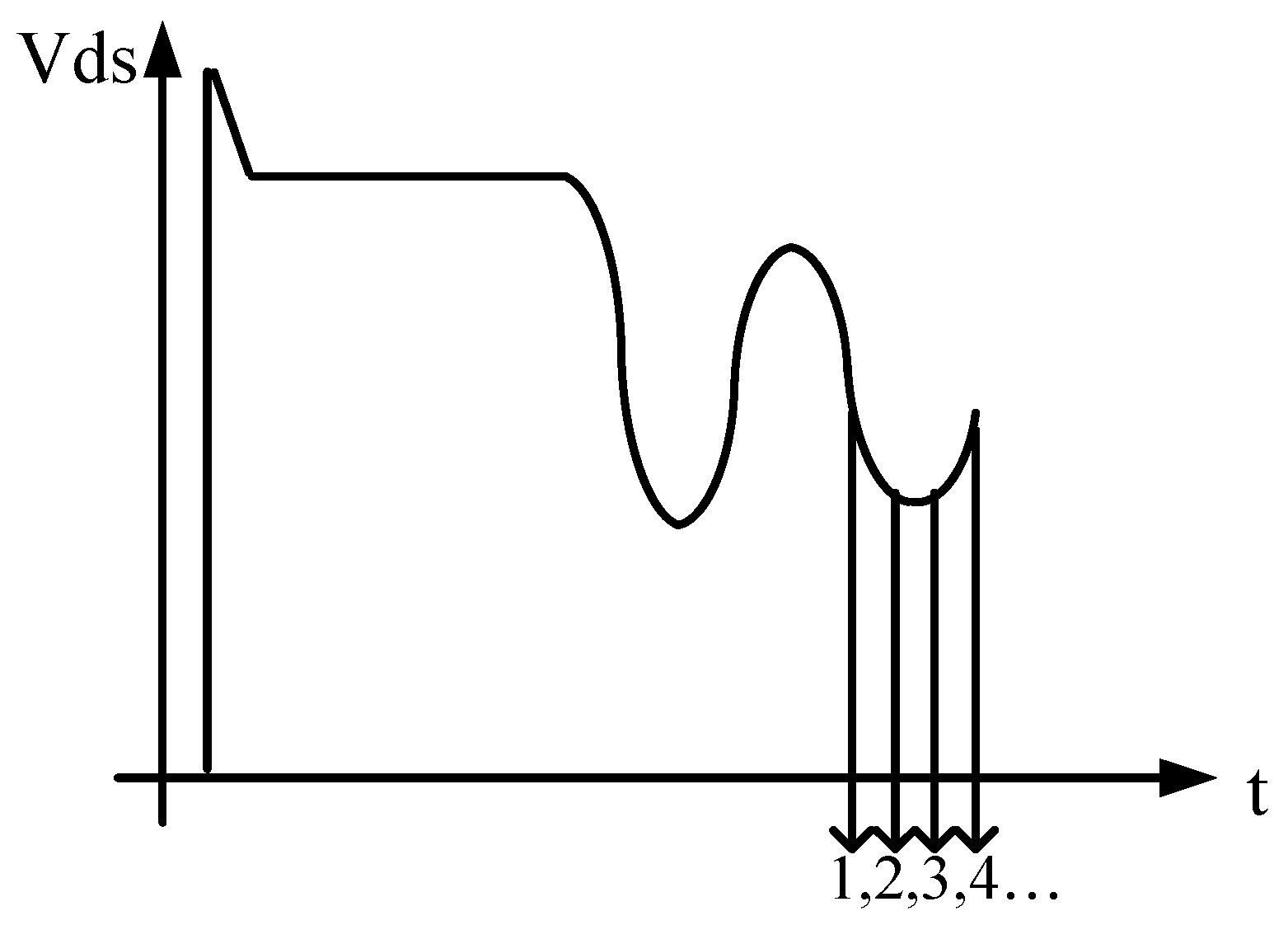
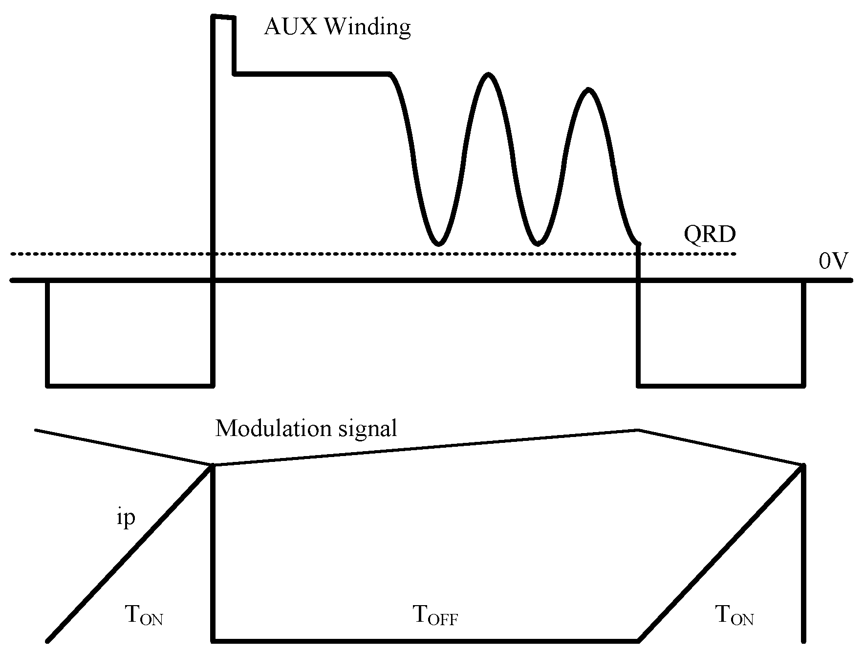
4.1.1. Change in Quasi-resonant Detection Delay Time
4.1.2. Change in Quasi-Resonant Flyback Valley Order
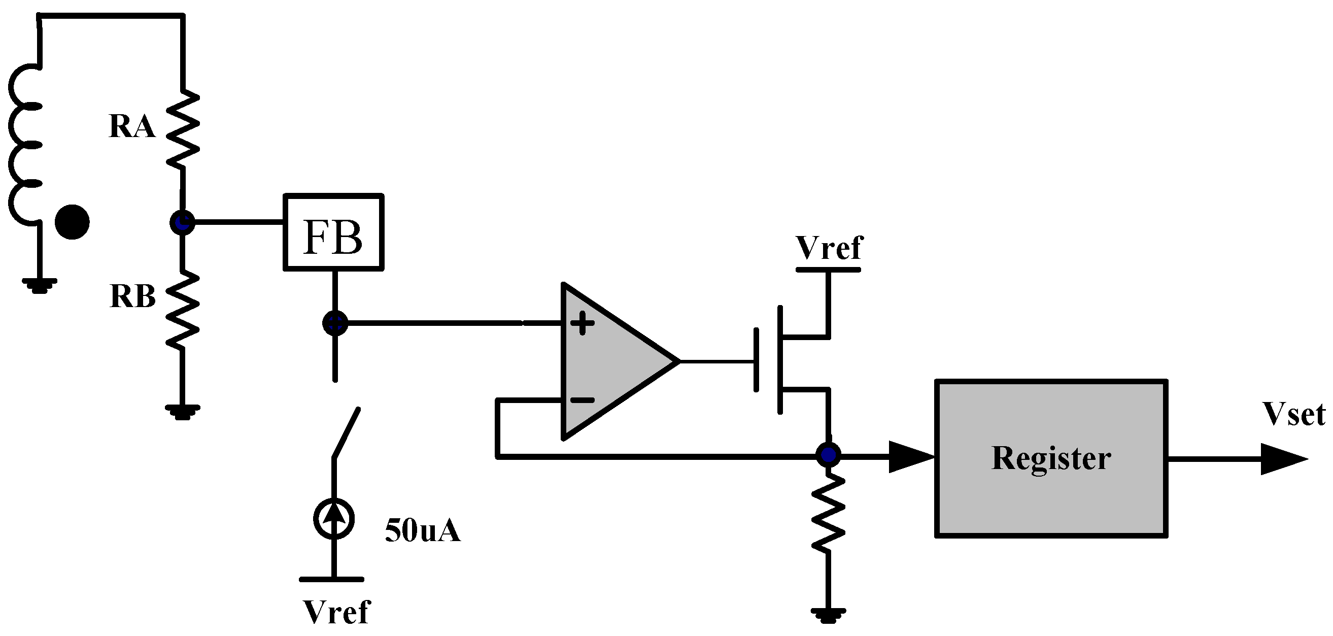
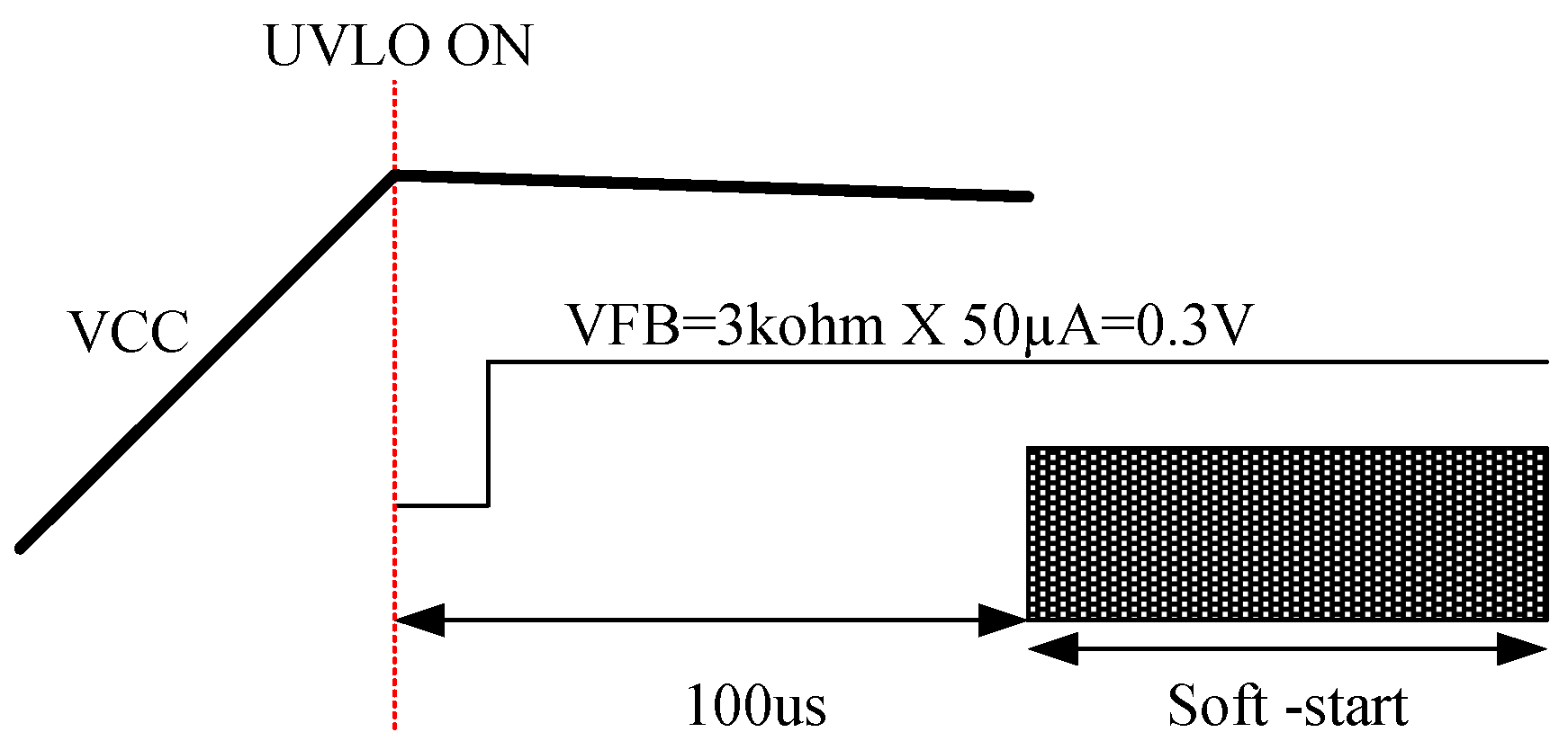
4.1.3. Disturbance on Voltage Feedback Signal
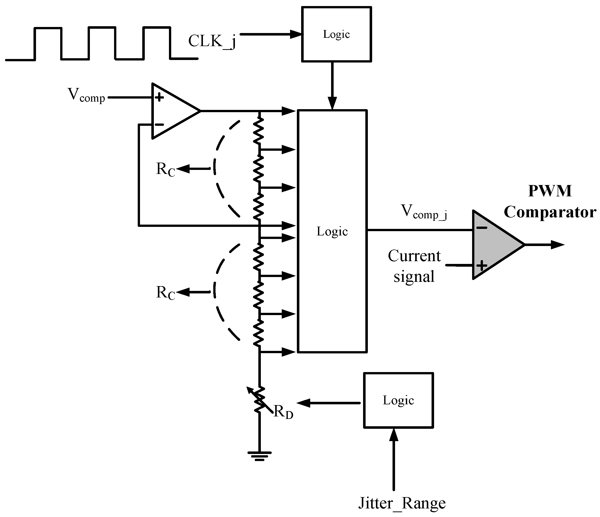
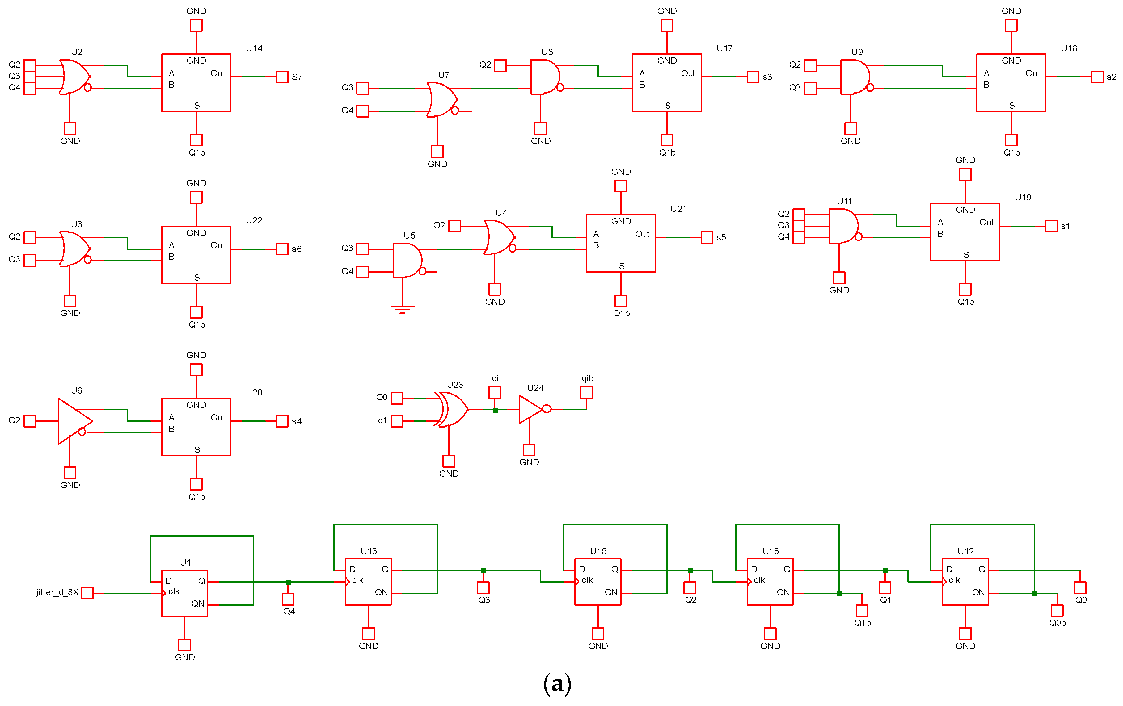
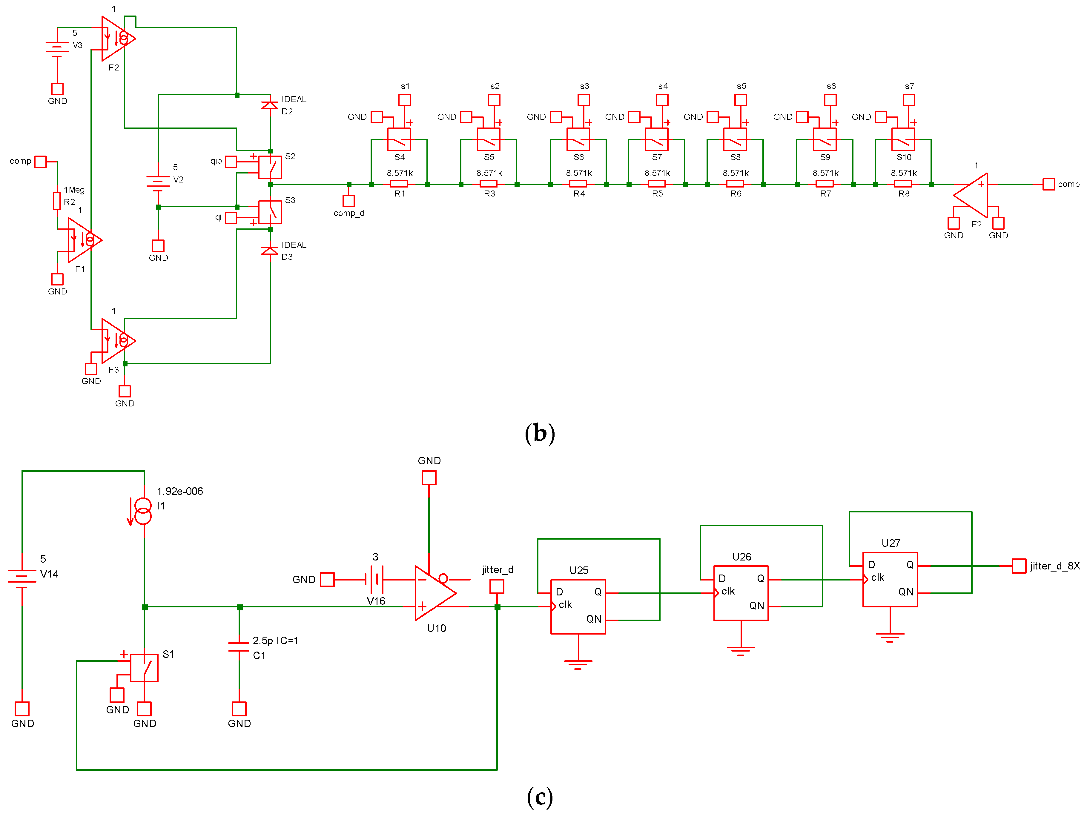
4.2. Embedded Logic Circuit of Adjustable Frequency Swapping
4.3. Embedded Logic Circuit of Feedback Disturbance
5. Results and Analysis
5.1. Simulation Results
- (1)
- When the frequency offset is too high, although the duty cycle remains unchanged, the corresponding component conduction time decreases. The Ton and Toff time occupy a major portion of duty cycle, thus hindering energy transmission. When the switching frequency is too low, the corresponding conduction time increases, which probably results in magnetic component saturation.
- (2)
- When the frequency offset is too high, energy transmission becomes uneven, which possibly induces large output ripples if the system cannot response this voltage feedback disturbance rapidly.
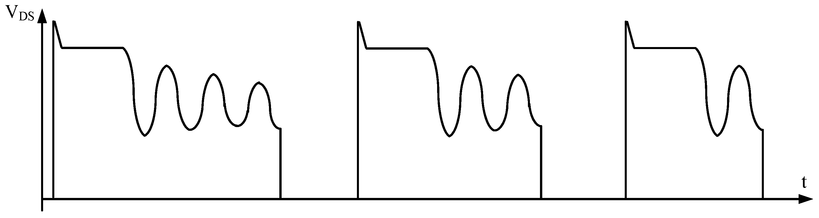
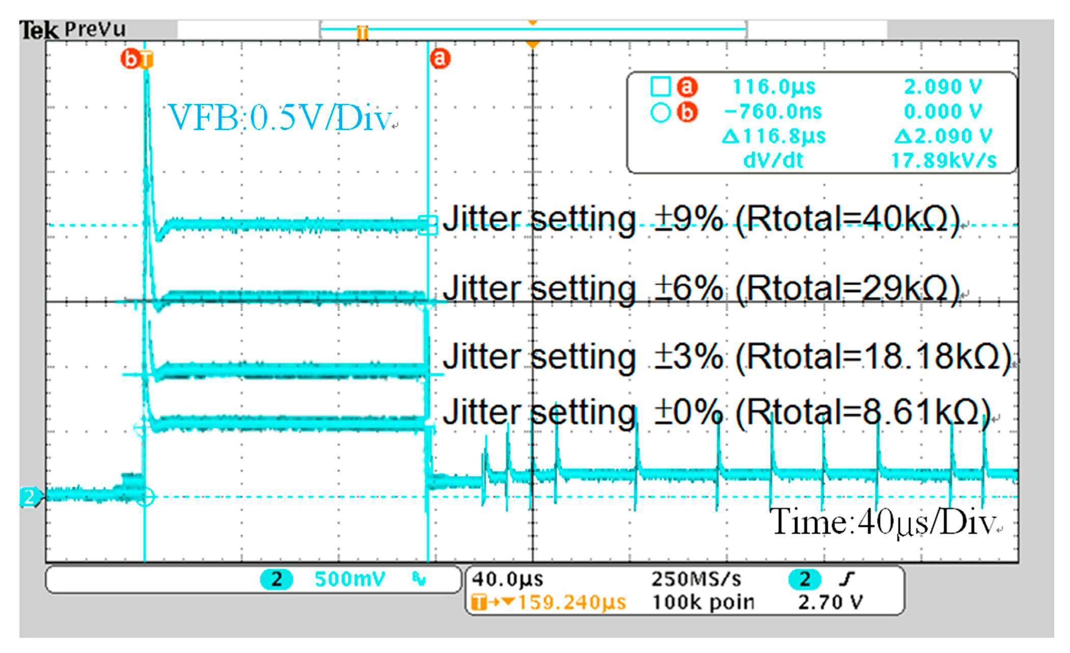
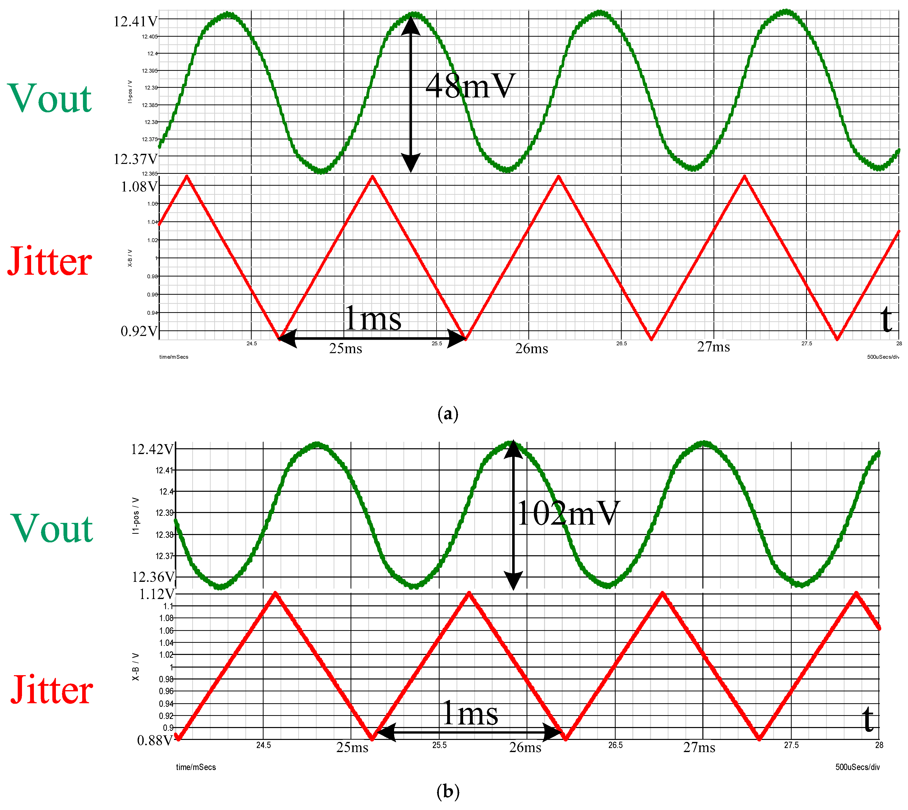
5.2. Waveform Measurement
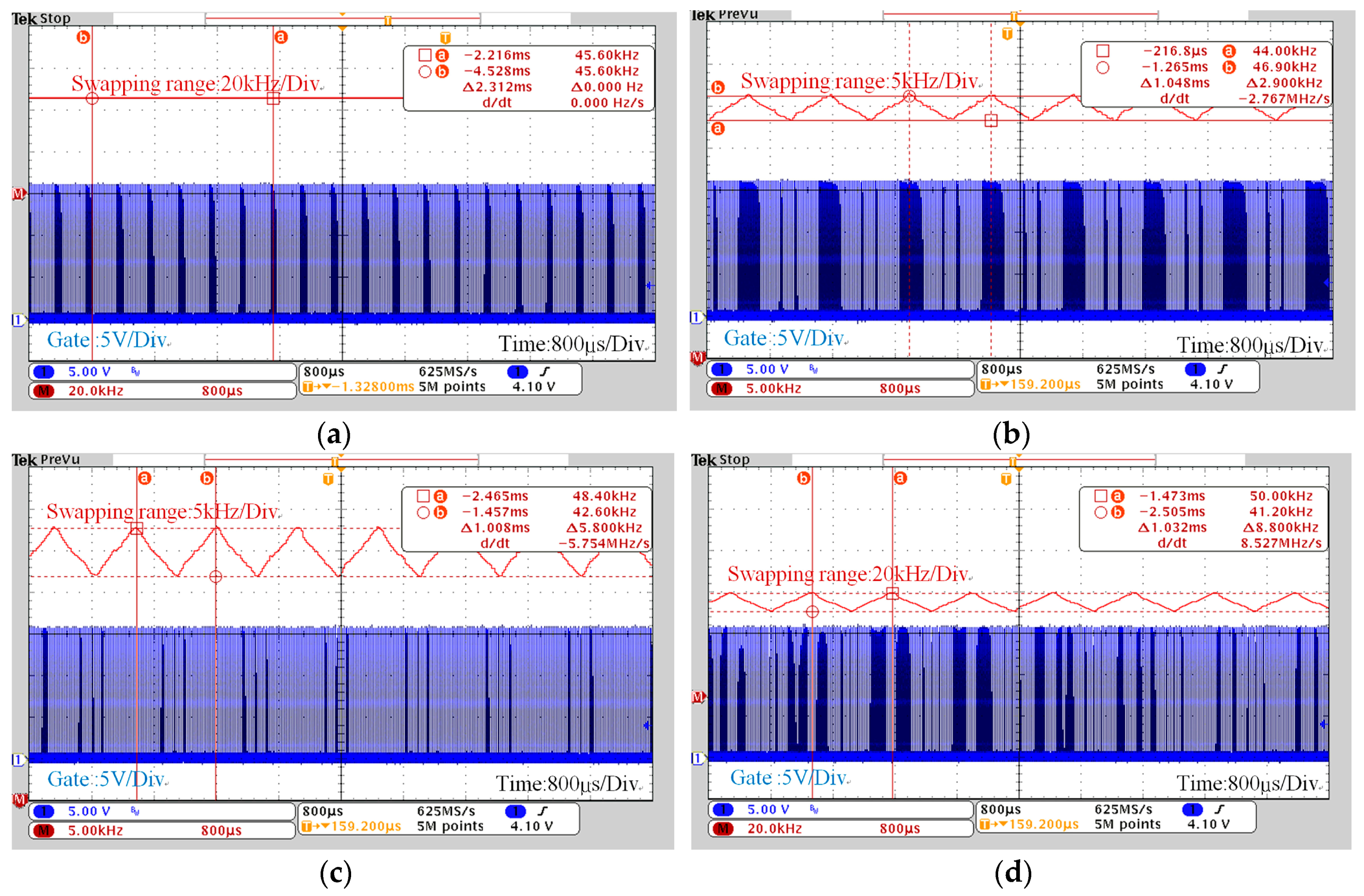
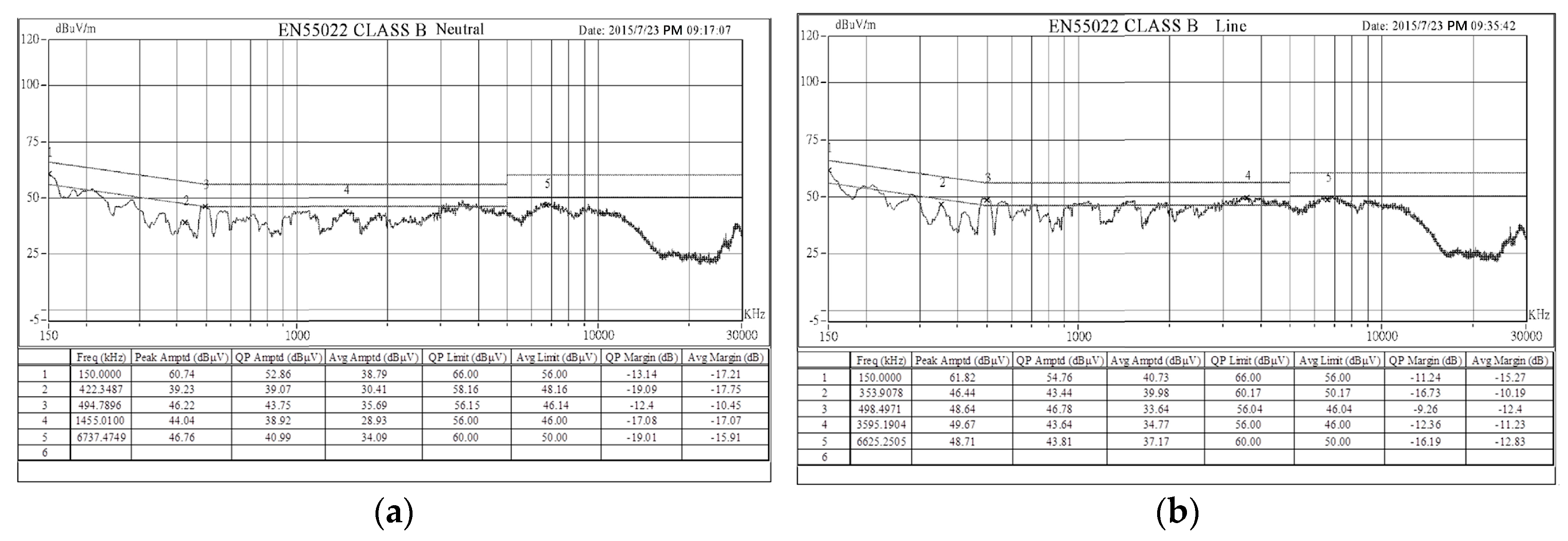
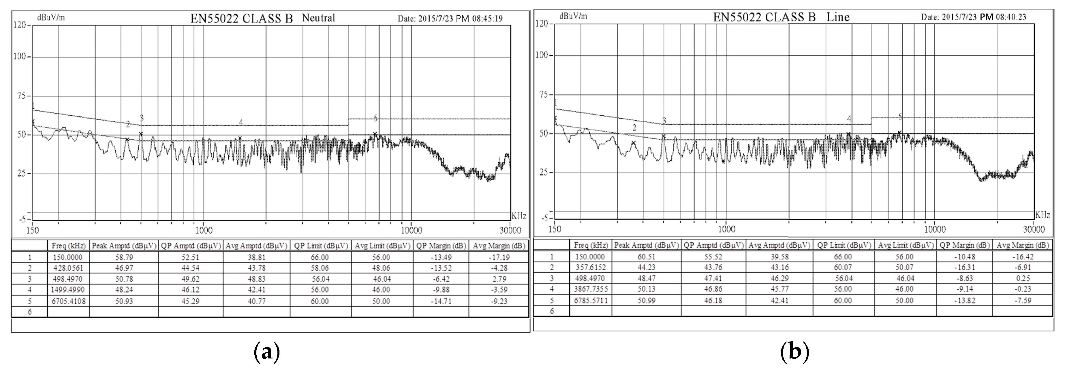
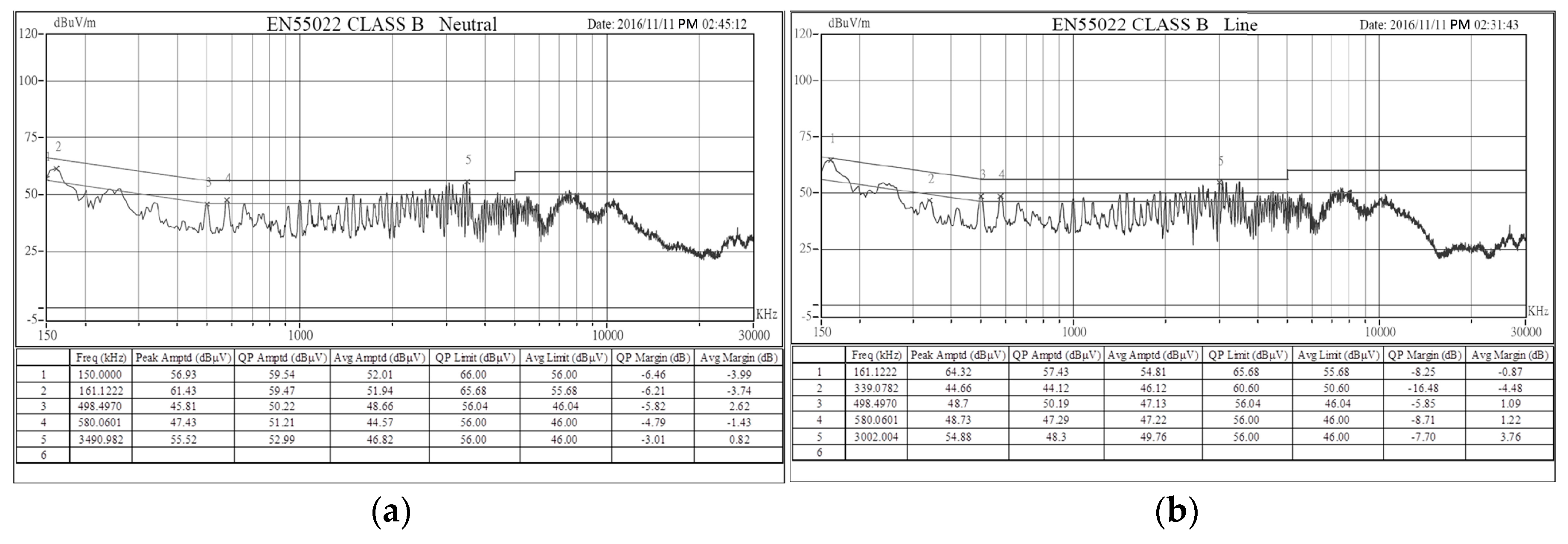
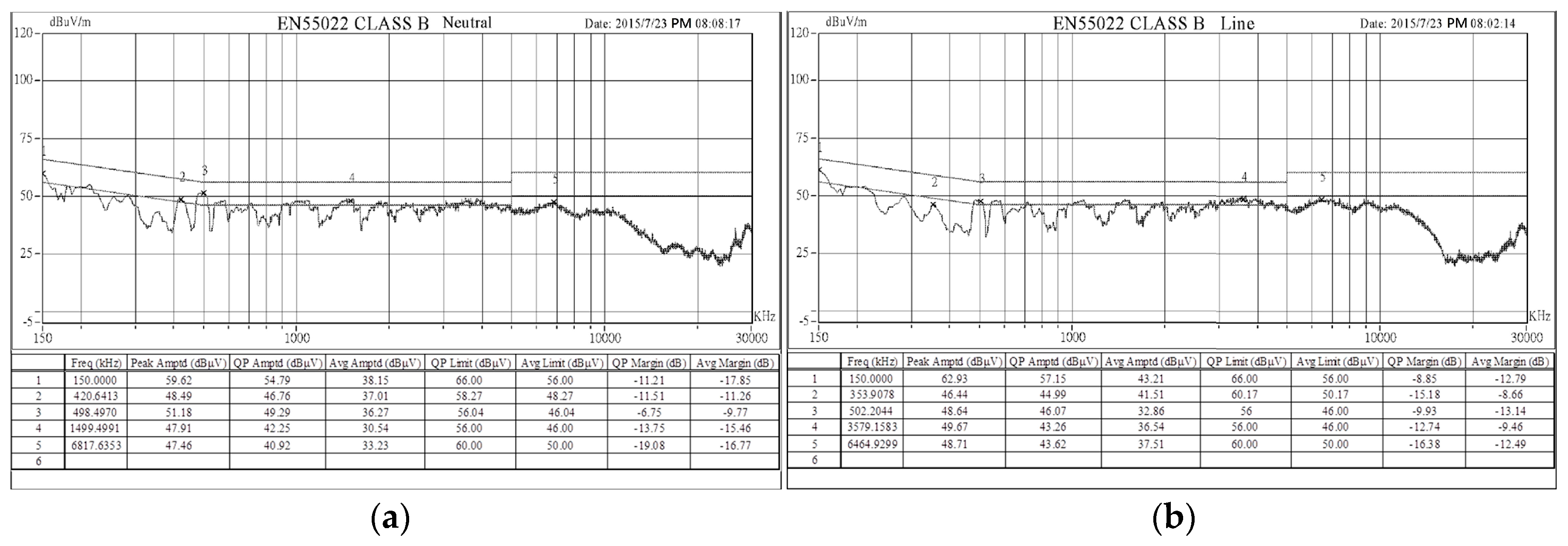
5.3. Testing Conducted Electromagnetic Interference
Comparison of Conducted Electromagnetic Interference with Distinct X-Capacitor Values
6. Conclusions
- (1)
- The novel frequency swapping technique can effectively reduce the EMI caused by the converters. EMI testing showed that the average (150 kHz to 10 MHz) margin was attenuated by approximately 13.24 dBμV.
- (2)
- The spectral distribution of the modulation wave is related to the slope of the modulation ratio. A well-performed spectral distribution is obtained by setting the swapping range to ±9%. When the spectrum of the modulation wave is non-modulated, there is no swapping frequency mechanism and vice versa. This pattern could be used to predict the spectral structures for the modulation waves of other shapes.
- (3)
- When close-loop oscillation and oscillation noise factors are considered, the switching frequency offset and modulation frequency should not be excessive. In the selection of the modulation parameters, the frequency offset must be determined first. The offset adopted in this experiment was approximately 9%, which caused zero abnormality in the original circuit.
- (4)
- Applying the novel frequency swapping technique can reduce the X-capacitor in the system π filter to 0.22 μF. The EN55022 standard was met regardless of testing the conducted EMI at the neutral or line ends. Both the QP and AVG amplitude margins were more than 6 dBμV. Thus, the proposed technique has the advantages of conserving the system components and reducing the layout area.
Acknowledgments
Author Contributions
Conflicts of Interest
References
- Wang, Y.-F.; Yang, L.; Wang, C.-S.; Li, W.; Qie, W.; Tu, S.-J. High step-up 3-phase rectifier with fly-back cells and switched capacitors for small-scaled wind generation systems. Energies 2015, 8, 2742–2768. [Google Scholar] [CrossRef]
- Arango, E.; Ramos-Paja, C.A.; Calvente, J.; Giral, R.; Serna, S. Asymmetrical interleaved DC/DC switching converters for photovoltaic and fuel cell applications—Part 1: Circuit generation, analysis and design. Energies 2012, 5, 4590–4623. [Google Scholar] [CrossRef]
- Karveis, G.A.; Manias, S.N. Analysis and design of a flyback zero-current switched (ZCS) quasi-resonant (QR) AC/DC converter. In Proceedings of the 27th Annual IEEE Power Electronics Specialists Conference, Baveno, Italy, 23–27 June 1996.
- Hsieh, P.C.; Chang, C.J.; Chen, C.L. A primary-side-control quasi-resonant flyback converter with tight output voltage regulation and self-calibrated valley switching. In Proceedings of the 2013 IEEE Energy Conversion Congress and Exposition, Denver, CO, USA, 15–19 September 2013.
- Wang, Z.; Wu, X.; Chen, M.; Zhang, J. Optimal design methodology for the current-sharing transformer in a quasi-resonant (QR) flyback LED driver. In Proceedings of the Twenty-Seventh Annual IEEE Applied Power Electronics Conference and Exposition, Orlando, FL, USA, 5–9 February 2012.
- Kuo, M.-T.; Tsou, M.-C. Simulation of standby efficiency improvement for a line level control resonant converter based on solar power systems. Energies 2015, 8, 338–355. [Google Scholar] [CrossRef]
- EN 55022, CISPR 22. Available online: http://www.rfemcdevelopment.eu/en/en-55022-2010 (accessed on 22 December 2016).
- González, D.; Gago, J.; Balcells, J. New simplified method for the simulation of conducted EMI generated by switched power converters. IEEE Trans. Ind. Electron. 2003, 50, 1078–1084. [Google Scholar] [CrossRef]
- Santolaria, A.; Balcells, J.; González, D. Theoretical and experimental results of power converter frequency modulation. In Proceedings of the IECON 02 IEEE 2002 28th Annual Conference of the Industrial Electronics Society, Seville, Spain, 5–8 November 2002.
- Lin, F.; Chen, D.Y. Reduction of power supply EMI emission by switching frequency modulation. IEEE Trans. Power Electron. 1994, 9, 132–137. [Google Scholar]
- Paul, C.R. Transmission Lines in Digital Systems for EMC Practitioners; Wiley: Hoboken, NJ, USA, 2012. [Google Scholar]
- Zhang, D.; Chen, D.; Sable, D. Non-intrinsic differential mode noise caused by ground current in an off-line power supply. In Proceedings of the 29th Annual IEEE Power Electronics Specialists Conference, PESC 98 Record, Fukuoka, Japan, 22–22 May 1998; pp. 1131–1133.
- Kchikach, M.; Yuan, Y.S.; Qian, Z.M.; Pong, M.H. Simple modeling for conducted common-mode current in switching circuits. In Proceedings of the PESC Record—IEEE 32nd Annual Power Electronics Specialists Conference, Vancouver, BC, Canada, 17–22 June 2001.[Green Version]
- Kuisma, M. Variable frequency switching in power supply EMI-control: An overview. IEEE Aerosp. Electron. Syst. Mag. 2003, 18, 18–22. [Google Scholar] [CrossRef]
- Maillet, Y.; Lai, R.; Wang, S.; Wang, F.; Burgos, R.; Boroyevich, D. High-density EMI filter design for dc-fed motor drives. IEEE Trans. Power Electron. 2010, 25, 1163–1172. [Google Scholar] [CrossRef]
- Ala, G.; Giaconia, G.C.; Giglia, G.; Di Piazza, M.C.; Luna, M.; Vitale, G.; Zanchetta, P. Computer aided optimal design of high power density EMI filters. In Proceedings of the 2016 IEEE 16th International Conference on Environment and Electrical Engineering, Florence, Italy, 6–8 June 2016.
- Ala, G.; Di Piazza, M.C.; Giaconia, G.C.; Giglia, G.; Vitale, G. Design and performance evaluation of a high power-density emi filter for PWM inverter-fed induction-motor drives. IEEE Trans. Ind. Appl. 2016, 52, 2397–2404. [Google Scholar] [CrossRef]
- Touré, B.; Schanen, J.L.; Gerbaud, L.; Meynard, T.; Roudet, J.; Ruelland, R. EMC modeling of drives for aircraft applications: Modeling process, EMI filter optimization, and technological choice. IEEE Trans. Power Electron. 2013, 28, 1145–1156. [Google Scholar] [CrossRef]
- Hardin, K.B.; Fessler, J.T.; Bush, D.R. A study of the interference potential of spread spectrum clock generation techniques. In Proceedings of the IEEE International Symposium on Electromagnetic Compatibility, Atlanta, GA, USA, 14–18 August 1995.
- TOP242-TOP250 Reference Design. Available online: http://chinese.powerint.com/dak.zh-cn.html (accessed on 8 March 2016).
- LTC6902 Datasheet. Available online: http://datasheet.eeworld.com.cn/pdf/28512_LINER_LTC6902.html (accessed on 9 August 2016).
- NCP1215A Datasheet. Available online: http://datasheet.eeworld.com.cn/pdf/12824_ONSEMI_NCP1215.html (accessed on 9 August 2016).
- ICE3B0365J Datasheet. Available online: http://datasheet.eeworld.com.cn/pdf/151232_INFINEON_ICE3B0365J.html (accessed on 9 August 2016).
- FSDH0265 Series Datasheet. Available online: http://datasheet.eeworld.com.cn/pdf/37029_FAIRCHILD_FSDH0265RL.html (accessed on 9 August 2016).
- Sendra, J.B.I. SSCG Methods of EMI Emission Reduction applied to Switching Power Converters. Ph.D. Thesis, BarcelonaTech, Barcelona, Spain, 2004. [Google Scholar]


| Ideal Rtotal | VFB Range | Suggested Rtotal Value | Swapping Range (%) |
|---|---|---|---|
| 40 k < Rtotal | 1.7 < VFB | 42 k | ±9 |
| 22 k < Rtotal < 40 k | 1.1 < VFB < 1.7 | 30 k | ±6 |
| 14 k < Rtotal < 22 k | 0.7 < VFB < 1.1 | 20 k | ±3 |
| Rtotal < 14 k | VFB < 0.7 | 10 k | ±0 |
| Hardware/Simulation Parameters | Specifications |
|---|---|
| Input Voltage | Vin = 90 V–264 V |
| Output Voltage | Vo = 12 V |
| Output Current | Io = 0–2 A |
| Switch Frequency | fs = 65 kHz |
| Max. Duty Cycle | Dmax = 0.48 |
| Transformer | Lp = 1.6 mH |
| Ratio of Transformer | Nm = 0.8 |
| Output Capacitance | Co = 680 uF × 2; ESR = 0.01 ohm |
| X-Capacitor Value | Comparison of Swapping Range Settings | Frequency Swapping Ratio | Frequency Swapping Period | Output Ripple | |
|---|---|---|---|---|---|
| 90 V/60 Hz | 264 V/50 Hz | ||||
| 0.22 µF | 8.61 kΩ | ±0% | 1 ms | Δ3 mV | Δ5.2 mV |
| 18.18 kΩ | ±3% | 1 ms | Δ21 mV | Δ41 mV | |
| 29 kΩ | ±6% | 1 ms | Δ32 mV | Δ71 mV | |
| 40 kΩ | ±9% | 1 ms | Δ48 mV | Δ98 mV | |
| 52 kΩ | ±12% | 1 ms | Δ102 mV | Δ143 mV | |
| Items | Frequency | QP Limit | Average Limit | QP Margin | Average Margin | |
|---|---|---|---|---|---|---|
| kHz | dBμV | dBμV | dB | dB | ||
| X-capacitor of 0.33 μF (fixed frequency) | Neutral | 428.0561 | 58.06 | 48.06 | −13.52 | −4.28 |
| 498.4970 | 56.04 | 46.04 | −6.42 | 2.79 | ||
| Line | 357.6152 | 60.07 | 50.07 | −16.31 | −6.91 | |
| 498.497 | 56.04 | 46.04 | −8.63 | 0.25 | ||
| X-capacitor of 0.33 μF (±9% frequency swapping) | Neutral | 422.3487 | 58.16 | 48.16 | −19.09 | −17.75 |
| 494.7896 | 56.15 | 46.14 | −12.4 | −10.45 | ||
| Line | 353.9078 | 60.17 | 50.17 | −16.73 | −10.19 | |
| 498.4971 | 56.04 | 46.04 | −9.26 | −12.4 | ||
| X-capacitor of 0.22 μF (fixed frequency) | Neutral | 498.4970 | 45.81 | 50.22 | −5.82 | 2.62 |
| 580.0601 | 47.43 | 51.21 | −4.79 | −1.43 | ||
| Line | 339.0782 | 44.66 | 44.12 | −16.48 | −4.48 | |
| 498.4970 | 48.7 | 50.19 | −5.85 | 1.09 | ||
| X-capacitor of 0.22 μF (±9% frequency swapping) | Neutral | 420.6413 | 58.27 | 48.27 | −11.51 | −11.26 |
| 498.497 | 56.04 | 46.04 | −6.75 | −9.77 | ||
| Line | 353.9078 | 60.17 | 50.17 | −15.18 | −8.66 | |
| 502.2044 | 56 | 46 | −9.93 | −13.14 | ||
© 2016 by the authors; licensee MDPI, Basel, Switzerland. This article is an open access article distributed under the terms and conditions of the Creative Commons Attribution (CC-BY) license (http://creativecommons.org/licenses/by/4.0/).
Share and Cite
Kuo, M.-T.; Tsou, M.-C. Novel Frequency Swapping Technique for Conducted Electromagnetic Interference Suppression in Power Converter Applications. Energies 2017, 10, 24. https://doi.org/10.3390/en10010024
Kuo M-T, Tsou M-C. Novel Frequency Swapping Technique for Conducted Electromagnetic Interference Suppression in Power Converter Applications. Energies. 2017; 10(1):24. https://doi.org/10.3390/en10010024
Chicago/Turabian StyleKuo, Ming-Tse, and Ming-Chang Tsou. 2017. "Novel Frequency Swapping Technique for Conducted Electromagnetic Interference Suppression in Power Converter Applications" Energies 10, no. 1: 24. https://doi.org/10.3390/en10010024