
Partial Stray Inductance Modeling and Measuring of Asymmetrical Parallel Branches on the Bus-Bar of Electric Vehicles


School of Electrical and Power Engineering, China University of Mining and Technology, Xuzhou 221116, China
*
Author to whom correspondence should be addressed.
Energies 2017, 10(10), 1519; https://doi.org/10.3390/en10101519
Submission received: 16 August 2017
/
Revised: 13 September 2017
/
Accepted: 26 September 2017
/
Published: 1 October 2017
(This article belongs to the Special Issue Advances in Electric Vehicles and Plug-in Hybrid Vehicles 2017)
Abstract
:In order to increase the power rating of electric vehicles, insulated gate bipolar translator (IGBT) modules with multiple power terminals are usually adopted. The transient current sharing of the same polarity power terminals is related to the stray inductance in the branches of the bus-bar. Based on the laminated bus-bar of a three-phase inverter in the electric vehicles that consists of asymmetrical parallel branches, this paper investigates the transient current imbalance sharing caused by the asymmetrical stray inductance in the parallel branches of the bus-bar from the view of energy storing and releasing of stray inductance for the first time. Besides, the partial self-inductance and mutual-inductance model of the parallel branches is set up. Finally, a high-precision partial stray inductance measurement method is proposed, and the accuracy of the partial stray inductance model for asymmetrical parallel branches is verified by experimental tests.
1. Introduction
In recent years, electrical vehicles (EVs) have gained unprecedented evolution in consideration of the current energy crisis and environmental protection [1]. For an EV inverter, high efficiency, high power density, low harmonics, small volume, and low cost are essential [2,3,4]. Due to the low stray inductance, the laminated bus-bar has now been widely used in power electronics and converter products [5,6,7]. With power devices continuing to move upwards in current levels and switching frequency, laminated bus-bars have been attracting increasing interest from both industry and academia for the system benefits they exhibit [8]. The over-voltage spikes across the semiconductor during switching directly results from the commutation loop stray inductance. The high di/dt values produced during commutations by these new fast switching devices and diodes are currently the main source of conducted and radiated noise emissions, which usually interferes with nearby equipment through conduction or radiation [9,10]. For an EV inverter, the position of the small signal control circuit is often very close to high voltage, large current components such as the bus-bar or the power devices considering the limited space in an enclosure. The strength of Electro Magnetic Interference (EMI) emission is associated with transient current distribution on the bus-bar. So, for reliable operation of the control circuit in an EV inverter, the analysis, extraction, and evaluation of the stray inductance for a laminated bus-bar are very important.
Due to the increasing power of EV inverters, IGBT modules with multiple power terminals are often adopted. Moreover, the transient current sharing performance between power terminals of the same polarity is related to the stray inductance of the branches. In prior research, the most focus has been on optimizing the bus-bar structure based on the circuit topology [6,7,11]. Partial inductance theory is applied to build the model of bus-bar stray inductance [12,13,14]. The Partial Element Equivalent Circuit (PEEC) method [15,16] is adopted to construct the model and investigate the transient current distribution in the laminated bus-bar. Furthermore, with consideration of the current path, a partial self-inductance and mutual-inductance model of a H-bridge bus-bar has been built [17]. All the modeling and analysis are based on a single power electronics topology. But, the transient imbalance current sharing caused by the asymmetrical stray inductance in bus-bar parallel branches is comparatively scarce. This paper deeply investigates the transient imbalance current sharing arising from the asymmetrical stray inductance in bus-bars from the view of stray energy storing and releasing for the first time. The partial self-inductance and mutual-inductance model of the asymmetrical parallel branches is also set up to facilitate transient current analysis.
In order to evaluate the stray inductance of the bus-bar and verify the modeling accuracy, many measuring methods have been proposed by scholars and engineers. These include gap voltage measurement based on the IGBT turn-on process [18], time domain reflectometry (TDR) method [19], resonant capacitance measurement methods [6], stray inductance integral arithmetic extraction method for bus-bar based on turn-on/off transient process [20], network analyzer measurement [17], etc. However, all these methods mentioned above focus on the total stray inductance of the current communication loops rather than the partial inductance. This paper proposes a high precision method to measure the partial inductance in the bus-bar, and the measuring accuracy is also analyzed considering the spatial transient electromagnetic field. Experimental evaluation of partial stray inductance extraction including direct and indirect measurement verifies the proposed model and measuring method.
2. Inverter Layout and Equivalent Circuit of the Bus-Bar
2.1. Inverter Layout Consideration
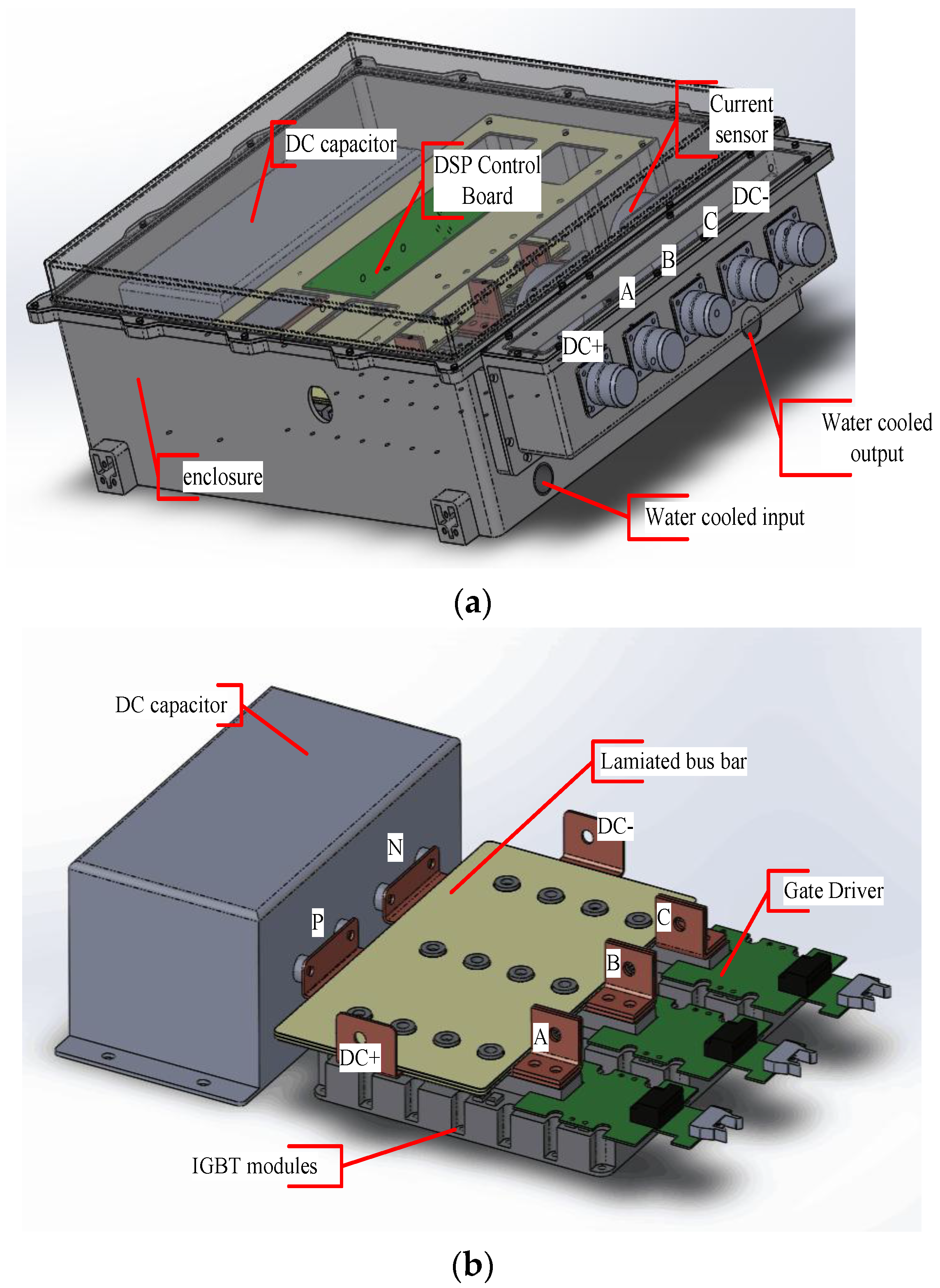
The main drivers for the development of EVs can be summarized to be cost, power density, specific volume, efficiency, and reliability. In this design, the power rating of the EV inverter is 200 kW. The inverter is assembled using individual building blocks serving the system, including switch (power device IGBT), energy storage (DC link capacitor), current distributor (copper bus-bar structure), and cooling system (liquid cooled heat sink). In addition, sensor functions (Hall elements) and control circuits are integrated. This setup is connected using screws and is supported by mechanical parts and protected by an enclosure, which is shown in Figure 1a. The inner structure of the inverter is shown in Figure 1b, in which the 1.2-KV/1400-A half bridge IGBT module is used. A low-inductance, high-frequency film capacitor is used to replace the conventional electrolytic bulk capacitors to reduce size and enhance the reliability.
High-speed switching devices produce lots of EMI noise during the fast on-off process, which usually interferes with nearby equipment through conduction or radiation [8,9,10]. Typical problems caused are measurement errors in sensors, false control signals, and interference in the gate voltages of switching devices [8]. Excessive noise can deteriorate control, reduce efficiency, and cause malfunctions of system. In this design, the control circuit is on the topside of the bus-bar. High impedance circuits are sensitive to EMI, such as the signal conditioning circuit of analog to digital (AD) acquisition. The source of EMI is associated with the transient current changes in the bus-bar. Simulation plays an important role in understanding the operating principle of the whole system and the functioning of some key components because it is more instructive and can save time and cost. Previous simulation platforms only concern analysis of the control algorithm. Parasitic elements are usually omitted to save simulation time [21]. So, in order to predict and evaluate the EMI/Electro Magnetic Compatibility (EMC) performance accurately and to further guide the layout of some key components in a limited space for EV inverters, a precise simulation platform that includes the main parasitic components should be built up.
2.2. Equivalent Circuit of Bus-bar Considering Stray Inductance
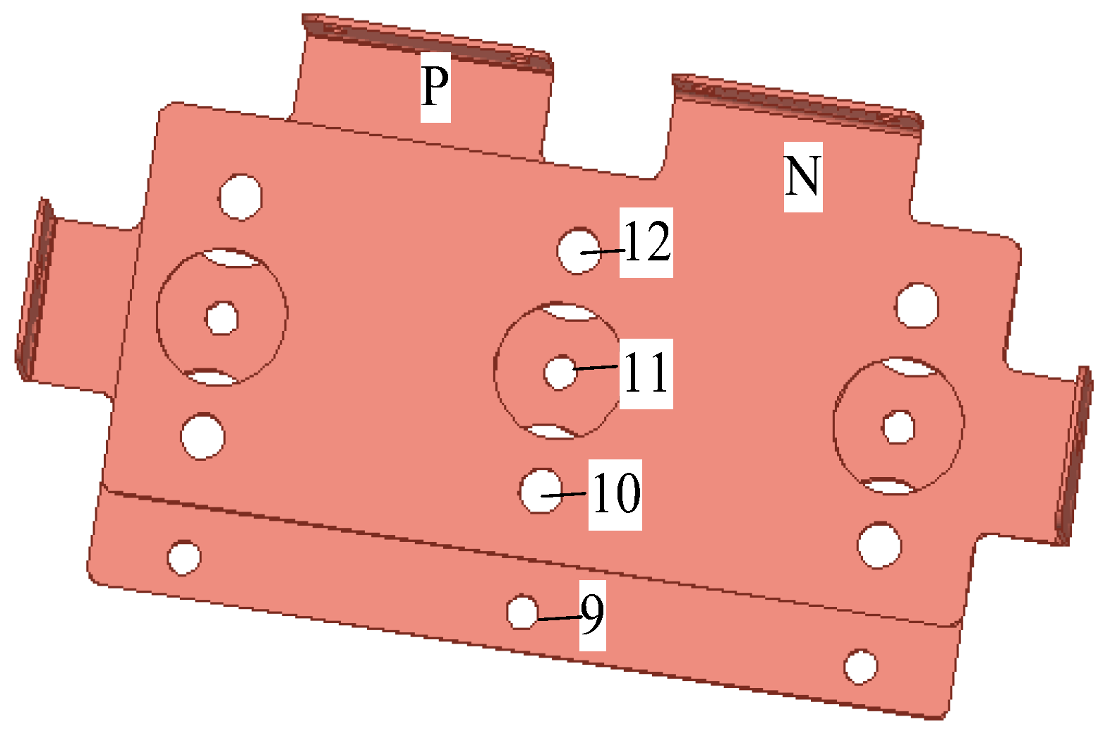
The structure and circuit principle of the half bridge IGBT module adopted in this design is shown in Figure 2. There are 5 power terminals on the IGBT, terminals 9 and 11 represent collector of the upper IGBT, terminals 10 and 12 represent emitter of the lower IGBT and terminal 8 represents the middle terminal.
The detailed structure of the laminated bus-bar is shown in Figure 3. The power terminal P and N are connected to the anode and cathode of the DC bus capacitor. A, B, and C are the output terminals of the inverter. The power terminals 9 and 11 on the positive bus are connected to the Collector of the upper IGBT. The power terminals 10 and 12 on the negative bus are connected to the Emitter of the lower IGBT.
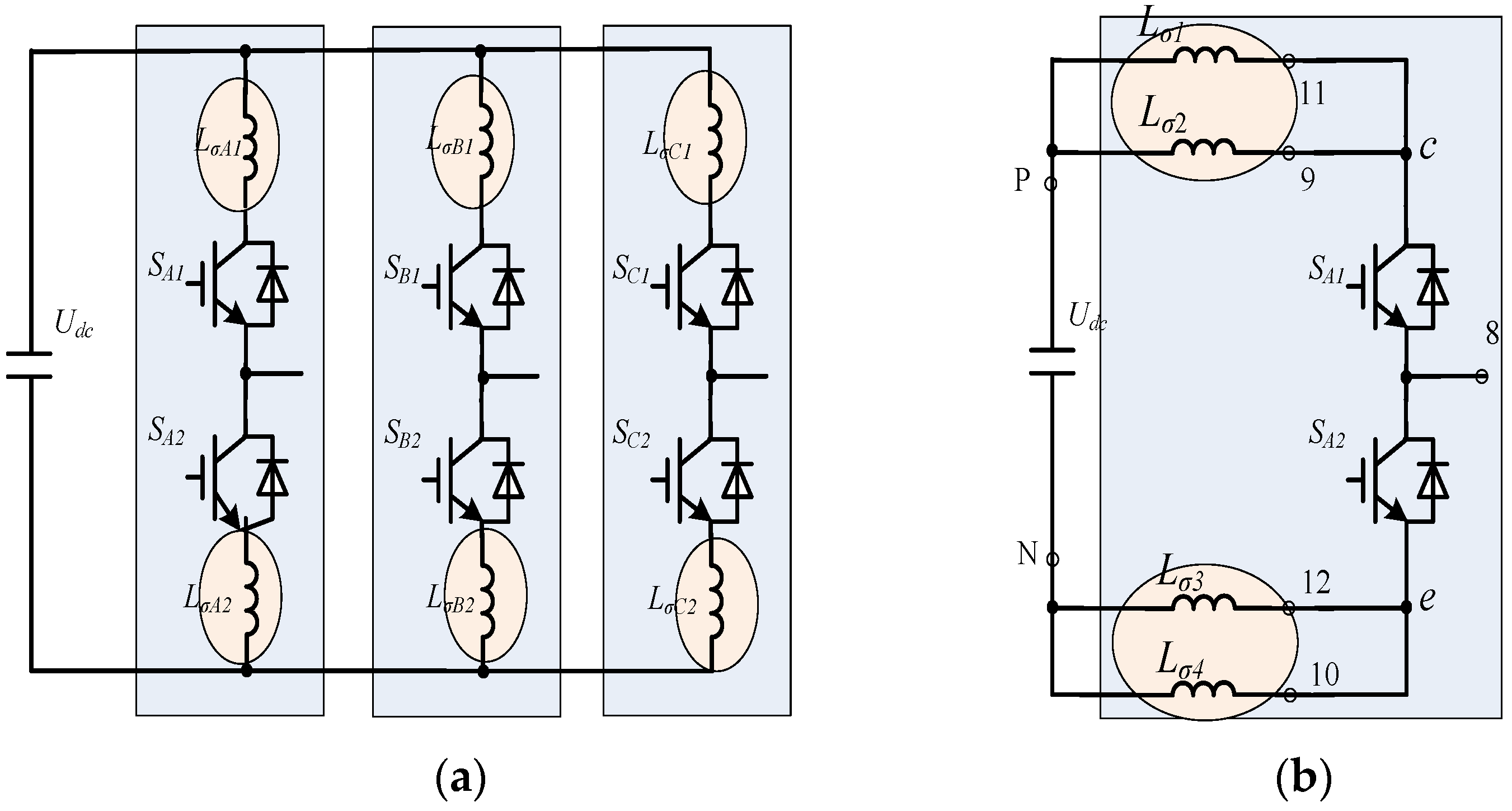
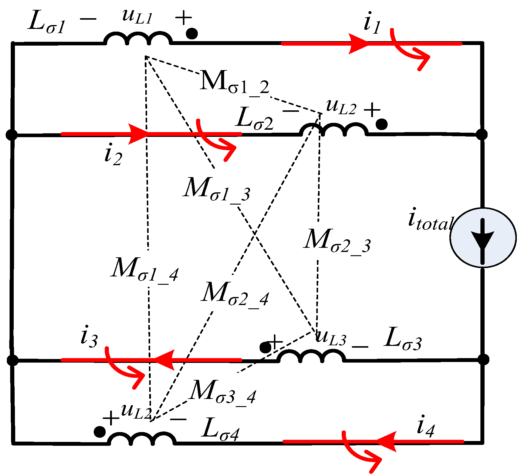
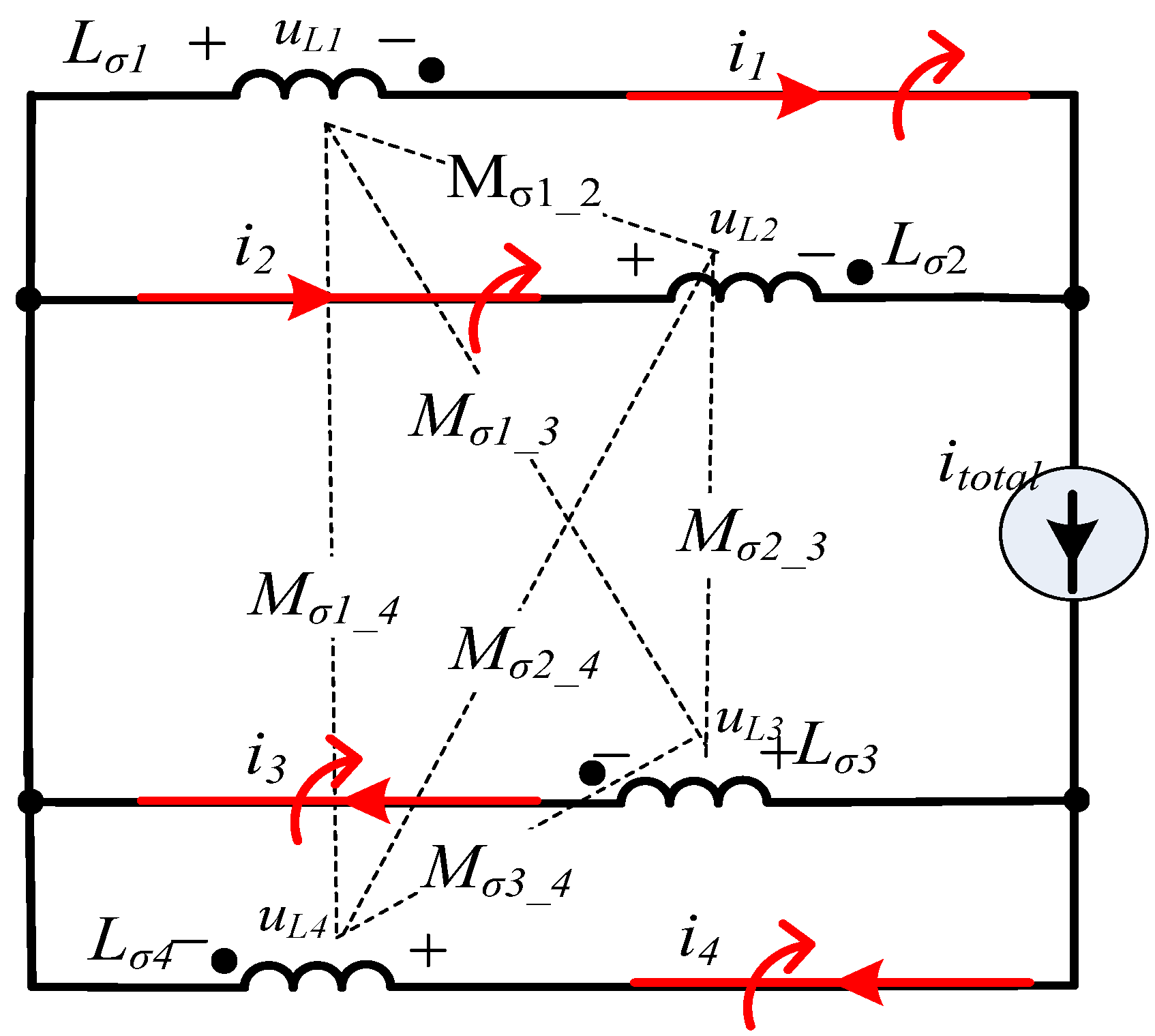
This paper focuses on the stray inductance of parallel branches of the bus-bar, without the consideration of the stray inductance in the capacitor and IGBT module. The simplified stray inductance model of the three phase inverter is shown in Figure 4a. The detailed stray inductance model with the consideration of the asymmetrical parallel branch of every phase on the bus-bar is shown in Figure 4b. Lσ1 and Lσ2 represent stray inductance from positive DC bus terminal P to terminals 9 and 11 respectively. Lσ3 and Lσ4 represent the stray inductance from negative DC bus terminal N to terminals 12 and 10 respectively.
3. Transient Analysis and Modeling of Asymmetrical Branches
3.1. Transient Analysis
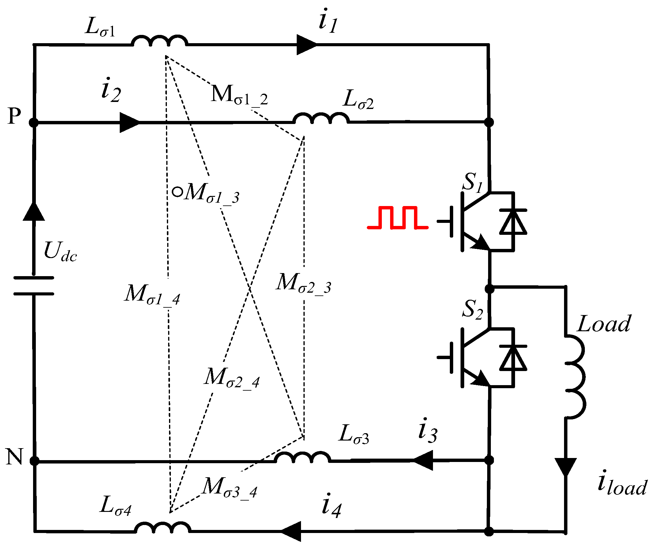
There are eight switch states for a three-phase inverter and only one power device is permitted to change state at any time under normal operation conditions. The double pulse test is used to test the IGBT over-voltage and stray inductance of the bus-bar, meanwhile, every phase shares the same testing principle, and this paper defines phase B as the example. Figure 5 is the basic principle of the test circuit. The i1, i2, i3, and i4 represent the current in the branches of Lσ1, Lσ2, Lσ3, and Lσ4. Furthermore, taking Proximity Effect into consideration, coupled inductance exists among the four current branches.
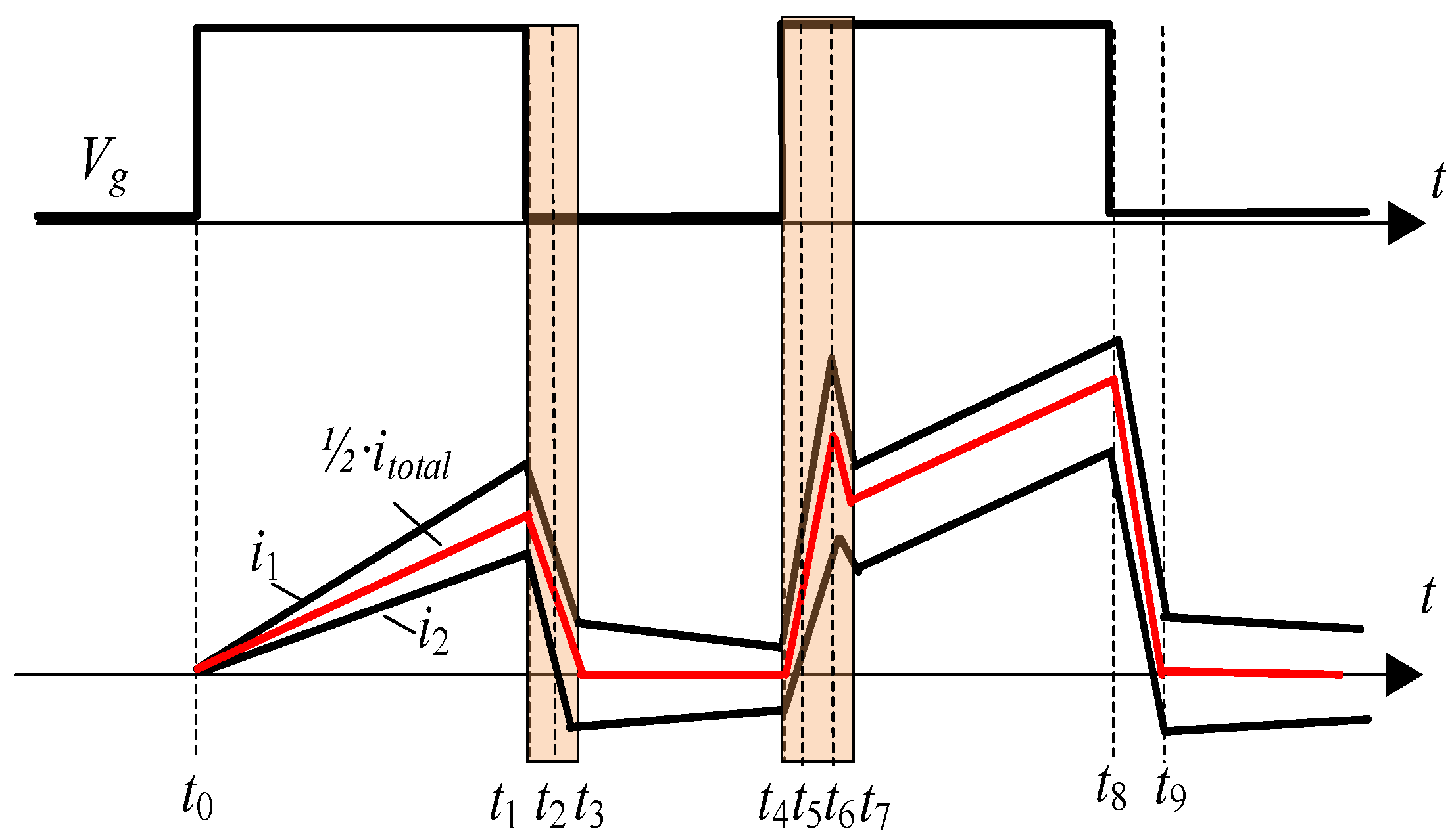
The transient analysis is based on the two branches of Lσ1 and Lσ2, and the waveforms of the double pulses test is depicted in Figure 6. The time intervals of t0–t1, t3–t4, and t7–t8 represent steady-state of conducting and blocking. This paper focuses on the transient process of turn-on and turn-off which refers to the time interval of t1–t3 and t4–t7, and the current in t8–t9 shares the same characteristics with current in the t1–t3 time interval.
3.1.1. Turn-Off Transient
At t1, S1 receives the turn-off signal and the bus-bar can be equivalent to the circuit depicted in Figure 7, in which itotal represents the turn-off current. According to Kirchhoff’s Current Law, the branch current satisfies i1 + i2 = i3 + i4 = itotal, meanwhile, the voltage in stray inductance of each branch satisfies uL1 = uL2 and uL3 = uL4.
The turn-off process of an IGBT can be regarded as the stray inductance energy releasing process, so the following analysis is based on magnetic field energy stored in the stray inductance. At t1, the energy stored in branches Lσ1 and Lσ2 are given as
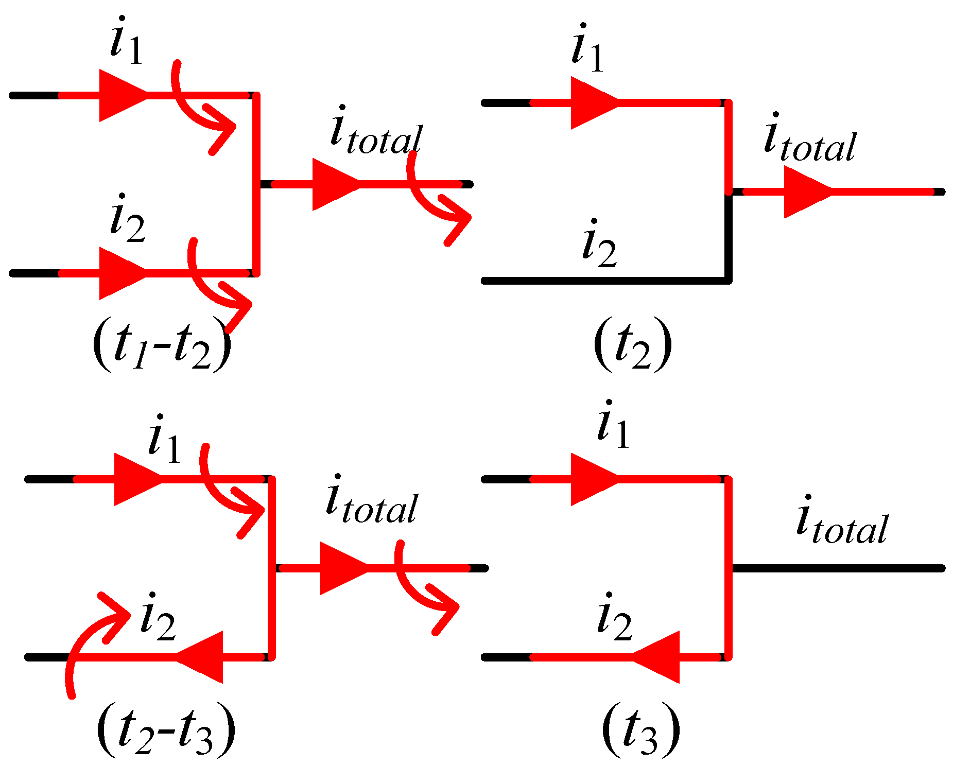
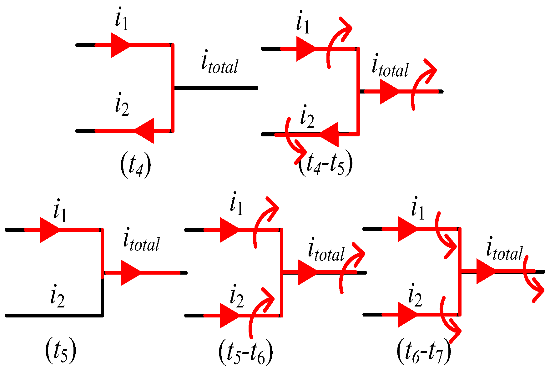
WLσ1(t1) and WLσ2(t1) are determined by the current and inductance in the two branches at t1, meanwhile, S1 starts to turn off and itotal starts to decrease. Hence, the energy stored in Lσ1 and Lσ2 begins to release, moreover, the speed of releasing is determined by the stray inductance in the two branches and the speed of turn-off. If the energy stored in Lσ1 and Lσ2 is released completely at t3 simultaneously, that means WLσ1(t3) = 0 and WLσ2(t3) = 0, and the current direction in the two branches depicted in Figure 7 does not change from t1 to t3. If the energy stored in Lσ1 and Lσ2 does not release completely at t3 simultaneously, that means WLσ1(t2) ≠ 0 or WLσ2(t2) ≠ 0 and one of the two branches must be released completely prior to the other. This study supposes the energy stored in Lσ2 releases completely at t2, namely i2(t2) = 0. From t1 to t2, the current i1 and i2 decrease gradually shown in Figure 8 (t1–t2) but the current direction does not change. At t2, i1(t2) = itotal(t2) and Lσ1 can be equivalent to a power source, and the direction of potential is shown in Figure 7, so the branch of Lσ2 provides the path of energy release for Lσ1 that means the current i2 changes direction from t2 and increases at the same slope as i1 shown in Figure 8 (t2–t3), but they share the contrary direction. At t3, the current i1 and i2 are equal in magnitude and opposite in direction and itotal = 0, moreover, neglecting the influence of tail current, the IGBT is closed completely. Due to the asymmetrical stray inductance in branches Lσ1 and Lσ2, a loop current is caused after turning off the IGBT.
At the turn-off transient, due to uL1 = uL2, the variation ratio of i1 and i2 can be calculated by
3.1.2. Turn-On Transient
At t4, S1 receives the open signal, due to the reverse recovery characteristic of the freewheeling diode inside S2, and S2 is equivalent to a short-circuit. The equivalent circuit is depicted in Figure 9.
i1(t4) and i2(t4) are mainly associated with the commutation between Lσ1 and Lσ2 during t3–t4. At t4, if the energy stored in Lσ1 and Lσ2 is released completely, that means WLσ1(t4) = 0 and WLσ2(t4) = 0, also i1(t4) = 0 and i2(t4) = 0. Starting from t4, i1 and i2 increase rapidly from zero to the peak of reverse recovery current, the rising slope is related to the stray inductance in the branch, and the magnitude and direction of current is shown in Figure 9. If the energy stored in Lσ1 and Lσ2 does not release completely during t3–t4, that means some loop current exists and i1(t4) = − i2(t4), as depicted in Figure 10 (t4). Starting from t4, due to the external voltage, i1 increases rapidly and i2 decreases to zero quickly, as depicted in Figure 10 (t4–t5), until i1(t5) = itotal(t5), as depicted in Figure 10 (t5). Then, starting from t5, i1 and i2 keep the same direction and rise to maximum value at the same time. During the period of t6–t7, the reverse recovery current is at the vanishing stage and is equivalent to the load current iload. Similar to the turning-off process, i1 and i2 may change direction, but the differential of the two currents can also be described by Formula (2).
3.2. Model of Stray Inductance
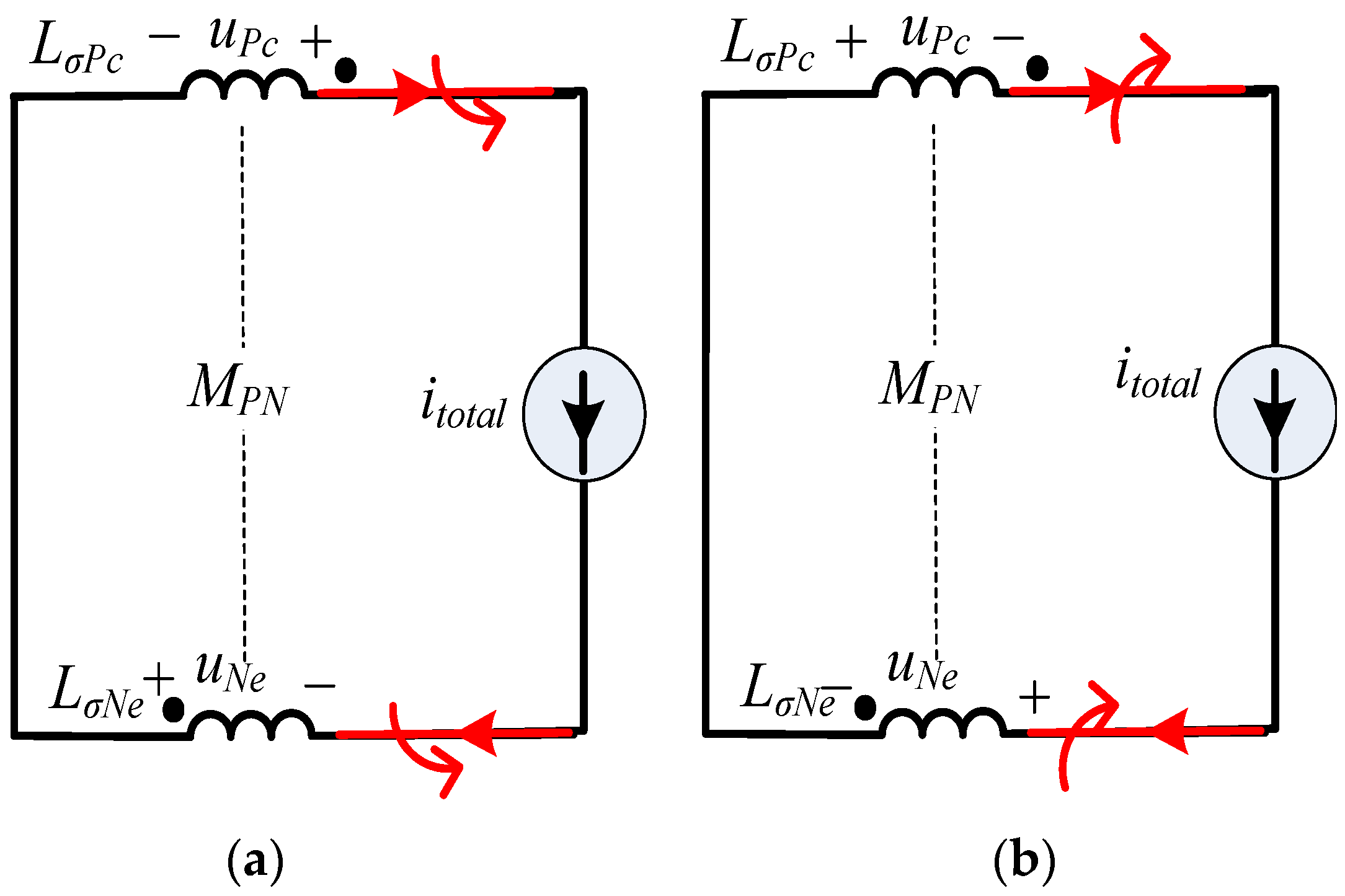
Based on the above analysis, although the direction of current changes at the turn-on transient or the turn-off transient, the position of the bus-bar does not change, and the dotted terminals of the branch equivalent inductance remains the same. Ultimately, the over-voltage caused by mutual inductance also stays the same.
The partial stray inductance model for Lσ1, Lσ2, Lσ3, and Lσ4 is as follows:
The uL1, uL2, uL3, and uL4 represent induced voltage of stray inductance Lσ1, Lσ2, Lσ3, and Lσ4, respectively, at the switching transient. The Lsσ1, Lsσ2, Lsσ3, and Lsσ4 represent self-inductance in branches Lσ1, Lσ2, Lσ3, and Lσ4. Meanwhile the M12(M21), M13(M31), M14(M41), M23(M32), M24(M42), and M34(M43) represent the mutual-inductance for each branch.
While measuring the bus-bar stray inductance, only the transient voltage and current of the bus-bar are available, so the measured values are all of equivalent stray inductance, and the mathematical model is as follows.
According to Equation (3) and (4), the bus-bar equivalent stray inductance is expressed as:
For Equation (5), the differential is difficult to obtain from measurement at the turn-off transient. Because of the excellent linearity at the turn-on transient, the differential can be replaced by difference.
The induced voltage in the switching transient of the stray inductance LσPc and LσNe meets:
where, uPc = uL1 = uL2, uNe = uL3 = uL4. LsσPc and LsσNe represent the self inductance and mutual inductance of LσPc and (between) LσNe. The current matrices meet:
Based on Equations (7) and (8), the simplified inductance matrix meets as:
where:
4. Measuring Method for Partial Stray Inductance
4.1. Basic Principle
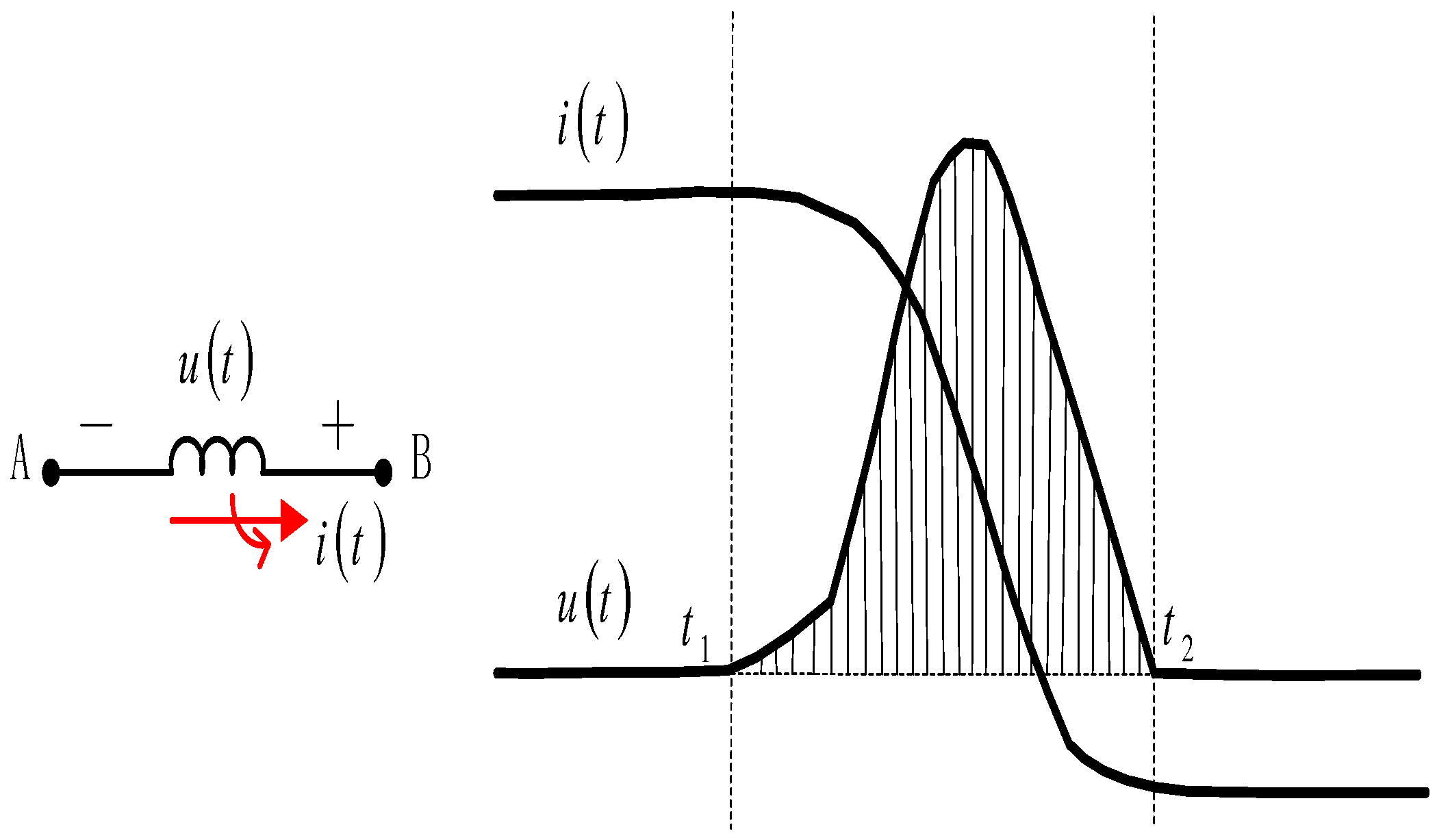
The measuring principle for partial stray inductance is based on the inductance voltage integral method [20]. Under high frequency, the stray inductance is determined by the inductance outside the conductor, tending to be constant. The voltage and current waveform of the stray inductance at the turn-off process of an IGBT is shown in Figure 12.
Furthermore, the voltage on stray inductance depends on the changing rate of current, expressed by following equation:
By the calculation of the definite integral for Equation (11), the bus-bar partial stray inductance is obtained and t1–t2 represents the time of the turn-on transient or turn-off transient.
4.2. Measurement Error Analysis
Based on Equation (12), the measured value of partial stray inductance is determined by the integral value of voltage during the period of t1–t2 and the values of i(t2) and i(t1). So, the precise partial stray inductance can be obtained once the integral value of the voltage and the two transient current values are available.
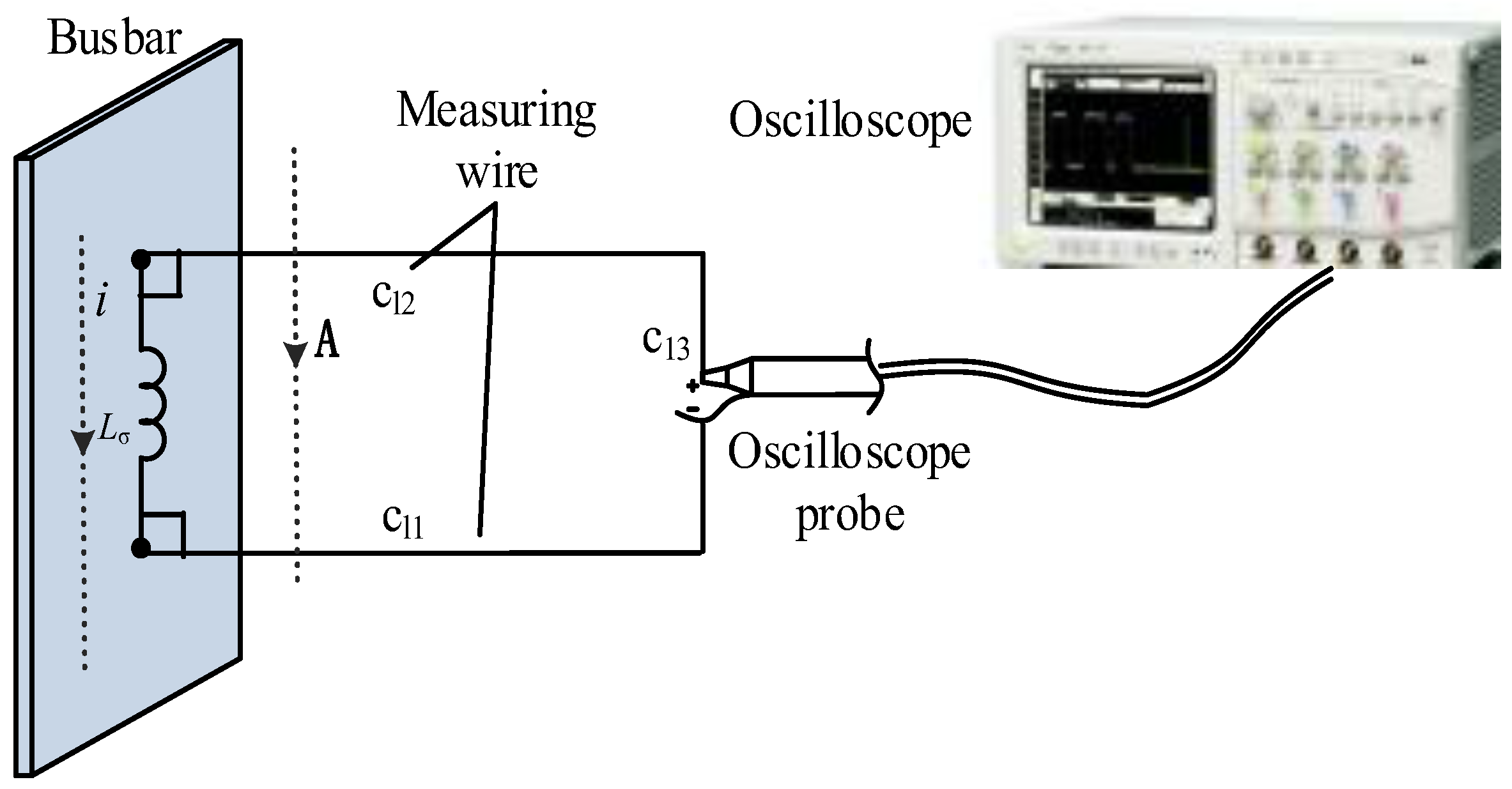
The measurement diagram of stray inductance is shown in Figure 13. Because the bus-bar partial stray inductance is very small, the voltage on the stray inductance at the switching transient is also very small, so a passive probe is needed to raise the bandwidth and precision of the voltage measurement. The probe of the oscilloscope is a high impedance circuit, vulnerable to the interference of an external magnetic field, and the interference source is mainly the voltage on the measuring lead-wire caused by the spatial transient magnetic field.
The measuring wire is divided into cl1, cl2, and cl3, shown in Figure 13. According to the theory of partial inductance, the induced voltage on the measuring lead-wire caused by the spatial transient magnetic field can be expressed by:
A represents the magnetic vector potential caused by the bus-bar current and the magnitude and direction is decided by the Biot–Savart law [14]
J represents the current density vector. Based on Formula (14), A shares the same direction with the current and is inversely proportional to the distance from the bus-bar in magnitude. So, the measuring precision can be raised, guaranteeing the lead-wire cl1 and cl2 are perpendicular to the bus-bar, and cl3 is very far from the bus-bar. If the distance between cl3 and bus-bar exceeds a certain value, the measuring voltage remains constant, which stands for the measured value with high precision.
5. Simulation and Experimental Results
5.1. Parameter Extraction
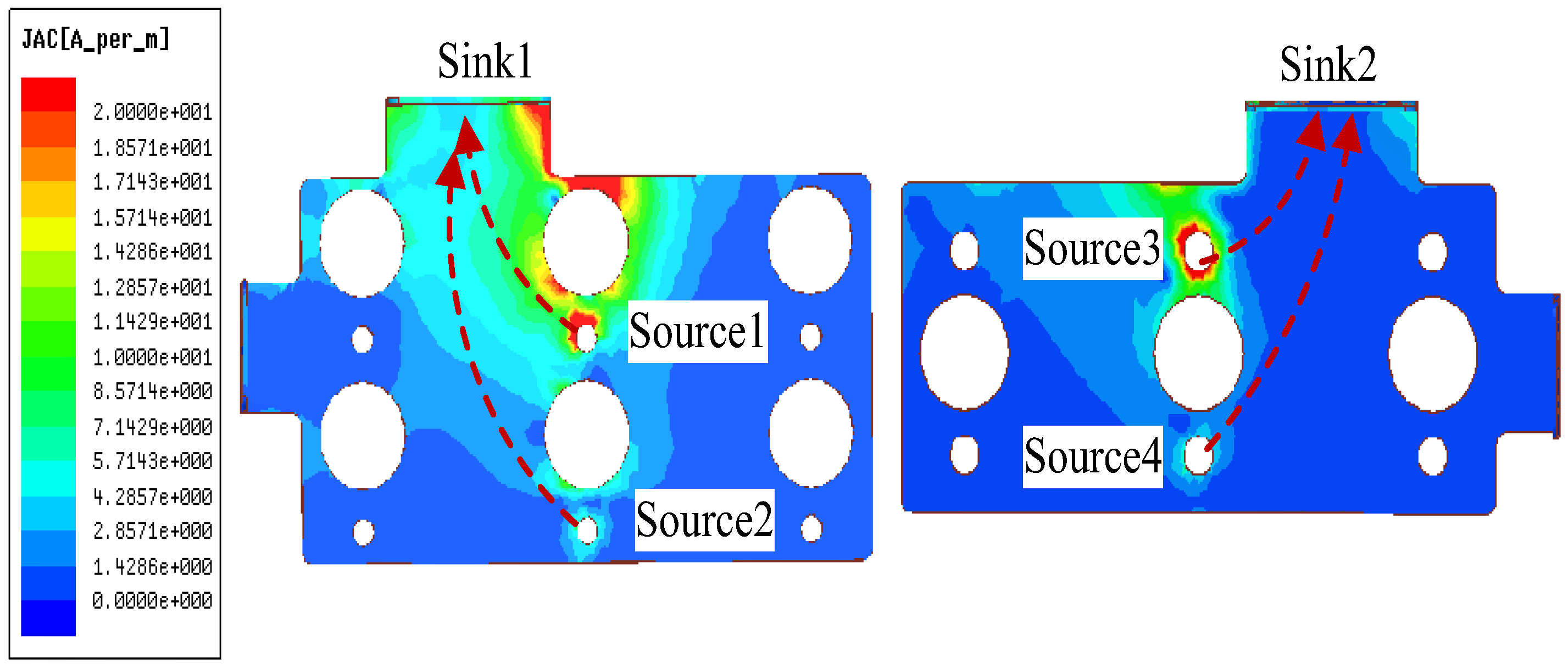
Ansys Q3D software was used to extract the partial stray inductance of the laminated bus-bar model in this study to verify the measured values of partial stray inductance. For extraction of the partial stray inductance, a current source and sink must be set up. For a certain conductor, only one current sink is allowed, but multiple current sources are permitted in the Q3D software. Taking the proximity effect of the bus-bar into consideration, excitation is demanded for both a positive bus-bar and a negative bus-bar to simulate the model. The positive bus-bar terminals 9 and 11 are set as Source2 and Source1 and the capacitor anode is set as Sink1. Similarly, the negative bus-bar terminals 10 and 12 are set as Source4 and Source3 and the capacitor cathode is set as Sink2. The excitation source settings and simulated current density of the bus-bar is shown in Figure 14. Because the excitation has the opposite direction of the actual current, the simulated mutual inductance in the branches of the positive bus-bar and negative bus-bar must be negative. The self inductance and mutual inductance of the asymmetrical parallel branches are described in Table 1.
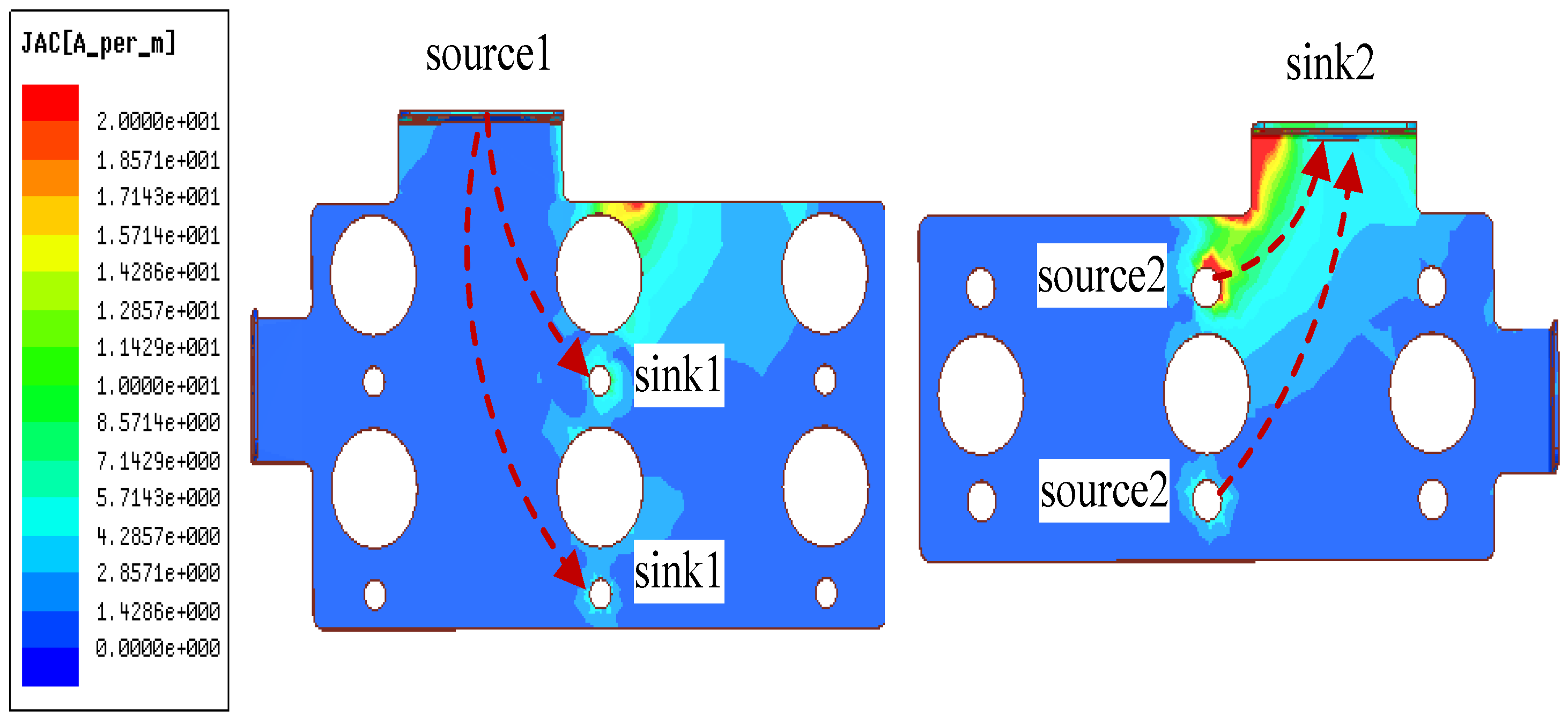
In order to verify the accuracy of the simplified model, the stray inductance LσPc and LσNe should be extracted based on simulation. The capacitor anode is set as Source1, and the positive bus-bar terminals 9 and 11 are set as Sink1. Similarly, the negative bus-bar terminals 10 and 12 are set as Source2 and the capacitor cathode is set as Sink2. The simplified model excitation source settings and current density of the bus-bar are shown in Figure 15. The simulated self inductance and mutual inductance of the simplified branch shown in Figure 10 are described in Table 2.
The simplified inductance matrix calculated based on Equation (9) is shown in Table 3. Calculation results are compared with the simulated results in Table 2. They have only 1 nH difference. That means the calculated values can match the simulated values very well, and the simplified method is accurate.
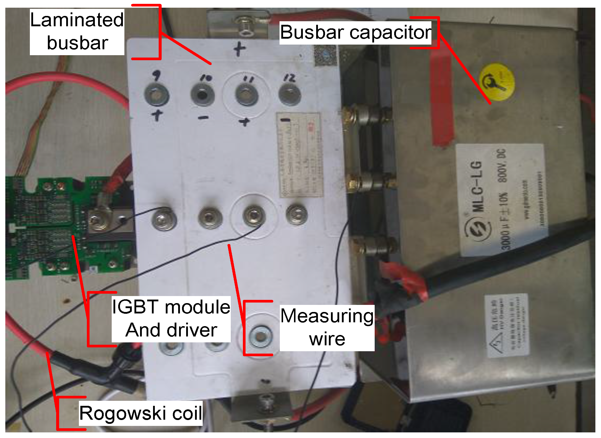
5.2. Experimental Measurement
In order to measure the branch stray inductance, the inverter testing platform is constructed as shown in Figure 16. The measuring equipment and power device are shown in Table 4. It must be noted that the oscilloscope must have the function of multi-channel digital integral that can measure the stray inductance of the two parallel branches under the same conditions. The experimental test is classified as the direct measuring method and the indirect measuring method. For the indirect measuring method, a Rogowski coil is adopted to measure the transient current variation ratio in the four branches. Meanwhile, using the simulation value of the stray inductance and Equation (6), the equivalent stray inductance can be obtained. The direct measuring method can be realized by the method proposed by the paper.
5.3. Indirect Measurement
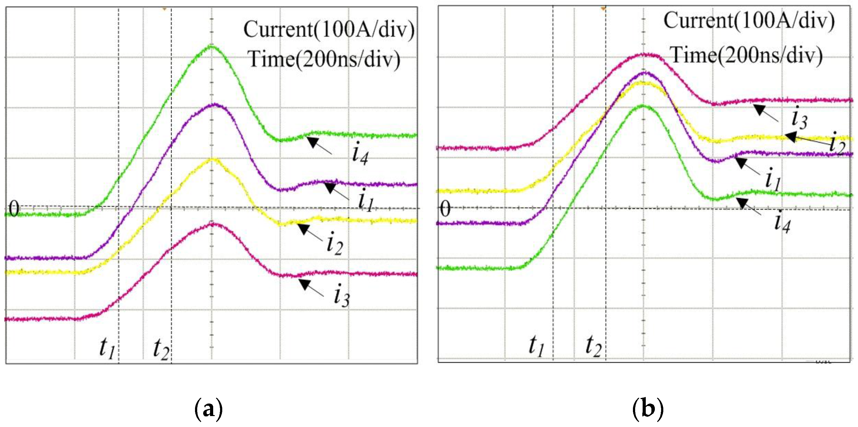
Due to the excellent linearity of the transient current of the IGBT module at the turn-on transient, the indirect measurement takes the turn-on transient as an example. In order to verify the consistency of the transient current’s change rate under different testing conditions, a double pulse test is applied on S1 and S2. At first, according to the phase leg testing circuit shown in Figure 5, S1 is tested with a double pulse, then, upon switching the position of the load, S2 is tested also with the double pulse. The transient current i1, i2, i3, and i4 shown in Figure 17a,b, corresponding to the second turn-on of lower module S2 and upper module S1, and their main difference is the current magnitude and direction before turn on. The variation in the transient current is basically consistent after turning on. Choosing Δt = t1 − t2 = 100 ns and recording the difference of the two moments, because the oscilloscope has sampling error, tests are made many times for each testing method to compute the arithmetic mean value to raise measurement accuracy. Table 5 shows the average values for fifty repeat measurements of the upper IGBT module and lower IGBT module at the turn-on transient.
5.4. Direct Measurement
The direct measurement is based on the inductance voltage integral method regardless of the current linearity. Therefore, it can be realized at the turn-on transient or the turn-off transient. The voltage sampling error is very small, because the voltage is based on digital integration function. However, the current is sampled at t1 and t2 moments, so the current sampling error is relatively large. In order to raise measurement precision, tests are made many times at both the turn-on transient and the turn-off transient.
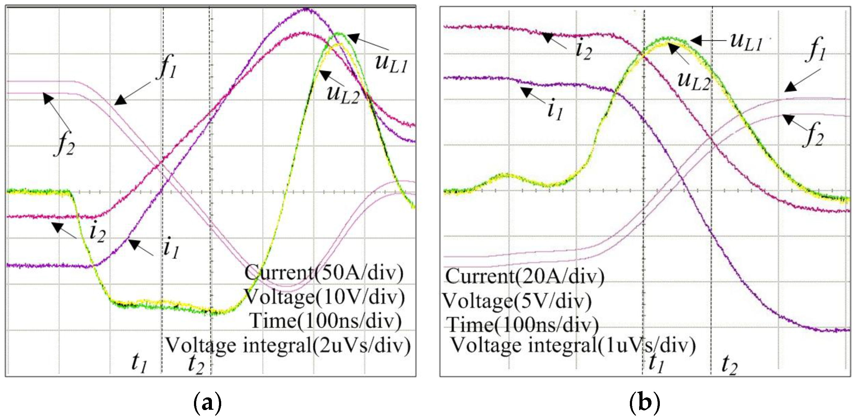
Due to the limited channel amounts of the oscilloscope, Lσ1 and Lσ2 are extracted firstly, as shown in Figure 18a,b, in which the i1 and i2 are the current waveforms at the switching transient in branches Lσ1 and Lσ2. Also, uL1 and uL2 are the voltage waveforms at the switching transients on branches Lσ1 and Lσ2. It is observed that the voltage variation is basically consistent at the switching transient. f1 and f2 represent the time integral of uL1 and uL2 and the integral time is 100 ns.
The partial stray inductance for Lσ1 and Lσ2, based on the turn-on transient and the turn-off transient, are listed in Table 7. According to the same testing conditions, Lσ3 and Lσ4 are measured, as shown in Table 7. It is observed that the measurement difference is within 3 nH at both the turn-on transient and the turn-off transient, so the turn-on transient and the turn-off transient are valid for the extraction of partial stray inductance.
The stray inductance mean values obtained from indirect measurement and direct measurement are shown in Table 8. The measurement difference is within 5 nH so the consistency is very high.
LσPc and LσNe are measured based on the proposed direct measuring method. As shown in Table 9, the measurement values are almost the same as the simulation values and the calculated values. So, simulation, calculation, and measurement can validate each other, which can further prove the accuracy of the modeling and measuring method.
6. Conclusions
In this paper, the laminated bus-bar of a three-phase inverter in an electric vehicle with asymmetric branching is investigated. For the first time, the imbalanced transient current on the bus-bar is deeply analyzed from the view of stray inductance energy storage and release. The partial self-inductance and mutual-inductance model of the asymmetrical parallel branches on the bus-bar is built and the technique to reduce the equivalent inductance circuit models is developed based on matrix calculation. Furthermore, a high-precision partial inductance measuring method considering spatial electromagnetic transient field is proposed. At last, both the simulation values based on Q3D and the calculation values based on matrix calculation are verified using the proposed direct and indirect measurement methods.
For future work, frequency-domain simulations will be conducted to investigate the effects of the asymmetrical stray inductance on the inverter’s EMI performance. This will provide insight for effective component layout inside the enclosure of EV inverters.
Acknowledgments
The project is supported by the National Key Research and Development Program of China (2016YFC0600906).
Author Contributions
Fengyou He and Chengfei Geng conceived and designed the experiments. Chengfei Geng designed and performed the simulations. Jingwei Zhang performed the experiments. Chengfei Geng and Hongsheng Hu wrote the paper.
Conflicts of Interest
The authors declare no conflict of interest.
References
- Un-Noor, F.; Padmanaban, S.; Mihet-Popa, L.; Mollah, M.N.; Hossain, E. A Comprehensive Study of Key Electric Vehicle (EV) Components, Technologies, Challenges, Impacts, and Future Direction of Development. Energies 2017, 10, 1217. [Google Scholar] [CrossRef]
- Bucher, A.; Schmidt, R.; Werner, R.; Leipenat, M.; Hasenohr, C.; Werner, T.; Schmitz, S.; Heitmann, A. Design of a Full SiC Voltage Source Inverter for Electric Vehicle Applications. In Proceedings of the 18th European Conference on Power Electronics and Applications (EPE’16 ECCE Europe), Karlsruhe, Germany, 5–9 September 2016; pp. 1–10. [Google Scholar]
- Liu, J.; Sun, W.; Su, W.; Tai, X.; Wen, X. Inverter Output Power Density Increasing Technologies for EV/HEV Applications. In Proceedings of the 19th International Conference on Electrical Machines and Systems (ICEMS), Chiba, Japan, 13–16 November 2016; pp. 1–4. [Google Scholar]
- Mühlfeld, O.; Paulsen, L.; Olesen, K.; Ströbel-Maier, H. Automotive Traction Inverter for Highest Power Density. In Proceedings of the International Exhibition and Conference for Power Electronics, Intelligent Motion, Renewable Energy and Energy Management, Nuremberg, Germany, 19–20 May 2015; pp. 871–878. [Google Scholar]
- Caponet, C.; Profumo, D.; Doncker, W. Low stray inductance bus bar design and construction for good EMC performance in power electronic circuit. IEEE Trans. Power Electron. 2002, 17, 225–231. [Google Scholar] [CrossRef]
- Chen, C.; Pei, X.; Chen, Y.; Kang, Y. Investigation, Evaluation, and Optimization of Stray Inductance in Laminated Busbar. IEEE Trans. Power Electron. 2014, 29, 3679–3693. [Google Scholar] [CrossRef]
- Wang, J.; Yang, B.-J.; Xu, Z.-X.; Deng, Y.; Zhao, R.-X.; He, X.-N. Configuration of Low Inductive Laminated Bus Bar in 750 kVA NPC Three-level Universal Converter Module of High Power Density. Proc. CSEE 2010, 30, 47–54. [Google Scholar]
- Callegaro, A.D.; Guo, J.; Eull, M.; Gibson, J.; Preindl, M.; Bilgin, B. Bus Bar Design for High-Power Inverters. IEEE Trans. Power Electron. 2017. [Google Scholar] [CrossRef]
- Xuesong, W.; Zhengming, Z.; Liqiang, Y. Conducted EMI Reduction in IGBT Based Converters. In Proceedings of the Asia-Pacific International Conference on Electromagnetic Compatibility (APEC), Beijing, China, 12–16 April 2010. [Google Scholar]
- Khan, M.; Magne, P.; Bilgin, B.; Wirasingha, S.; Emadi, A. Laminated Busbar Design Criteria in Power Converters for Electrified Powertrain Applications. In Proceedings of the 2014 IEEE Transportation Electrification Conference and Expo (ITEC), Dearborn, MI, USA, 15–18 June 2014; pp. 1–6. [Google Scholar]
- Dong, Y.F.; Luo, H.Z.; Yang, H.Y.; He, Y.M.; Li, W.H.; He, X.G. Engineering Design for Structure and Bus Bar of 1.2MV·A Hybrid Clamped Five-Level Converter Module. Trans. China Electrotech. Soc. 2016, 31, 11–18. [Google Scholar]
- Schanen, J.L.; Clavel, E.; Roudet, J. Modeling of Low Inductive Bus bar Connection. IEEE Ind. Appl. Mag. 1996, 2, 39–43. [Google Scholar] [CrossRef]
- Ruehli, A.E. Inductance Calculations in a Complex Integrated Circuit Environment. IBM J. Res. Dev. 1972, 16, 470–481. [Google Scholar] [CrossRef]
- Paul, C.R. Inductance, Loop and Partial; Willey & Sons: New York, NY, USA, 2010; pp. 246–254. [Google Scholar]
- Bryant, A.T.; Vadlapati, K.K.; Starkey, J.P.; Goldney, A.P.; Kandi-lidis, S.Y.; Hinchley, D.A. Current distribution in high power laminated busbars. In Proceedings of the 14th European Conference on Power Electronics and Application, Birmingham, UK, 30 August–1 September 2011; pp. 1–10. [Google Scholar]
- Pasterczyk, R.J.; Martin, C.; Guichon, J.-M.; Schanen, J.-L. Planar Busbar Optimization Regarding Current Sharing and Stray Inductance Minimization. In Proceedings of the European Conference on Power electronics and applications, Dresden, Germany, 11–14 September 2005; pp. 1–9. [Google Scholar]
- Zhang, N.; Wang, S.; Zhao, H. Develop Parasitic Inductance Model for the Planar Busbar of an IGBT H Bridge in a Power Inverter. IEEE Trans. Power Electron. 2015, 30, 6924–6933. [Google Scholar] [CrossRef]
- Eupec marketing department; European Power Semiconductor; Electronics Company. Measurement of the Circuit Stray Inductance Lσ; Application Note; European Power Semiconductor and Electronics Company: Warstein, Germany, 1999. [Google Scholar]
- Zhu, H.; Hefner, R.; Allen, R.; Lai, J.-S. Characterization of power electronics system interconnect parasitics using time domain reflectometry. IEEE Trans. Power Electron. 1999, 14, 622–628. [Google Scholar]
- Feng, G.; Yuan, L.; Zhao, Z.; Zhao, J.; Lu, T. A Novel Stray Inductance Extraction Method for Bus Bars Based on Turn-on/off Transient Process. Proc. CSEE 2014, 34, 6442–6449. [Google Scholar]
- Wen, H.; Liu, J.; Zhang, X.; Wen, X. Electric Vehicle Drive Inverters Simulation Considering Parasitic Parameters. In Proceedings of the 13th International Power Electronics and Motion Control Conference, Poznan, Poland, 1–3 September 2008; pp. 417–421. [Google Scholar]
Figure 1.
The structure of the EV motor driver system (MDS). (a) External structure; (b) Internal structure.
Figure 1.
The structure of the EV motor driver system (MDS). (a) External structure; (b) Internal structure.

Figure 2.
The structure and circuit principle of the IGBT module.

Figure 3.
Structure of the bus-bar.

Figure 4.
Equivalent circuit of every phase leg. (a) Simplified circuit; (b) Detailed circuit.

Figure 5.
The test circuit of every phase leg.

Figure 6.
The waveforms of the double pulse test.

Figure 7.
The equivalent circuit of the turn-off transient.

Figure 8.
The current direction of parallel branches at the turn-off transient.

Figure 9.
The equivalent circuit of the turn-on transient.

Figure 10.
The current direction of parallel branches at the turn-on transient.

Figure 11.
The simplified equivalent circuit in the switching transient. (a) Turn off transient; (b) turn on transient.
Figure 11.
The simplified equivalent circuit in the switching transient. (a) Turn off transient; (b) turn on transient.

Figure 12.
The current, voltage waveform of inductance at the turn-off transient.

Figure 13.
The measuring method of partial stray inductance.

Figure 14.
The excitation source settings and simulated current density of the bus-bar.

Figure 15.
The simplified model excitation source settings and current density of the bus-bar.

Figure 16.
The experimental platform.

Figure 17.
The current waveform at the turn-on transient. (a) Second turning-on of S2; (b) Second turning-on of S1.
Figure 17.
The current waveform at the turn-on transient. (a) Second turning-on of S2; (b) Second turning-on of S1.

Figure 18.
The test waveform at the turn-off transient. (a) Turn-on transient; (b) Turn-off transient.
Figure 18.
The test waveform at the turn-off transient. (a) Turn-on transient; (b) Turn-off transient.


Table 1.
Simulated partial stray inductance matrix.
| nH | Lσ1 | Lσ2 | Lσ3 | Lσ4 |
|---|---|---|---|---|
| Lσ1 | 22.72 | 23.95 | −1.56 | −7.56 |
| Lσ2 | 23.95 | 37.42 | −2.18 | −14.5 |
| Lσ3 | −1.56 | −2.18 | 17.18 | 17.48 |
| Lσ4 | −7.56 | −14.5 | 17.48 | 29.37 |
Table 2.
Simulated stray inductance matrix.
| nH | LσPc | LσNe |
|---|---|---|
| LσPc | 17.81 | −1.44 |
| LσNe | −1.44 | 16.46 |
Table 3.
Calculated stray inductance matrix.
| nH | LσPc | LσNe |
|---|---|---|
| LσPc | 19.14 | −1.51 |
| LσNe | −1.51 | 17.15 |
Table 4.
The experimental equipment.
| Equipment | Parameter |
|---|---|
| IGBT module | FF1400R12IP4 |
| IGBT driver | 2SP0320V2A0 |
| Rogowski coil | CWT30B |
| Voltage probe | Agilent-10073C |
| Oscilloscope | Agilent-MSO8064A |
| Inductive load | About 7uH |
Table 5.
Measured current values.
| Δi(A) | Δi1 | Δi2 | Δi3 | Δi4 |
|---|---|---|---|---|
| S1 | 104.57 | 76.71 | 66.36 | 108.46 |
| S2 | 106.25 | 75.21 | 70.35 | 110.36 |
| nH | Lσ1 | Lσ2 | Lσ3 | Lσ4 |
|---|---|---|---|---|
| Turn on transient of S1 | 31.45 | 47 | 40.68 | 28.11 |
| Turn on transient of S2 | 30.69 | 47.9 | 39.8 | 24 |
| Difference | 0.76 | 0.9 | 0.88 | 4.11 |
Table 7.
The measured values of Lσ1 and Lσ2.
| nH | Lσ1 | Lσ2 | Lσ3 | Lσ4 |
|---|---|---|---|---|
| Turn-on transient | 30.56 | 45.6 | 39.56 | 26.6 |
| Turn-off transient | 31.37 | 42.77 | 41.37 | 27.57 |
| Difference | 0.81 | 2.83 | 1.81 | 0.97 |
Table 8.
Comparison of stray inductance based on indirect and direct measurements.
| nH | Lσ1 | Lσ2 | Lσ3 | Lσ4 |
|---|---|---|---|---|
| Indirect measurement | 31.56 | 47.4 | 40.24 | 26.01 |
| Direct measurement | 30.9 | 44.19 | 40.46 | 27.1 |
| Difference | 0.66 | 3.21 | 0.22 | 1.01 |
Table 9.
Comparison of stray inductance based on simulation, calculation, and measurement.
| Method | LσPc | LσNe |
|---|---|---|
| simulation | 16.37 | 15.02 |
| calculation | 17.6 | 15.6 |
| measurement | 17.2 | 16.1 |
© 2017 by the authors. Licensee MDPI, Basel, Switzerland. This article is an open access article distributed under the terms and conditions of the Creative Commons Attribution (CC BY) license (http://creativecommons.org/licenses/by/4.0/).
Share and Cite
MDPI and ACS Style
Geng, C.; He, F.; Zhang, J.; Hu, H. Partial Stray Inductance Modeling and Measuring of Asymmetrical Parallel Branches on the Bus-Bar of Electric Vehicles. Energies 2017, 10, 1519. https://doi.org/10.3390/en10101519
AMA Style
Geng C, He F, Zhang J, Hu H. Partial Stray Inductance Modeling and Measuring of Asymmetrical Parallel Branches on the Bus-Bar of Electric Vehicles. Energies. 2017; 10(10):1519. https://doi.org/10.3390/en10101519
Chicago/Turabian StyleGeng, Chengfei, Fengyou He, Jingwei Zhang, and Hongsheng Hu. 2017. "Partial Stray Inductance Modeling and Measuring of Asymmetrical Parallel Branches on the Bus-Bar of Electric Vehicles" Energies 10, no. 10: 1519. https://doi.org/10.3390/en10101519
Note that from the first issue of 2016, this journal uses article numbers instead of page numbers. See further details here.