
A Novel High Controllable Voltage Gain Push-Pull Topology for Wireless Power Transfer System


School of Automation, Chongqing University, 174 Shazheng Street, Shapingba District, Chongqing 400030, China
*
Author to whom correspondence should be addressed.
Energies 2017, 10(4), 474; https://doi.org/10.3390/en10040474
Submission received: 2 February 2017
/
Revised: 27 March 2017
/
Accepted: 29 March 2017
/
Published: 1 April 2017
(This article belongs to the Section F: Electrical Engineering)
Abstract
:Wireless Power Transfer (WPT) is commonly used to transmit power from a transmitting coil to various movable power devices. In the WPT system, due to a resonant tank inherent characteristic, the system cannot achieve a high output voltage gain. This paper proposes a novel current-fed push–pull circuit to realize high output voltage gain by adding a bi-directional switch between the resonant network and inverter. To obtain a high voltage gain, this paper proposes energy storage and energy injection mode to realize an energy boost function. A duty cycle control method for mode switching is also proposed. The proposed method allows the converter to operate with a variable voltage gain over a wide range with high efficiency. Experimental validation shows that the system gain of a proposed circuit can achieve a variable gain from 2 to 7 of which the converter can be two times higher than the classical system with the same condition.

1. Introduction
The Wireless Power Transfer (WPT) system as a novel technology can realize power wireless transmission from power supply to electrical equipment with the aid of magnetic coupling. With its rapid development, more and more applications have appeared in electrical vehicles, biomedical implants and cell phone areas [1,2,3,4,5,6].
More and more applications in WPT technology require low DC voltage input and high voltage output. These applications include the Photovoltaic (PV) system, battery power supply system and Universal Serial Bus (USB) powered devices. However, it is not easy for the WPT system to obtain high voltage gain according to the following reasons—first, due to the WPT system being a weakly coupling system with very low coupling coefficient k (normally below 0.2) [7,8] and the coupling coefficient of transformer can almost reach 1. The second reason is the inherent characteristic of the resonant network. There are four fundamental resonant topologies SS, SP, PS, and PP (S and P denotes series and parallel topology, respectively). Series resonant network exhibits voltage source characteristics that cannot obtain a high voltage gain. The parallel resonant network exhibits current source characteristics that obtain high voltage gain on the light load condition. However, for heavy load conditions, it still cannot obtain high voltage gain. Furthermore, its reflecting impedance will bring relatively large frequency drift, which may cause a large reduction in output power [9,10]. For the same reason, composite resonant networks such as Inductor Capacitor Inductor (LCL), Inductor Capacitor Capacitor (LCC), and Capacitor Inductor Capacitor (CLC), which are combinations of the series and resonant topology, cannot reach high voltage gain. Reference [11] analyzes wireless charging circuit characteristics under hybrid compensation topology. The analysis results show that the output voltage gain is below three in hybrid compensation topology.
To achieve high output voltage gain, the classical method is implemented by placing an additional Boost converter at the primary or secondary side. However, the added Boost converter will increase the volume and weight of the whole system [12,13], and make the system complicated to control. There are few papers related with voltage gain improvement. Aiming at voltage gain optimization and control, Reference [14] proposes a uniform voltage gain control method. This method is implemented by control system operating frequency. However, the method only aims at improving the robustness against misalignment. Reference [15] proposes a detached magnetic core to improve the voltage gain method. The obtained voltage gain is 0.83. Reference [16] proposes an S/SP topology converter to obtain constant voltage gain. However, the voltage gain cannot be adjusted and will be very sensitive to frequency drift on the high gain condition.
In order to obtain a high and controllable output voltage gain WPT system, this paper proposes a novel current-fed push–pull converter at the primary side. A pair of Insulated Gate Bipolar Transistor (IGBT) switches, which act as a directional switch, is added in front of the resonant network to isolate the inverter and resonant network. An energy storage and injection switching mode is proposed to control the energy flowing into the resonant network. A switching duty cycle regulation method is also proposed to reach high voltage gain.
2. High Output Gain Push–Pull Circuit
The proposed high output gain push–pull circuit is shown in Figure 1. Compared with traditional push–pull circuits, the proposed circuit adds two additional switches S3 and S4 to form a bi-directional switch. At the primary side, a DC power supply is a series with an inductor to form a quasi-current source. A push–pull transformer including L1 and L2 is utilized to divide the DC current in half, so that the current flowing into the resonant tank is approximately a square waveform with half the magnitude of the input DC current. The primary side uses two main switches (S1 and S2) with a common ground and two auxiliary switches (S3 and S4) in series with a parallel-tuned resonant tank, which consists of a resonant capacitor CP, a resonant inductor LP and equivalent series resistance RP. The secondary side comprises a parallel resonant tank, which consists of a resonant inductor LS, equivalent series resistance RS, and a resonant capacitor CS. With the rectifier bridge (D1–D4) and Inductor Capacitor (LC) filter network, AC energy is transformed to DC output to the load R.
Aiming at voltage gain promotion, this paper proposes a resonant energy promotion method at the primary side. An energy storage mode is realized by shorting the DC inductor and phase-shifting transformer. An energy injection mode is realized by combining the storage energy and DC input energy together and outputting to the resonant tank. The switching between the energy storage and injection mode is implemented by auxiliary switch pair S3 and S4.
Figure 2 shows fundamental operation principles of the proposed method. The pulses and current waveforms of the proposed circuit switches are shown. VGE1 to VGE4 denotes the driving signals of switches S1 to S4, respectively. The current waveform of iL2 is similar to the current waveform of iL1, except for half-cycle delay. The function of anti-series switches (S3 and S4) is to control the connection between resonant tank and push–pull circuit. During one full switching cycle, the circuit operation can be divided into the following four modes and can be shown in Figure 3.
Mode I: t0–t1: In this mode, switches S2 and S4 are turned on; switches S1 and S3 are turned off. The operation of this mode is shown in Figure 3a. The energy stored in L1 is transfer into the resonant circuit by switch S4 and the reverse diode of S3; switch S2 is remaining conduction, so that the current flowing L2 is rising slowly and L2 is still working in the state of storage.
Mode II: t1–t2: In this mode, switches S1 and S2 are turned on and switches S3 and S4 are turned off. The operation of this mode is shown in Figure 3b. Switches S3 and S4 are turned off and the resonant circuit enters the state of free energy oscillation between LP and CP. Switches S1 and S2 are turned on and L1 and L2 are both working in the state of storage.
Mode III: t2–t3: In this mode, switches S1 and S3 are turned on; switches S2 and S4 are turned off. The operation of this mode is shown in Figure 3c. The energy stored in L2 is transferred into the resonant circuit by switch S3 and the reverse diode of S4 and the current flowing through L2 is decreasing; switch S1 is remaining conduction, so that the current flowing L1 is rising slowly and L1 is still working in the state of storage.
Mode IV: t3–t4: This mode is similarly with Mode II, switches S1 and S2 are turned on and switches S3 and S4 are turned off. The operation of this mode is shown in Figure 3d. Switches S3 and S4 are turned off and the resonant circuit enters the state of free energy oscillation between LP and CP. Switches S1 and S2 are turned on and L1 and L2 are both working in the state of storage.
3. Voltage Gain Analysis
Assuming that the resonant cycle of the circuit is T, and the switching duty cycle of S1 and S2 is D; correspondingly, the duty cycle of S3 and S4 is (1 − D). According to the volt–second balance of inductors L1 and L2, the average voltage across L1 and L2 is equal to zero during one switching cycle period. During the steady state, the current flows through L1 and L2 is equal so that the energy stored in inductors L1 and L2 is equal as well. Next, the paper will calculate the output gain based on the fact that the energy stored and released in inductor L1 is equal during one switching cycle.
In the steady state, the supply current is Id, and the current flowing through L1 or L2 is Id/2. Assuming the resonant network terminal voltage is UAB, thus the volt-second balance equation can be obtained as
Thus:
Note that duty cycle of switches S1 and S2 is no less than 0.5. It is because when the duty cycle is less than 0.5, switches S1 and S2 will enter the state of turning off at the same time; correspondingly, switches S3 and S4 will enter the state of turning on. It will result that the current of L1 and L2 drops sharply to zero and the current will become discontinuities. On the assumption, system equivalent circuit can be shown as Figure 4.
At the secondary side, according to the energy balance equation, the equivalent resistance Req of DC part including rectifier, filter and load at the secondary side is
The reflection impendence from the secondary to primary side can be expressed by
where ZS = (jωLS + RS) + Req/(jωCSReq + 1) is the input impendence of secondary resonant network. Its resonant angular frequency is ω = 2πf.
The input impendence of the push–pull network can be expressed as
The resonant current of the primary side IP can be expressed as
It is well known that the inductive voltage source of secondary side can be expressed as
On the resonant condition ω2LSCS = 1, the output voltage VO the load can be obtained as
Therefore, the voltage gain of the proposed circuit can be expressed as Equation (9)
Equation (9) shows that the output voltage can be controlled by duty cycle D, coupling coefficient k, switching frequency f and the equivalent resistance Req. However, frequency f and the load R usually are constant in the proposed circuit, thus the output voltage can be regulated by the duty cycle D of the push–pull switches S1 and S2.
Compared with traditional full-bridge circuit, its equivalent AC input UAB can be calculated by
In addition, the voltage gain of the full-bridge converter will be
As can be seen from Equations (9) and (11), we can draw a conclusion that the voltage gain of proposed topology can be at least two times than traditional full-bridge topology.
Compared with a traditional push–pull circuit, its equivalent AC input UAB can be calculated by
Furthermore, the voltage gain of the full-bridge converter will be
As can be seen from Equations (9) and (13), we can draw a conclusion that the voltage gain of proposed topology can achieve times the traditional push–pull topology.
4. System Performance Analysis
In order to analyze the performance of the proposed method, several performance analyses are carried out including load variation, coupling coefficient and comparison with a traditional WPT system.
4.1. Influence of Load (R) Variation on Voltage Gain and Efficiency
According to Equation (9), Figure 5 shows the voltage gain against switching duty cycle D with different load R, and the efficiency against load R when k = 0.2. The analysis results show
- (1)
- With the increase of switch duty cycle D, the output gain enhancement increases obviously and the increasing rate of voltage gain increases gradually.
- (2)
- The voltage gain ratio is higher when the load R becomes larger at the same switching duty cycle D.
- (3)
- From Figure 5b, the system can keep efficiency above 85% in the whole duty cycle range.
4.2. Influence of Coupling Coefficient (k) Variation on the Gain Ratio and Efficiency
Because the WPT system is a loosely coupled system, the coupling coefficient will vary dynamically. It is necessary to analyze the influence of coupling coefficient variation.
Figure 6a shows curves of voltage gain against switching duty cycle D using Equation (9) at different coupling coefficients. It can be seen that the gain ratio increases as the switching duty cycle D increases. The gain ratio is higher when the coupling coefficient is larger.
Figure 6b shows the curves of system efficiency against different operating coupling coefficients. As the coupling coefficients k increases, the efficiency decreases while load R is larger. Overall, the system can keep running at efficiency above 75% on the condition of coupling coefficient and load variation.
4.3. Comparison of Traditional WPT System
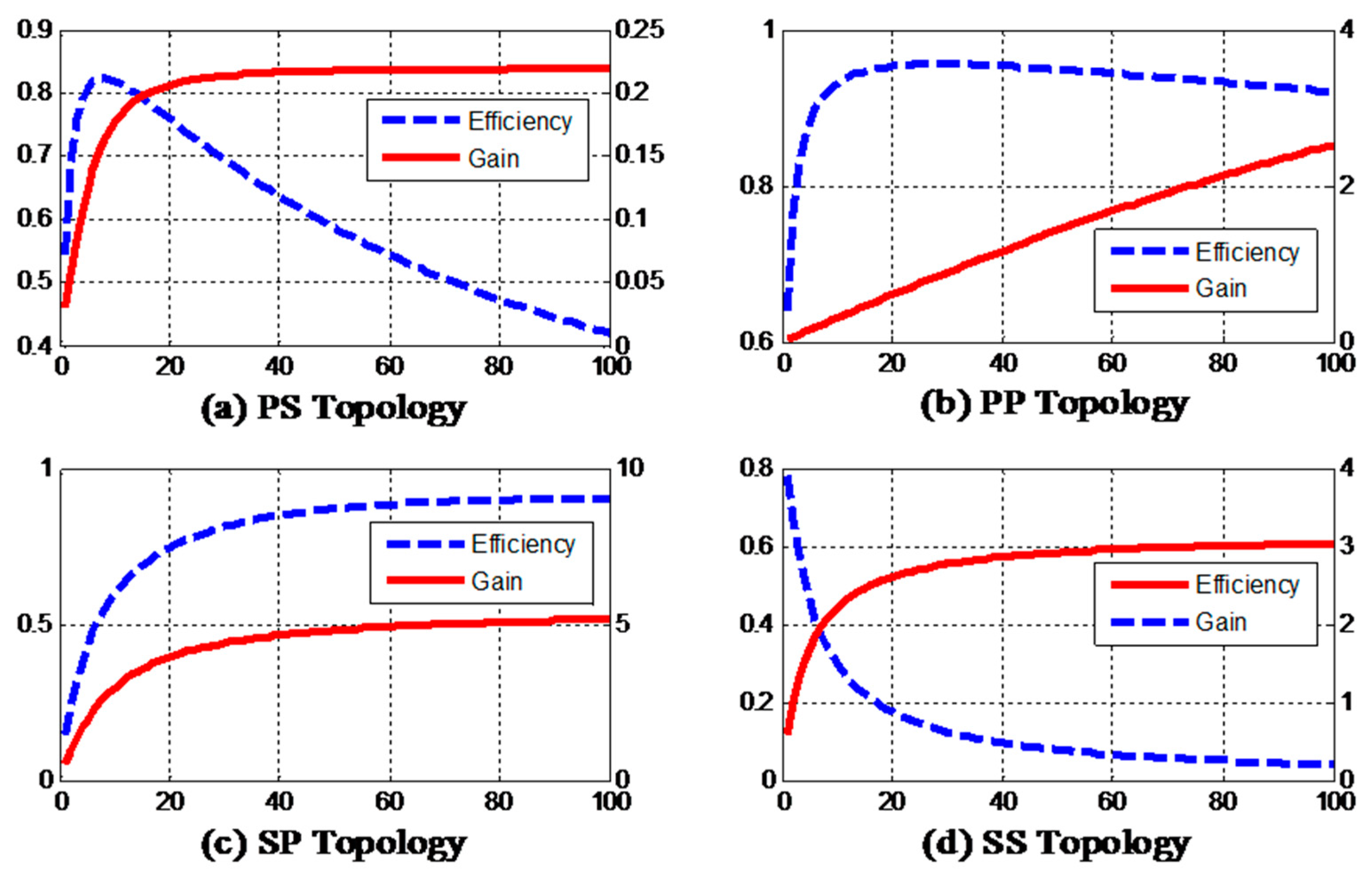
In order to compare this topology performance with traditional WPT system, this chapter presents the voltage gain of four resonant networks (PP, PS, SP and SS) with the same resonant parameters. The voltage gain and efficiency of four compensation circuits are compared against load variation range from 0 to 100 Ω in Figure 7.
In Figure 7, for secondary series topology including PS and SS, this kind of topology cannot achieve high voltage gain due to its voltage source characteristic, and its efficiency is relatively low on the light load condition. Secondary parallel topology can achieve relatively high voltage gain (maximum gain equals 5.1) due to its current source characteristic, but voltage gain varies greatly with load variation. For heavy load conditions, its voltage gain is low.
Compared with the four basic compensation circuits, the proposed push–pull circuit can operate at an adjustable gain versus load R with high efficiency from the analyses A and B.
5. Experimental Verification
For the sake of verifying the performance of the proposed topology, a prototype system is built up. The system has been constructed according to the parameters provided in Table 1 and the device photo is shown in Figure 8.
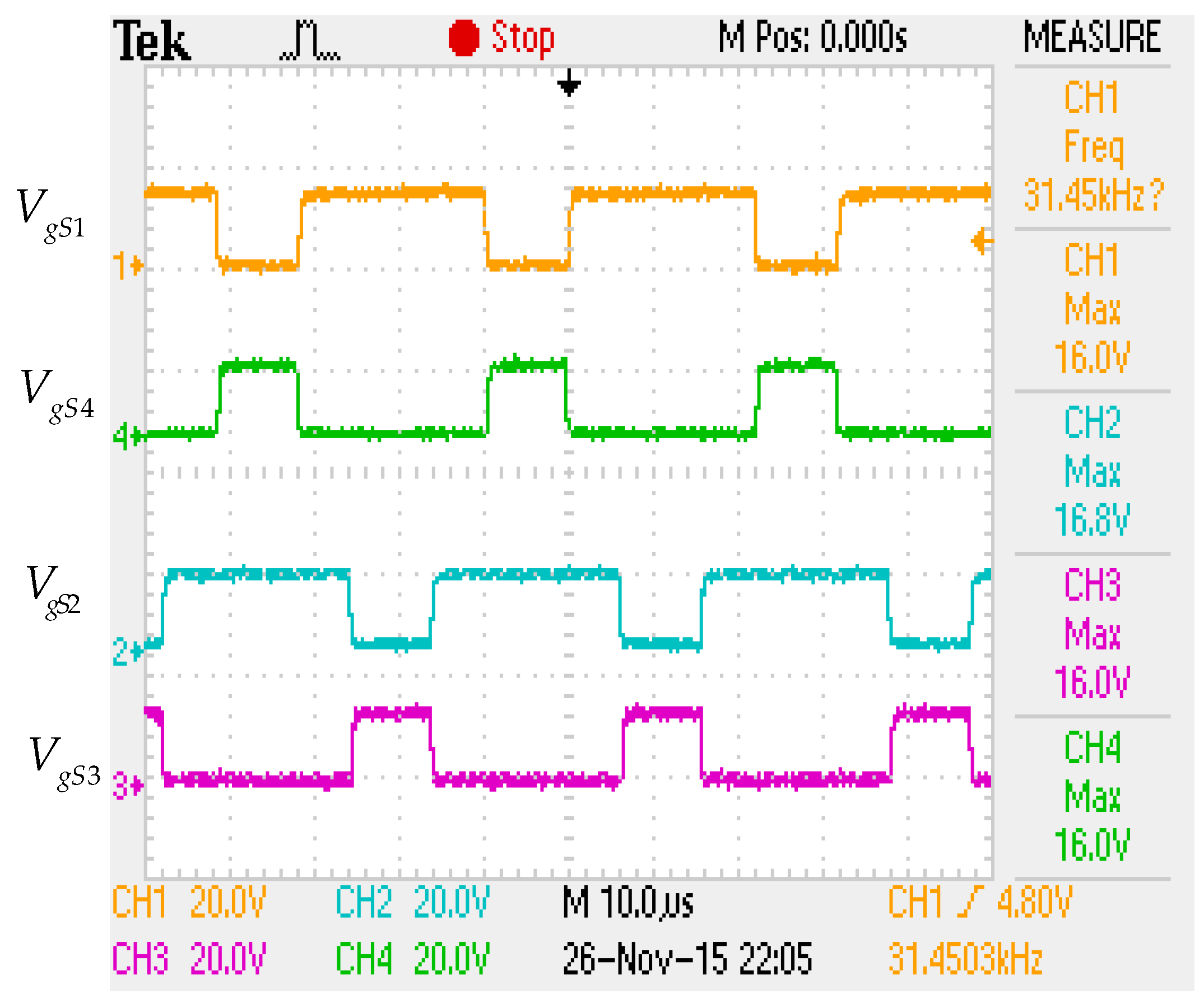
Figure 9 shows the waveforms of the push–pull switches gate-driving signals and anti-series switching gate-driving signals. The resonant voltage VCP and resonant current ILP are shown in Figure 10 and the resonant voltage and current waveforms are sinusoidal waves, which indicate that the system can work under the state of resonance.
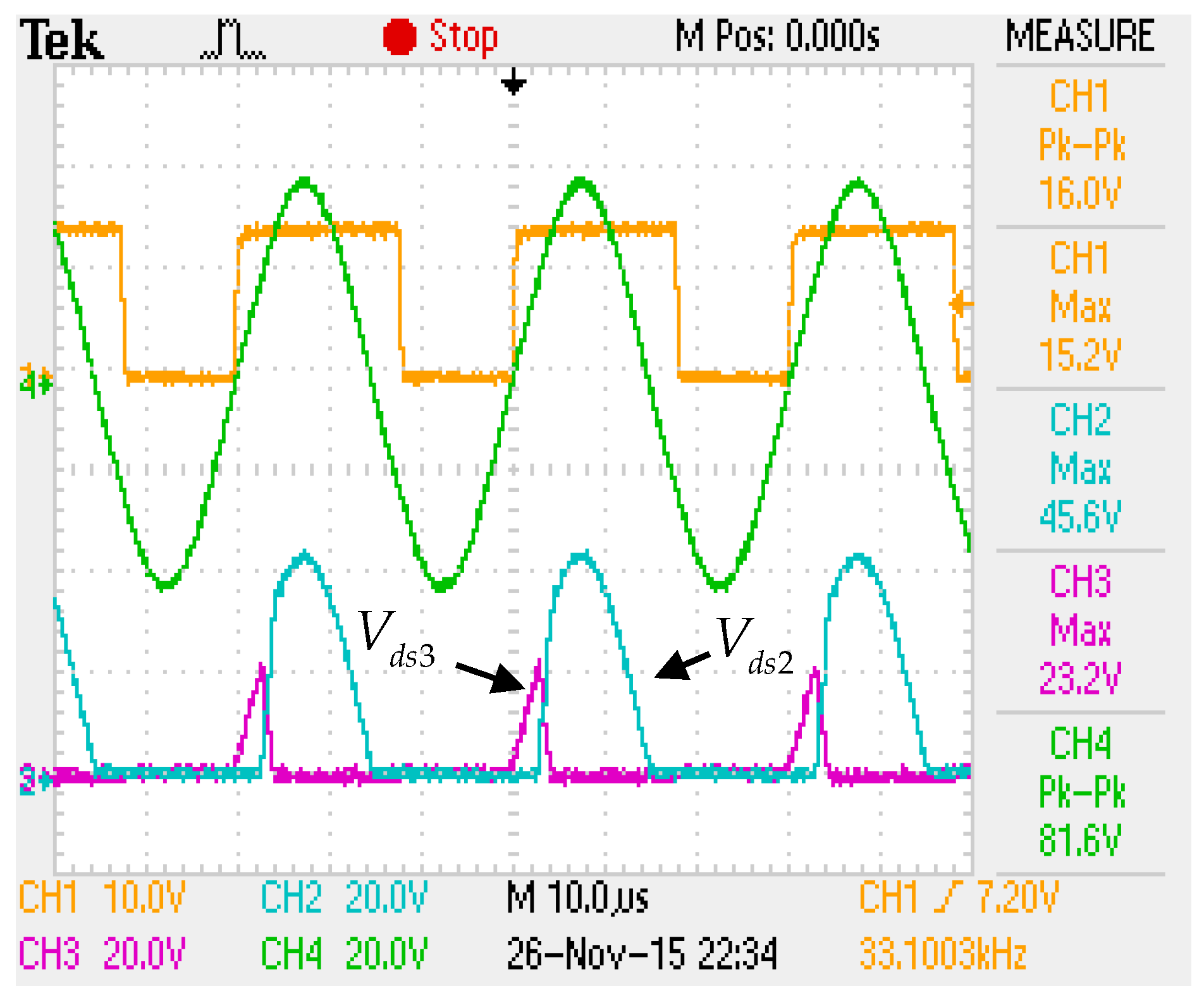
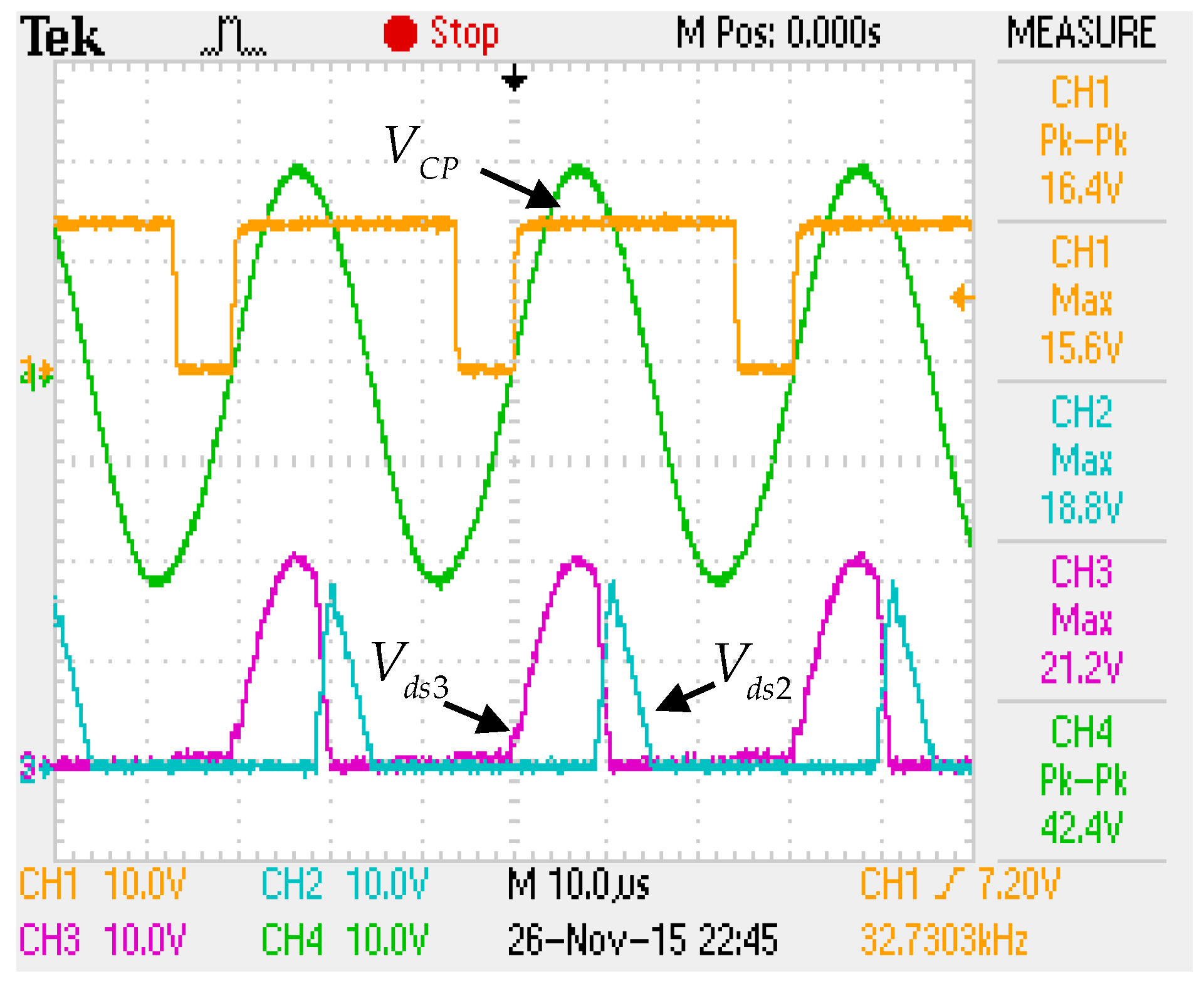
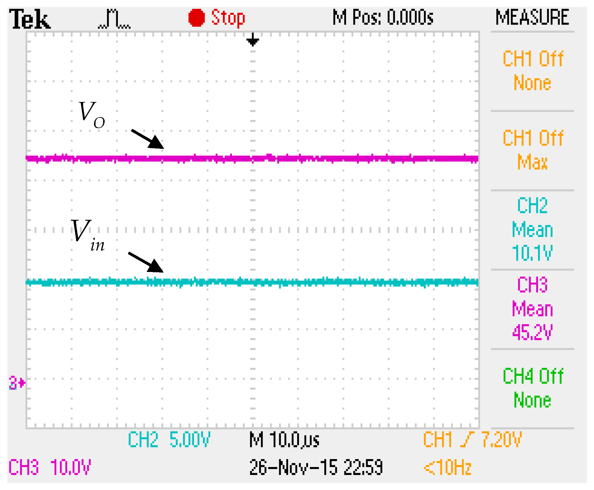
Figure 11 shows the waveforms of VdS2, VdS3 and VCP from top to bottom. It can be seen that the synthesized waves of VdS2 and VdS3 are exactly half of the resonant wave VCP on the condition of D = 0.6. The same result can be detected that the synthesized waves of VdS1 and VdS4 are exactly half of the resonant wave VCP. When the duty cycle becomes D = 0.8, the waveforms of VdS2, VdS3 and VCP are shown in Figure 12 and VdS2 and VdS3 are changing when the duty cycle D is changing. Figure 13 shows that VO is controlled at 43 V for the condition of R = 50 Ω and D = 0.8, which achieves a gain of 4.3 times compared with the input voltage Uin = 10 V. It verifies that the system can realize a higher gain by regulating the duty cycle D.
Table 2 presents the experimental data of the proposed topology. The controlled gain range is from 1.6 to 7.3. With higher gain, the system can get higher output power. Furthermore, system efficiency can remain above 80%. Figure 14 shows that the experimental results of voltage gain match with the theoretical results well, except that there is little difference at the maximum gain point. It is because power losses at the primary side will increase at the top gain point.
6. Discussion
In order to present a close loop control of the voltage gain, a Proportion Integration Differentiation (PID) control is applied to regulate the duty cycle D of the switches. The close loop control structure can be shown in Figure 15.
The information of output voltage VO is measured and sent back to the primary side by an Radio Frequency (RF)-link. Furthermore, a PID controller is utilized to control the duty cycle of S3 and S4, according to the difference between VO and Vref.
A load switching test was carried out to evaluate the controller’s performance. In this test, load condition is set to switching between 10 Ω and 30 Ω. The DC input voltage is set at 5 V. The output reference voltage is set at 20 V. The experimental result can be shown in Figure 16.
As can be seen in Figure 16, there are two load switching events in the control process: one is from 20 Ω to 10 Ω (first switching) and the other is from 10 Ω to 20 Ω (second switching). In the control process, the output voltage is kept stable except for some switching disturbance. The experimental results verify the close loop control performance of the PID controller.
7. Conclusions
In order to achieve controllable high voltage gain output, this paper proposed a novel current-fed push–pull topology for the WPT system. This method utilizes a bi-directional switch that is added to isolate the inverter with resonant network and guide the power flow into the resonant tank. On the basis, an energy storage and injection switching mode is proposed to enhance voltage gain. A switching duty cycle is also proposed to implement gain control. This method can greatly improve the voltage gain in the WPT system and maintain a high system efficiency at the same time. This is important for low DC voltage input application including PV power supply and USB charger.
Acknowledgments
This research works is support by the National Natural Science Foundation of China (51377187, 51377183) and the Chongqing International Science and Technology Cooperation Base Project (CSTC2015GJHZ40001).
Author Contributions
The main idea of this paper is proposed by Qichang Duan and Yanling Li. Yanling Li wrote this paper. Xin Dai gave experiment design. Tao Zou performed verification experiments.
Conflicts of Interest
The authors declare no conflict of interest.
References
- Geng, Y.; Yang, Z.; Lin, F.; Hu, S. A High Efficiency Charging Strategy for a Supercapacitor Using a Wireless Power Transfer System Based on Inductor/Capacitor/Capacitor (LCC) Compensation Topology. Energies 2017, 10, 135. [Google Scholar] [CrossRef]
- Jinwook, K.; Hyeon-Chang, S.; Do-Hyeon, K. Optimal Design of a Wireless Power Transfer System with Multiple Self-Resonators for an LED TV. IEEE Trans. Consum. Electron. 2012, 58, 775–780. [Google Scholar]
- RamRakhyani, A.K.; Lazzi, G. On the Design of Efficient Multi-Coil Telemetry System for Biomedical Implants. IEEE Trans. Biomed. Circuits Syst. 2013, 7, 11–23. [Google Scholar] [CrossRef] [PubMed]
- Dai, X.; Sun, Y. An Accurate Frequency Tracking Method Based on Short Current Detection for Inductive Power Transfer System. IEEE Trans. Ind. Electron. 2014, 61, 776–783. [Google Scholar] [CrossRef]
- Zou, Y.; Dai, X.; Li, W.; Sun, Y. Robust Design Optimization for Inductive Power Transfer Systems from Topology Collection Based on an Evolutionary Multi-Objective Algorithm. IET Power Electron. 2015, 8, 1767–1776. [Google Scholar] [CrossRef]
- Ho, Y.L.; Budgett, D.M.; Hu, A.P. Minimizing Power Loss in Air-Cored Coils for TET Heart Pump Systems. IEEE J. Emerg. Sel. Top. Circuits Syst. 2011, 1, 412–419. [Google Scholar]
- Kuo, N.C.; Zhao, B.; Niknejad, A.M. Bifurcation Analysis in Weakly-Coupled Inductive Power Transfer Systems. IEEE Trans. Circuits Syst. I Regul. Pap. 2016, 63, 727–738. [Google Scholar] [CrossRef]
- Hu, A.P.; You, Y.W.; Chen, F.B. Wireless Power Supply for ICP Devices with Hybrid Supercapacitor and Battery Storage. IEEE J. Emerg. Sel. Top. Power Electron. 2016, 4, 273–279. [Google Scholar] [CrossRef]
- Jittakort, J.; Yachiangkam, S.; Sangswang, A. A Variable-frequency Asymmetrical Voltage-Cancellation Control of Series Resonant Inverters in Domestic Induction Cooking. In Proceedings of the 2011 IEEE 8th International Conference on Power Electronics and ECCE Asia (ICPE 2011-ECCE Asia), Jeju, Korea, 30 May–3 June 2011; pp. 2320–2327. [Google Scholar]
- Kim, N.Y.; Kim, K.Y.; Choi, J. Adaptive Frequency with Power-Level Tracking System for Efficient Magnetic Resonance Wireless Power Transfer. Electron. Lett. 2012, 48, 452–454. [Google Scholar] [CrossRef]
- Huanmin, W.; Hui, Z.; Yanting, L. Analysis on Wireless Charging Circuit Characteristic Under The Hybrid Compensation Topology. In Proceedings of the 2016 IEEE 8th International Power Electronics and Motion Control Conference (IPEMC 2016-ECCE Asia), Hefei, China, 22–26 May 2016; pp. 2450–2454. [Google Scholar]
- Dai, X.; Zou, Y.; Sun, Y. Uncertainty Modeling and Robust Control for LCL Resonant Inductive Power Transfer System. J. Power Electron. 2013, 13, 814–828. [Google Scholar] [CrossRef]
- Neath, M.J.; Swain, A.; Madawala, U. An Optimal PID Controller for a Bidirectional Inductive Power Transfer System Using Multi-objective Genetic Algorithm. IEEE Trans. Power Electron. 2013, 29, 1523–1531. [Google Scholar] [CrossRef]
- Gao, Y.; Farley, K.B.; Tse, Z.T. A uniform voltage gain control for alignment robustness in wireless EV charging. Energies 2015, 8, 8355–8370. [Google Scholar] [CrossRef]
- Abdolkhani, A.; Hu, A.P. A Novel Detached Magnetic Coupling Structure for Contactless Power Transfer. In Proceedings of the 37th Annual Conference of IEEE Industrial Electronics (IECON 2011), Melbourne, Australia, 7–10 November 2011; pp. 1103–1108. [Google Scholar]
- Hou, J.; Chen, Q.; Yan, K.; Ren, X.; Wong, S.C.; Tse, C.K. Analysis and Control of S/Sp Compensation Contactless Resonant Converter with Constant Voltage Gain. In Proceedings of the 2013 IEEE Energy Conversion Congress and Exposition (ECCE), Denver, CO, USA, 15–19 September 2013; pp. 2552–2558. [Google Scholar]
Figure 1.
High controllable voltage gain push–pull topology.

Figure 2.
Operation principle of the push–pull topology.

Figure 3.
Operating modes of the proposed circuit in one cycle. (a) Mode I; (b) Mode II; (c) Mode III; and (d) Mode IV.
Figure 3.
Operating modes of the proposed circuit in one cycle. (a) Mode I; (b) Mode II; (c) Mode III; and (d) Mode IV.

Figure 4.
Equivalent circuit of the push–pull circuit.

Figure 5.
Influence of load R: (a) Output gain with various load R; (b) System efficiency with load R.
Figure 5.
Influence of load R: (a) Output gain with various load R; (b) System efficiency with load R.

Figure 6.
Influence of coupling coefficient: (a) Output gain; (b) System efficiency.

Figure 7.
Gain and efficiency of four basic compensation circuits.

Figure 8.
Experimental system photo.

Figure 9.
Gate-driving signals’ waveforms.

Figure 10.
Resonant voltage and resonant current waveforms.

Figure 11.
Waveforms of VdS2, VdS3 and VCp at D = 0.6.

Figure 12.
Waveforms of VdS2, VdS3 and VCp at D = 0.8.

Figure 13.
Waveforms of input voltage and output voltage.

Figure 14.
Comparison of the system gain curve.

Figure 15.
Close loop control.

Figure 16.
Experimental results of close loop control.


Table 1.
System parameters.
| Parameters | Values |
|---|---|
| Resonant frequency f (KHz) | 31.45 |
| Primary resonant inductor LP () | 30.38 |
| Primary inductor resistance RP () | 0.025 |
| Primary capacitor CP () | 0.66 |
| Secondary resonant inductor LS () | 36.82 |
| Secondary inductor resistance RS () | 0.029 |
| Secondary resonant capacitor CS () | 0.57 |
| Coupling coefficient k | 0.157 |
| System load R () | 50 |
Table 2.
Experiment Results.
| Input Voltage/Current (V/A) | Duty Cycle of S1 (D) | Output Voltage (V) | Output Power (W) | Gain | Efficiency |
|---|---|---|---|---|---|
| 10/0.61 | 0.5 | 16.2 | 5.4 | 1.6 | 88% |
| 10/1.09 | 0.6 | 21.7 | 9.5 | 2.17 | 87.4% |
| 10/1.96 | 0.7 | 28.9 | 16.9 | 2.89 | 86% |
| 10/2.80 | 0.75 | 34.5 | 23.8 | 3.45 | 85% |
| 10/4.7 | 0.8 | 43.1 | 39.5 | 4.31 | 84.1% |
| 10/8.08 | 0.85 | 53.8 | 67.5 | 5.38 | 83.6% |
| 10/15.2 | 0.9 | 72.3 | 123 | 7.3 | 80.9% |
© 2017 by the authors. Licensee MDPI, Basel, Switzerland. This article is an open access article distributed under the terms and conditions of the Creative Commons Attribution (CC BY) license (http://creativecommons.org/licenses/by/4.0/).
Share and Cite
MDPI and ACS Style
Duan, Q.; Li, Y.; Dai, X.; Zou, T. A Novel High Controllable Voltage Gain Push-Pull Topology for Wireless Power Transfer System. Energies 2017, 10, 474. https://doi.org/10.3390/en10040474
AMA Style
Duan Q, Li Y, Dai X, Zou T. A Novel High Controllable Voltage Gain Push-Pull Topology for Wireless Power Transfer System. Energies. 2017; 10(4):474. https://doi.org/10.3390/en10040474
Chicago/Turabian StyleDuan, Qichang, Yanling Li, Xin Dai, and Tao Zou. 2017. "A Novel High Controllable Voltage Gain Push-Pull Topology for Wireless Power Transfer System" Energies 10, no. 4: 474. https://doi.org/10.3390/en10040474
Note that from the first issue of 2016, this journal uses article numbers instead of page numbers. See further details here.