
Double-Carrier Phase-Disposition Pulse Width Modulation Method for Modular Multilevel Converters


1
College of Electrical and Information Engineering, Hunan University, Changsha 410082, China
2
School of Information Science and Engineering, Central South University, Changsha 410083, China
3
Department of Energy Technology, Aalborg University, Aalborg East DK-9220, Denmark
*
Author to whom correspondence should be addressed.
Energies 2017, 10(4), 581; https://doi.org/10.3390/en10040581
Submission received: 12 February 2017
/
Revised: 10 April 2017
/
Accepted: 20 April 2017
/
Published: 23 April 2017
(This article belongs to the Special Issue Distribution Power Systems and Power Quality)
Abstract
:Modular multilevel converters (MMCs) have become one of the most attractive topologies for high-voltage and high-power applications. A double-carrier phase disposition pulse width modulation (DCPDPWM) method for MMCs is proposed in this paper. Only double triangular carriers with displacement angle are needed for DCPDPWM, one carrier for the upper arm and the other for the lower arm. Then, the theoretical analysis of DCPDPWM for MMCs is presented by using a double Fourier integral analysis method, and the Fourier series expression of phase voltage, line-to-line voltage and circulating current are deduced. Moreover, the impact of carrier displacement angle between the upper and lower arm on harmonic characteristics is revealed, and further the optimum displacement angles are specified for the circulating current harmonics cancellation scheme and output voltage harmonics minimization scheme. Finally, the proposed method and theoretical analysis are verified by simulation and experimental results.
1. Introduction
Nowadays, modular multilevel converters (MMCs) have become one of the most attractive multilevel converter topologies available for high-voltage and high-power applications such as voltage-sourced converter high-voltage direct current (VSC-HVDC) transmission [1,2,3,4,5,6], static synchronous compensators (STATCOMs) [7], unified power flow controllers (UPFCs) [8], active power filters (APFs) [9], medium voltage motor drives [10], integration of renewable energy sources into the electrical grid [11,12,13] and battery energy storage systems [14,15]. Compared to other multilevel converter topologies, the salient features of MMC include: high degree of modularity, high efficiency, superior harmonic performance, high reliability and absence of dc-link capacitors [5].
Many academic papers have focused on modeling [16,17,18,19], control [20,21,22,23,24], and modulation techniques [25,26,27,28,29,30,31,32,33,34,35,36,37,38,39,40,41] for MMCs. The multilevel converter pulse width modulation technique is one of the key technologies for MMCs as it affects the harmonic characteristics, voltage balancing and system efficiency. Various pulse width modulation techniques have been applied for MMCs, and each technique has advantages and drawbacks [25,26]. The selective harmonic elimination-pulse width modulation (SHE-PWM) method can provide good harmonic features with low switching frequency of sub-modules (SMs). However, the calculation of angles increases significantly as the number of output voltage levels increases [27,28,29]. The space vector modulation (SVM) method can provide more flexibility to optimize switching waveforms. However, when the number of voltage levels increases, the complexity of the algorithm for SVM grows exponentially [4]. In [30], a simplified SVM scheme was proposed for MMCs, which reduces the computation demands and can be used for any level MMC. The main advantage of the nearest level modulation (NLM) method is its simple implementation. However, the NLM method generates poor quality waveforms with small numbers of SMs [31,32]. The application scope of NLM is extended by introducing one SM operating in the PWM mode [33,34]. The phase-shifted carrier pulse-width modulation (PSCPWM) method achieves even power distribution among the SMs [35,36]. However, dedicated capacitor voltage balancing controllers for each SM are mandatory, which reduces the harmonic performance of the output voltage. Compared with PSCPWM, the phase-disposition pulse width modulation (PDPWM) method has superior harmonic characteristics by placing significant harmonic energy into the first carrier component in the phase voltage and relying upon the elimination of this component when the line-to-line voltages are created [25]. The main drawback of the PDPWM is the uneven loss distribution among the SMs, which can be solved by the voltage balancing method based on sorting [37,38,39,40]. In [41], an improved PDPWM method using a single carrier was proposed for MMCs, which reduces the control hardware requirement. However, the upper arm and lower arm use the same carrier, and the impact of the carrier displacement angle between the upper arm carrier and the lower arm carrier on the harmonic characteristics has not been considered. The circulating current and output voltage for MMCs are determined by the interactions between the upper arm voltage and the lower arm voltage [42]. Therefore, the carrier for the lower arm and the carrier for the upper arm need to be analyzed separately with an interleaved displacement angle. The displacement angle will influence the high-frequency interactions between the upper arm and lower arm, and further affect the harmonic characteristics of MMCs [43].
A double-carrier phase-disposition pulse width modulation (DCPDPWM) method for MMC is proposed in this paper. Only double triangular carriers with displacement angle are needed for DCPDPWM, one carrier for the upper arm and the other for the lower arm. The theoretical analysis of DCPDPWM for MMC is presented based on double Fourier integral analysis method, and the Fourier series expression of phase voltage, line-to-line voltage and circulating current are deduced. Moreover, the impact of carrier displacement angle between the upper and lower arms on harmonic characteristics is revealed, and the optimum displacement angles are specified for the circulating current harmonics cancellation scheme and output voltage harmonics minimization scheme.
The paper is organized as follows: Section 2 introduces the topology and mathematical model of MMC. Section 3 proposes the DCPDPWM method for MMC. Section 4 presents the theoretical analysis of DCPDPWM for MMC by using double Fourier integral analysis method, and the optimum displacement angles are specified for the circulating current harmonics cancellation scheme and output voltage harmonics minimization scheme. Section 5 and Section 6 show the simulation and experimental results, respectively. The conclusions are summarized in Section 7.
2. Topology and Mathematical Model of MMC
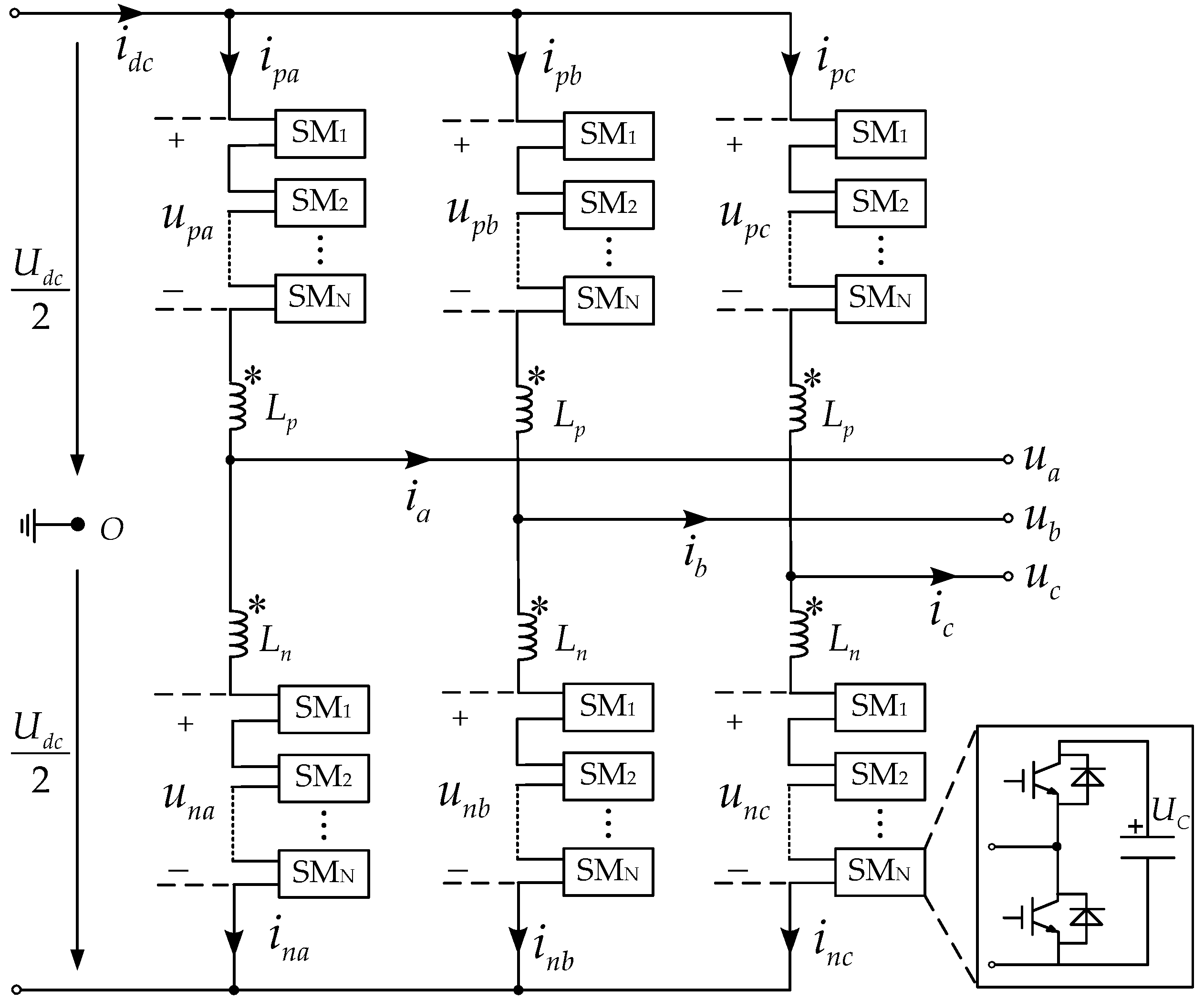
The schematic diagram of a three phase MMC is shown in Figure 1. The MMC comprises upper and lower arms per phase-leg. Each arm consists of N series-connected, nominally identical SMs and a series buffer inductor. The buffer inductors for the upper and lower arms can be chosen as coupled or separate ones. The coupled inductor is adopted in this paper as it has lighter weight and smaller size than two separate inductors [34,35]. The power loss of SMs and the resistances of the inductors are ignored. Based on Kirchhoff’s voltage law, the following equations can be obtained:
where Udc is the dc-link voltage. uj denotes the output voltage phase-j (j = a, b, c). upj and unj are the output voltage of the upper and the lower arms, respectively. ipj and inj refer to the current of the upper arm and the lower arm, respectively. Lp and Ln are the self-inductances of the coupling inductance for the upper and lower arms, respectively. Mu is the mutual inductance, assuming the two inductors are closely coupled and the leakage inductance can be ignored (i.e., Lp = Ln = Mu = L).
According to Kirchhoff’s current law, the upper and lower arm current of phase-j can be expressed as:
where ij and icj are the output current and circulating current of phase-j, respectively.
Combining (1)–(4), the output voltage and circulating current of phase-j can be derived as:
Combining (1), (2) with (6), the following equation can be obtained as:
According to (7), the circulating current of phase-j can be calculated as:
where Icj is the dc component of circulation current icj.
3. Implementation of Double-Carrier Phase Disposition Pulse Width Modulation for MMCs
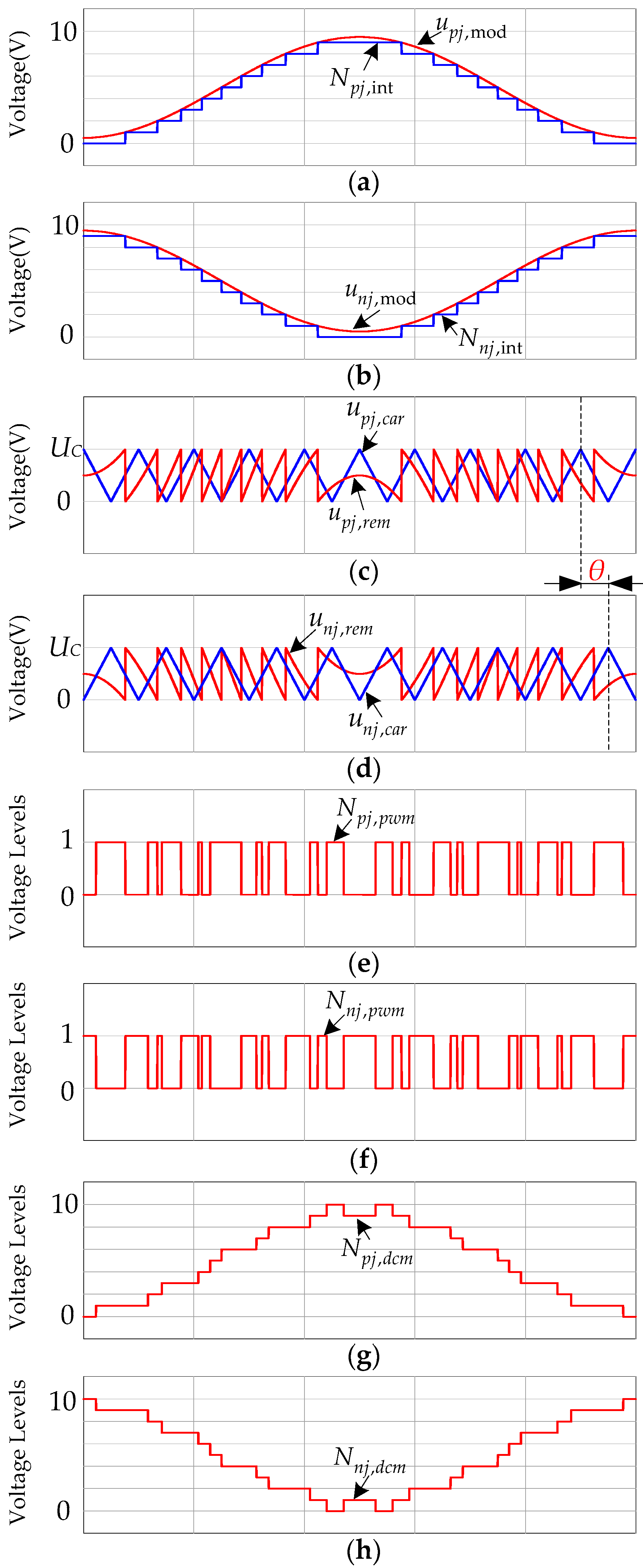
The principle of DCPDPWM for MMCs is shown in Figure 2, where N is the number of SMs for each arm (e.g., N = 10). Only two carriers with displacement angle are needed for DCPDPWM, one carrier for the upper arm and the other for lower arm. Where θ is defined as the displacement angle between the upper arm carrier and lower arm carrier, and the range of θ can be obtained as [0, 2π). Note that the displacement angle θ between upper arm carrier and lower arm carrier has a significant impact on the harmonic characteristics of MMC, which will be analyzed in Section 4.
The reference voltages of the upper and lower arm for phase-j can be expressed as:
where M (0 < M ≤ 1) denotes the modulation index. ωo is the angular frequency of output voltage. is the phase angle of phase-j ( = 0, = –2π/3, = 2π/3).
The modulation signals of the upper and lower arms for phase-j can be obtained as:
where UC is the capacitor rated voltage of SMs. Given that UC = Udc/N. The range of modulation signals are [−N/2, N/2].
As shown in Figure 2a,b, the integer portion of upper arm and low arm modulation signals can be calculated as:
In which the function floor(x) obtains the largest integer that is less than or equal to x. Npj,int, Nnj,int are the integer portion of modulation signals, respectively.
As shown in Figure 2c,d, the remainder of reference voltage for upper and lower arms can be derived as:
where upj,rem and unj,rem are the remainder of reference voltage for upper arm and lower arm, respectively.
The expressions of upper and the lower arms carriers can be obtained as:
where upj,car and unj,car are the carriers of upper and lower arms, respectively. k is the number of carrier period (k ∈ [0, 1, ..., n]). ωc is the angular frequency of triangular carrier.
As shown in Figure 2e,f, the PWM signals of upper and lower arms can be obtained by comparing the remainders with the carriers of upper and lower arms, respectively. The PWM signals of upper and lower arms can be calculated as:
As shown in Figure 2g,h, the number of on-state SMs for each arm can be obtained by adding the integer portion and corresponding PWM portion. The number of on-state SMs for upper and lower arms can be obtained as:
where Npj,dcm, Nnj,dcm are the number of on-state SMs for upper and lower arms, respectively.
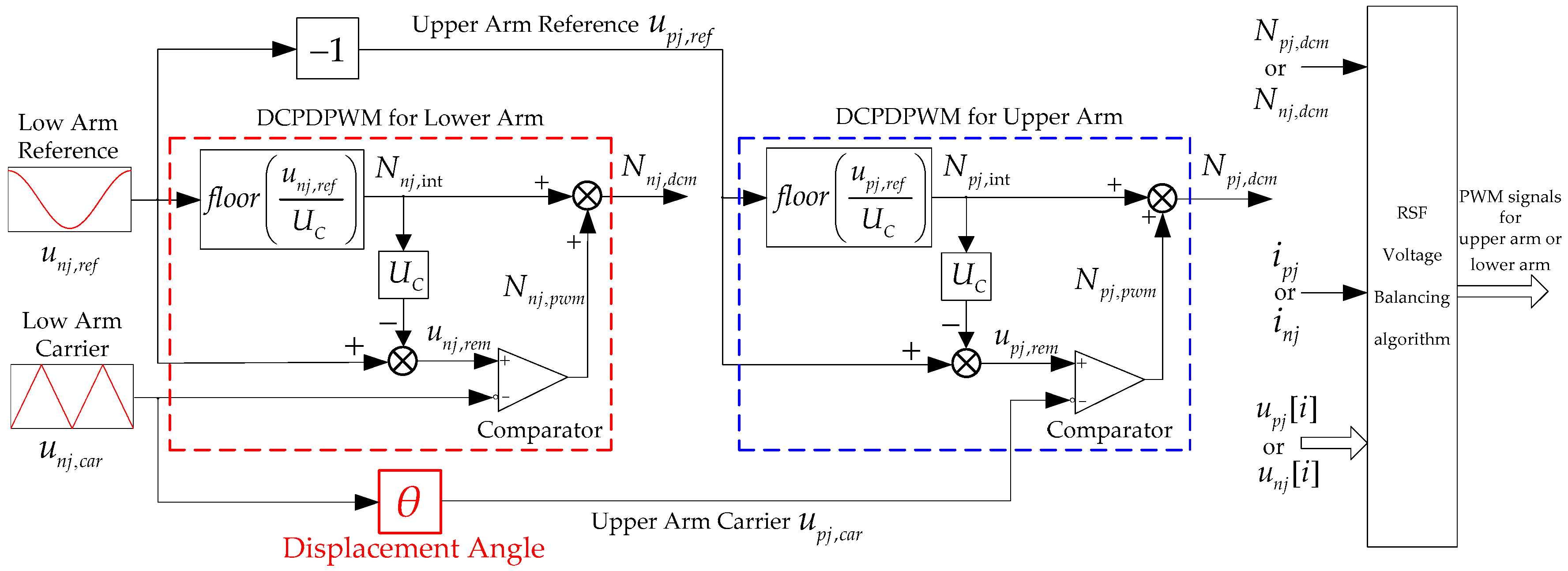
The block diagram of double-carrier phase-disposition pulse width modulation with a capacitor voltage balancing algorithm is shown in Figure 3. Firstly, the number of on-state SMs for each arm is obtained through the DCPDPWM. Then, the selection of the SMs is performed based on the reducing switching frequency (RSF) voltage balancing algorithm [44], which can achieve capacitor voltage balancing of SMs and reduce the average device switching frequency. upj[i] (i = 1, 2, …, N) and unj[i] are the capacitor voltages of SMs for the upper and lower arms, respectively.
As the circulating current control can influence several performance features of MMCs such as suppressing the low frequency circulating current, increasing the switching frequency, reducing the capacitor voltage ripple and so on, for simplicity, it is assumed that the circulating current control method is not applied in the block diagram as shown in Figure 3. Note that this assumption is reasonable as the circulating currents flowing through the three phase legs of the MMC caused by the voltage differences among the dc-link voltage and three phase legs, which will not affect the output voltages and currents [5,22]. Moreover, this paper mainly focuses on the high frequency (switching frequency) circulating current caused by DCPDPWM method for MMCs, whereas the circulating current control method focuses on low frequency circulating currents (mainly second-order harmonic currents), which can be suppressed by adding a circulating current control method [36,43]. Thus the circulating current control method affects significantly the low frequency harmonic circulating current and has a relatively small influence on switching frequency circulating current. The switching frequency harmonics caused by circulating current control method can be suppressed by selecting the arm inductance properly [24].
4. Theoretical Analysis of DCPDPWM Method for MMCs
The double Fourier integral analysis method is the most well-known analytical method for determining the harmonic components of a PWM method [45]. In this section, the theoretical analysis of DCPDPWM for MMCs is presented using the double Fourier integral analysis method. The Fourier series expression of phase voltage, line-to-line voltage and circulating current are deduced. Moreover, the influence of carrier displacement angle between upper and lower arms on the harmonic characteristics is revealed, and the optimum displacement angles are specified for the circulating current harmonics cancellation scheme and output voltage harmonics minimization scheme.
4.1. Influence of the Carrier Displacement Angle on Harmonic Characteristic of Output Voltage and Circulating Current for MMC
Note that the following harmonics analysis focuses on the switching harmonics produced by DCPDPWM, while the low-frequency harmonics (e.g., second-order harmonic for circulating current) caused by the energy oscillation between the upper arm and lower arm are not included.
Assuming N is even, and the range of modulation index M can be obtained as [0, 1]. For simplicity, it is assumed that the capacitance of each submodule is large enough and all the capacitor voltages of SMs are naturally balanced (i.e., UC = Udc/N), so that the capacitor voltage ripple can be ignored. Note that this assumption is reasonable as the capacitor voltage ripple is generally a relatively small portion comparing with the reference voltages of upper and lower arms [36,43].
The analytical technique for determining the spectral components of multilevel PWM method proposed in [46,47] is applied for DCPDPWM. The phase voltage can be derived as follows (see Appendix A):
where m denotes the carrier index variable and n refers to the baseband index variable.
The line-to-line voltage can be calculated as:
Substituting (23) and (24) into (7), the circulating current can be obtained as:
The magnitudes of carrier harmonic components and associated sideband harmonic components for the phase voltage, line-to-line voltage, circulating current can be expressed as follows:
where:
where Uj,m,n, Ull,m,n and Icj,m,n are the magnitudes of carrier harmonic components and associated sideband harmonic components for the phase voltage, line-to-line voltage and circulating current, respectively. ωj, ωll, and ωcj are the angular frequency of phase voltage, line-to-line voltage and circulating current, respectively.
As shown in Equations (23)–(30), the phase voltage consists of a fundamental component, odd carrier harmonic components, even sideband harmonic components of odd carrier groups, and odd sideband harmonic components of even carrier groups. The carrier harmonic components and triple sideband harmonic components are cancelled in the line-to-line voltage. The circulating current consists of dc component, odd carrier harmonic components, even sideband harmonic components of odd carrier groups, and odd sideband harmonic components of even carrier groups.
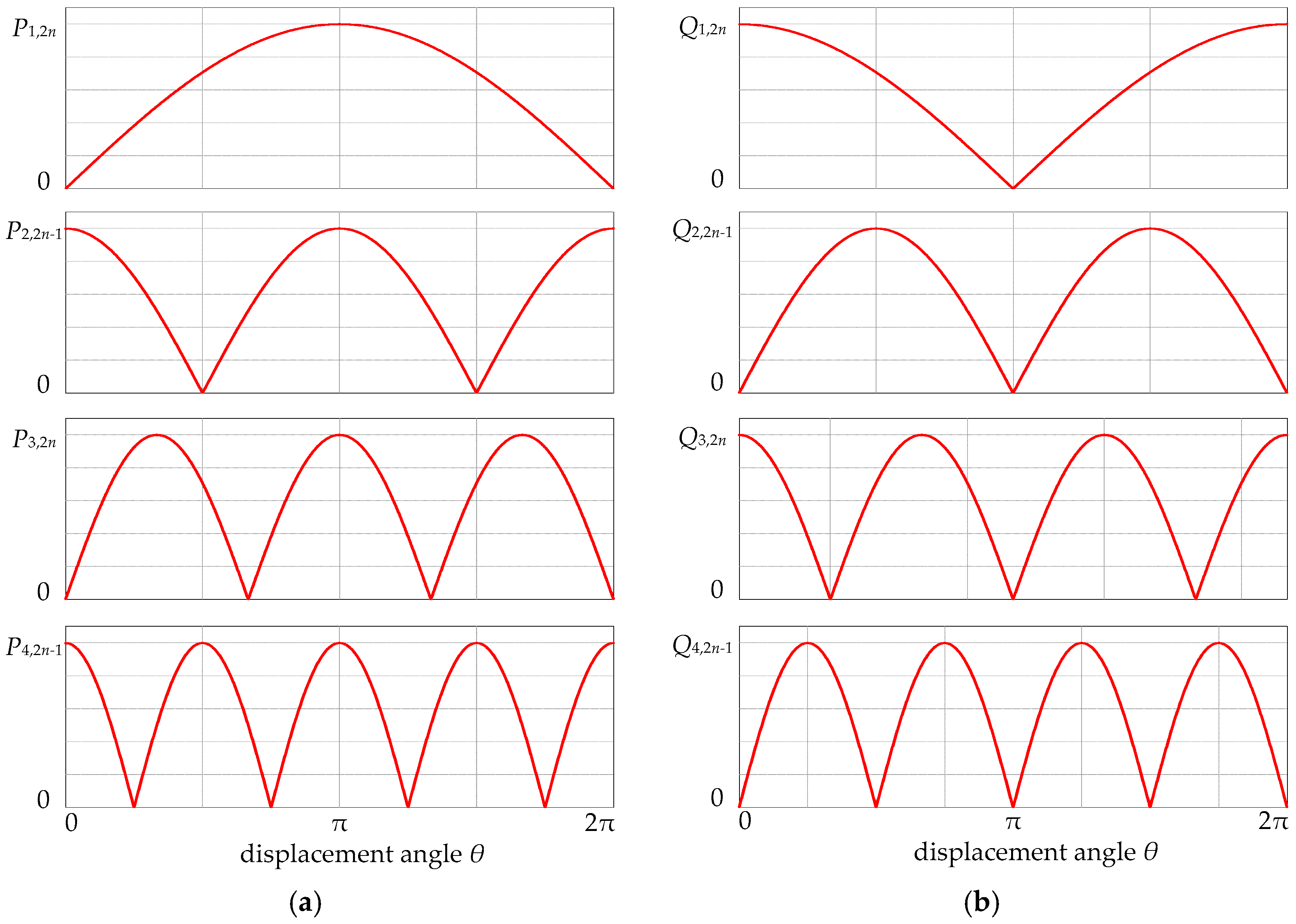
It can be seen that the magnitudes of carrier harmonic components and associated sideband harmonic components for the phase voltage, line-to-line voltage and the circulating current are the function of displacement angle θ, respectively. Figure 4 shows the magnitudes of the harmonic components for the phase voltage and circulating current with different displacement angles. Only the first four harmonic groups (m ≤ 4) are studied here due to the limitations of the paper. Where P1,2n, P2,2n-1, P3,2n, P4,2n-1 and Q1,2n, Q2,2n-1, Q3,2n, Q4,2n-1 are the maximums of the first four harmonic groups for phase voltage and circulating current, respectively.
It is found that the changing tendency of the magnitudes for harmonic components in the phase voltage and circulating current are opposite. When the magnitudes of harmonic components for phase voltage and line-to-line voltage are at their minima, the magnitudes of the harmonic components for the circulating current are maximum, and vice versa. Therefore, the displacement angle θ should be specified according to the specific industry application. When the number of SMs for each arm is large, such as in HVDC applications, superior harmonics characteristics of the output voltage can be achieved, so reducing the harmonics of the circulating current is the main problem. On the other hand, when the number of SMs for each arm is small, such as in STATCOM and motor drive applications, reducing the harmonics of the output voltage is preferred.
4.2. Circulating Current Harmonics Cancellation Scheme for DCPDPWM Method
When displacement angle θ = π, the circulating current harmonics cancellation scheme for DCPDPWM can be obtained. According to (23), the phase output voltage can be obtained as:
According to (24), the line-to-line voltage can be expressed as:
According to (25), the circulating current can be derived as:
It can be seen that the magnitudes of the carrier harmonic components and associated sideband harmonic components for the circulating current are zero, which means that the carrier harmonic components and associated sideband harmonic components of the circulating current caused by DCPDPWM are completely cancelled out, leaving only the dc component. Therefore, the power loss and arm current stress are decreased. However, the magnitudes of the carrier harmonic components and sideband harmonic components for the phase voltage are at their maxima. The equivalent switching frequency (frequency of the lowest harmonic group) is fdcm, where fdcm denotes the carrier frequency of DCPDPWM.
4.3. Output Voltage Harmonics Minimization Scheme for the DCPDPWM Method
When carrier displacement angle θ = 0, the output voltage harmonics minimization scheme for DCPDPWM can be obtained. According to (23), the phase output voltage can be derived as:
According to (24), the line-to-line output voltage can be obtained as:
According to (25), the circulating current can be derived as:
It can be seen that the odd carrier harmonic components and the even sideband harmonic components of odd carrier groups for phase voltage are completely cancelled, leaving only the odd sideband harmonic components of even carrier groups. The equivalent switching frequency of phase voltage increases to 2 × fdcm, which means that the better harmonic characteristics can be achieved for phase voltage and current. However, the magnitudes of odd carrier harmonic components and even sideband harmonic components of odd carrier groups for circulating current are maximized, which increases the current stress upon the power semiconductor devices and decreases the MMC efficiency.
When the carrier displacement angle θ = 0, the carrier for the upper arm and carrier for the lower arm are the same, which means that only a single carrier is needed. Therefore, single carrier PDPWM is a special kind of DCPDPWM. Comparing Equations (34)–(36) with Equations (20), (34) and (21) in [43], it is found that when the equivalent switching frequency is the same (i.e., fdcm = N × fpsc, fpsc is the carrier frequency of PSCPWM), the phase voltage and line-to-line voltage of DCPDPWM have the same harmonic characteristics as PSCPWM, whereas the harmonics of the circulating current for DCPDPWM is different from PSCPWM. The harmonics of circulating current for DCPDPWM consist of odd carrier harmonics and odd sideband harmonics of even carrier groups, while the circulating current harmonics of the PSCPWM method comprise the sideband harmonic components of carrier groups.
5. Simulation Results
In order to verify the validity of the DCPDPWM method and the theoretical analysis in this paper, a MMC-based three phase inverter with ten SMs per arm was developed using PSIM software. The simulation parameters are listed in Table 1.
Comparison can be made between the proposed DCPDPWM method and PSCPWM method presented in [43] with circulating current harmonics cancellation scheme and output voltage harmonics minimization scheme. Note that the carrier frequency of DCPDPWM fdcm = N × fpsc, so that the average frequency of SMs for DCPDPWM method is basically equal to the PSCPWM method.
5.1. Comparison between DCPDPWM and PSCPWM Methods with Circulating Current Harmonics Cancellation Scheme
The comparison of simulation waveforms and harmonic spectra between the DCPDPWM and PSCPWM for MMC with circulating current harmonics cancellation scheme are shown in Figure 5 and Figure 6, respectively. As shown in these figures, the voltage levels of phase voltage for both the PSCPWM and DCPDPWM methods are eleven. The equivalent switching frequency of phase voltage for PSCPWM method is the same with DCPDPWM method (i.e., fequ = fdcm = N × fpsc = 4000 Hz).
It can be seen that the most significant harmonic for DCPDPWM is the first carrier harmonic component, which can be cancelled in the line-to-line voltage. The triplen sideband harmonics in the phase voltage for DCPDPWM are also cancelled in the line-to-line voltage. However, only the triplen sideband harmonic components of the phase voltage are eliminated in the line-to-line voltage for PSCPWM. The magnitudes of the sideband harmonic components of line-to-line voltage and phase current for DCPDPWM method are lower than for PSCPWM, which means that the DCPDPWM can achieve better harmonic performance than PSCPWM.
Moreover, it is found that the carrier harmonic components and associated sideband harmonic components of circulating current caused by DCPDPWM are completely cancelled, whereas the sideband harmonic components of circulating current caused by PSCPWM are also completely cancelled, leaving only dc components and low frequency harmonics (mainly second-order harmonics). Therefore, the circulating current harmonics for the PSCPWM method are similar to those of the DCPDPWM method with the circulating current harmonics cancellation scheme. Note that the low frequency harmonic components can be reduced by the circulating current control method. In order to ensure that the harmonic characteristics are only affected by the modulation method, the circulating current control method is not included in this paper. It can be concluded that the simulation results are completely consistent with the theoretical analysis with the circulating current cancellation scheme for the DCPDPWM method.
Note that only transitions caused by DCPDPWM and PSCPWM methods are considered in the following analysis when the circulating current control method is not applied for MMC. However, when the circulating current control method is applied for MMC, the transitions will be increased.
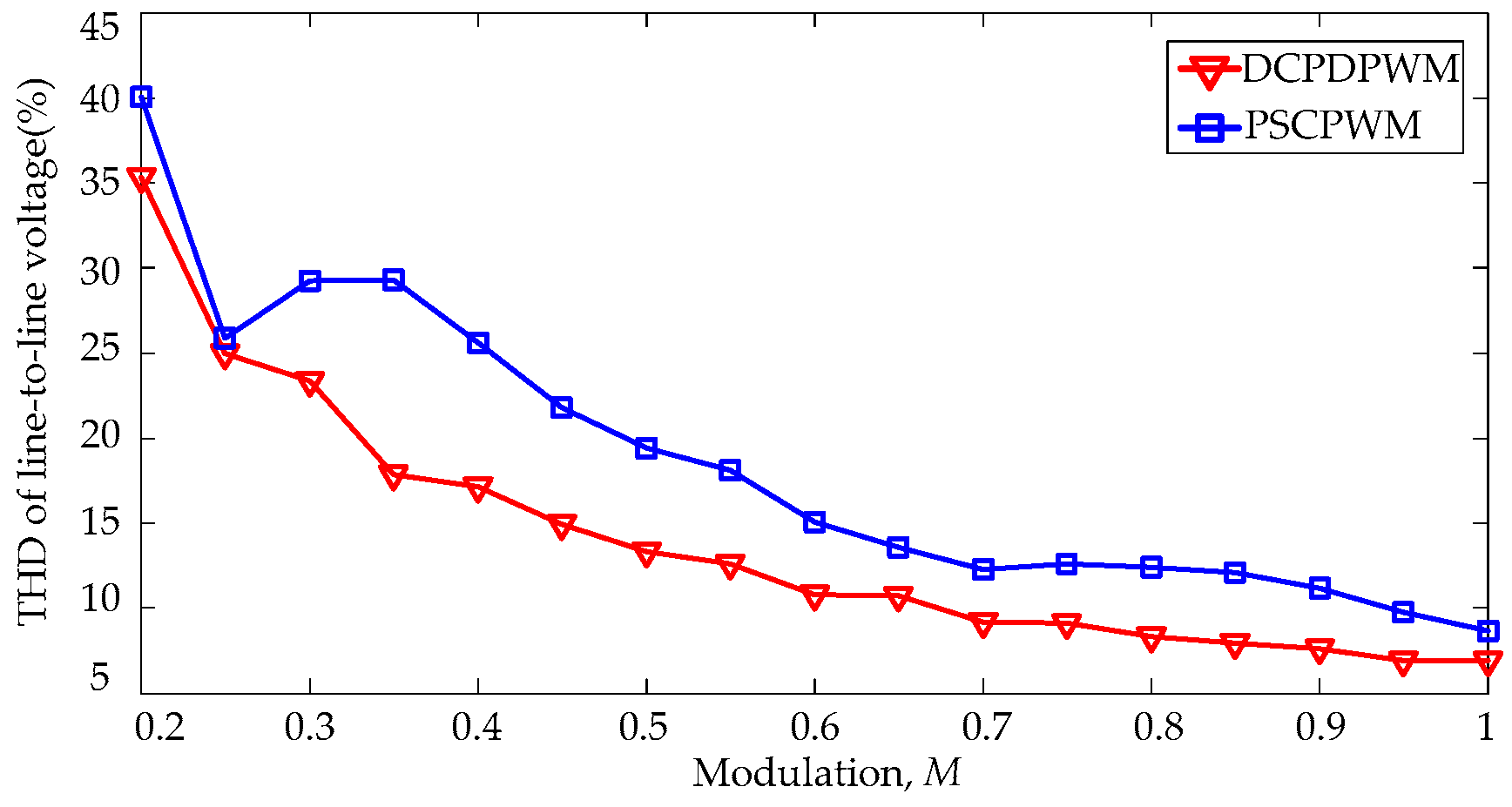
Comparison of the simulation results between the DCPDPWM and PSCPWM methods with circulating harmonics cancellation scheme are shown in Table 2. It can be seen that the total switching number per arm in 1 power grid period for PSCPWM and DCPDPWM are 80 and 79, respectively. The total harmonic distortion (THD) of line-to-line voltage and phase current for DCPDPWM are 6.89% and 3.91%, respectively. The THD of line-to-line voltage and phase current for PSCPWM are 9.77% and 7.01%, respectively. It is found that when the total switching frequency is basically the same, the DCPDPWM has better harmonic characteristics than PSCPWM with the circulating current harmonics cancellation scheme.
Figure 7 shows the THD of line-to-line voltage for DCPDPWM and PSCPWM for different modulation indexes with the circulating current harmonics cancellation scheme. It can be seen that DCPDPWM method has better line-to-line harmonic characteristics than the PSCPWM method in the whole modulation index region.
5.2. Comparison between DCPDPWM and PSCPWM Method with Output Voltage Harmonics Minimization Scheme
The comparison of simulation waveforms and harmonic spectra between the DCPDPWM and PSCPWM methods for MMC with output voltage harmonics minimization scheme are presented in Figure 8 and Figure 9, respectively.
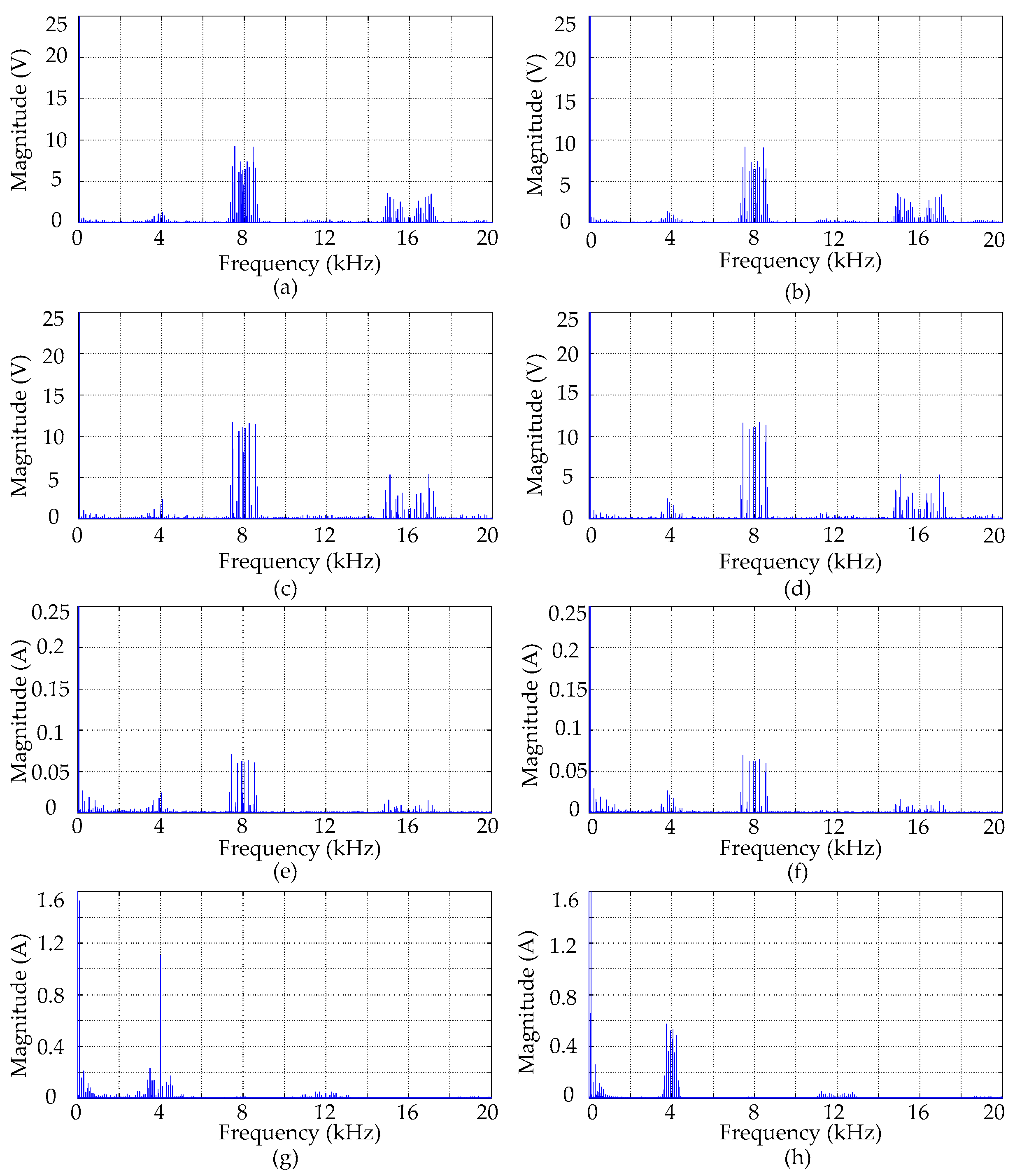
It can be seen that the voltage levels of phase voltage for both the PSCPWM and DCPDPWM methods rise to twenty-one. The equivalent switching frequency increases to fequ = 2fdcm = 2N × fpsc = 8000 Hz. It is found that the odd carrier harmonic components, and even sideband harmonic components of odd carrier groups in the phase voltage are completely eliminated in the line-to-line voltage for DCPDPWM, leaving only the even sideband harmonics of odd carrier groups. The sideband harmonic components of odd carrier groups in the phase voltage are cancelled for PSCPWM, leaving also the even sideband harmonics of odd carrier groups. It is found that the phase voltage, line-to-line voltage and phase current for PSCPWM and DCPDPWM methods have the same harmonic performance.
It can be seen that the harmonics of circulating currents between DCPDPWM and PSCPWM are different. The switching harmonics of circulating current for DCPDPWM includes odd carrier harmonic components and odd sideband harmonic components of even carrier groups. The main switching harmonics of DCPDWPM in the circulating current is the first carrier harmonic, while the switching harmonics of circulating current for PSCPWM consist of the sideband harmonics of carrier groups. It can be concluded that the simulation results completely agree with the theoretical analysis when applying the output voltage harmonics minimization scheme for DCPDPWM method.
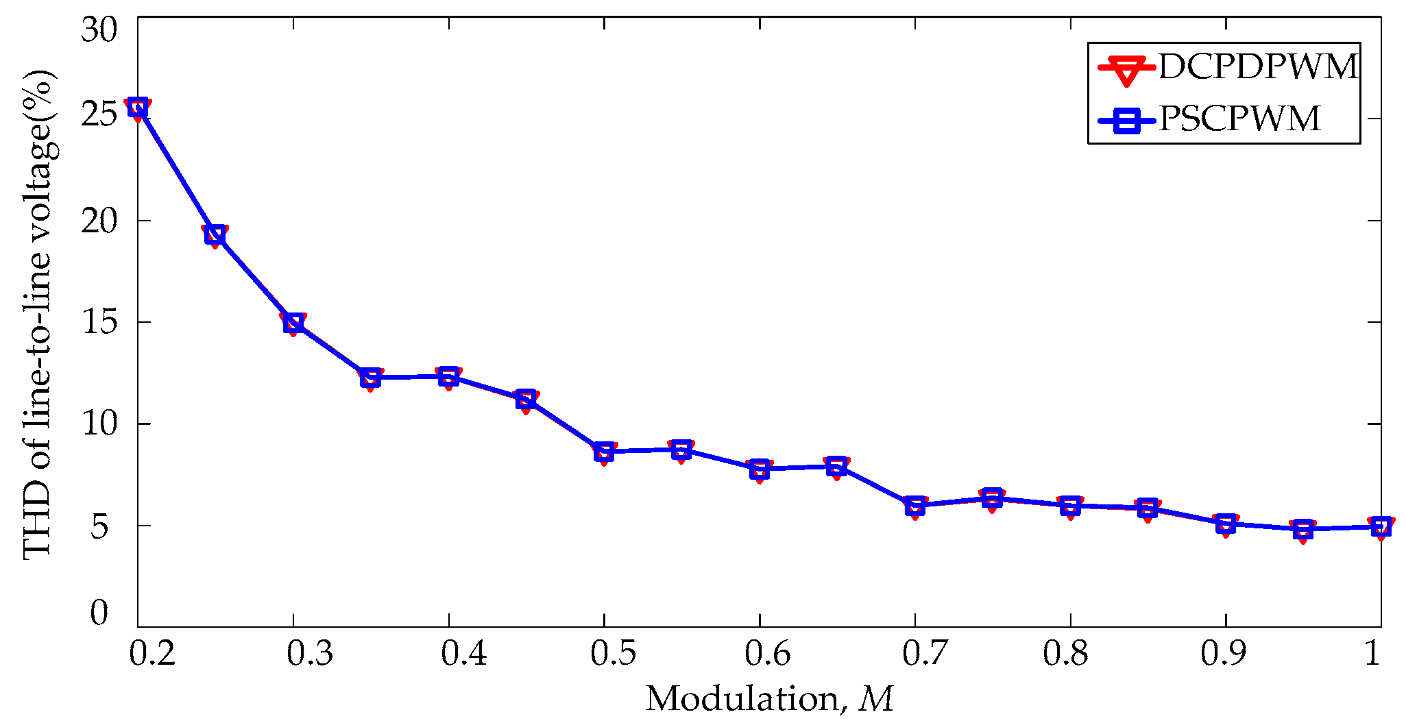
Comparison of simulation results between the DCPDPWM and PSCPWM methods with output voltage harmonics minimization scheme are shown in Table 3. It can be seen that when the total switching number per arm in 1 power grid period are basically the same, the THD of line-to-line output voltage and phase current for both the DCPDPWM and PSCPWM are 4.78% and 2.44%, respectively.
Figure 10 shows the THD of line-to-line voltage for DCPDPWM and PSCPWM methods in different modulation index with output voltage harmonics minimization scheme. It can be seen that DCPDPWM method has the same line-to-line voltage harmonic characteristics with PSCPWM method in the whole modulation index region.
6. Experimental Verification
In order to further verify the proposed method and theoretical analysis, a three-phase MMC laboratory prototype was built. The parameters of the prototype are shown in Table 4. The dc-link voltage is 400 V, and the number of SMs per arm is N = 4. A coupled inductor is adopted as the arm inductor, and a resistance-inductor load is used.
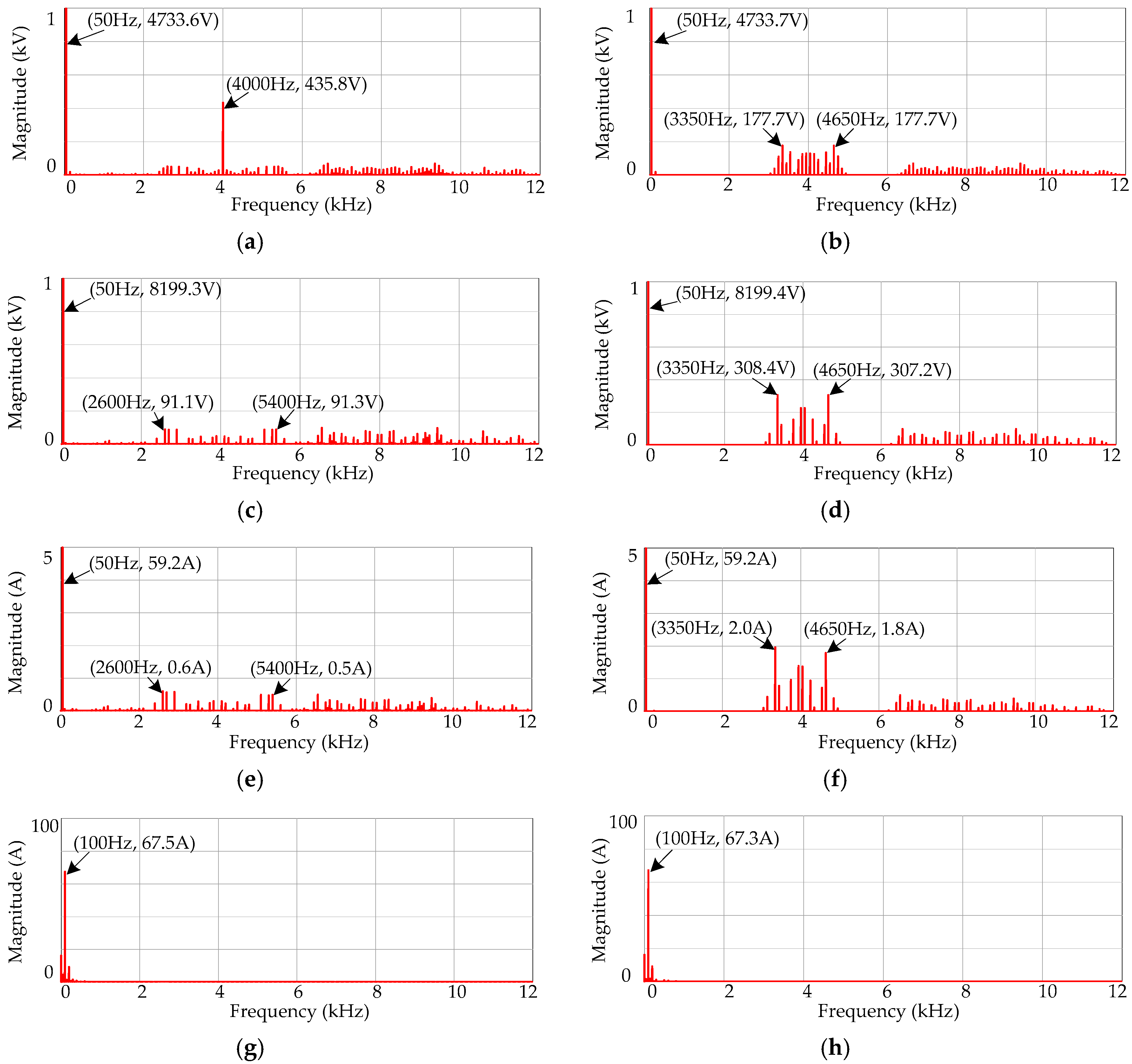
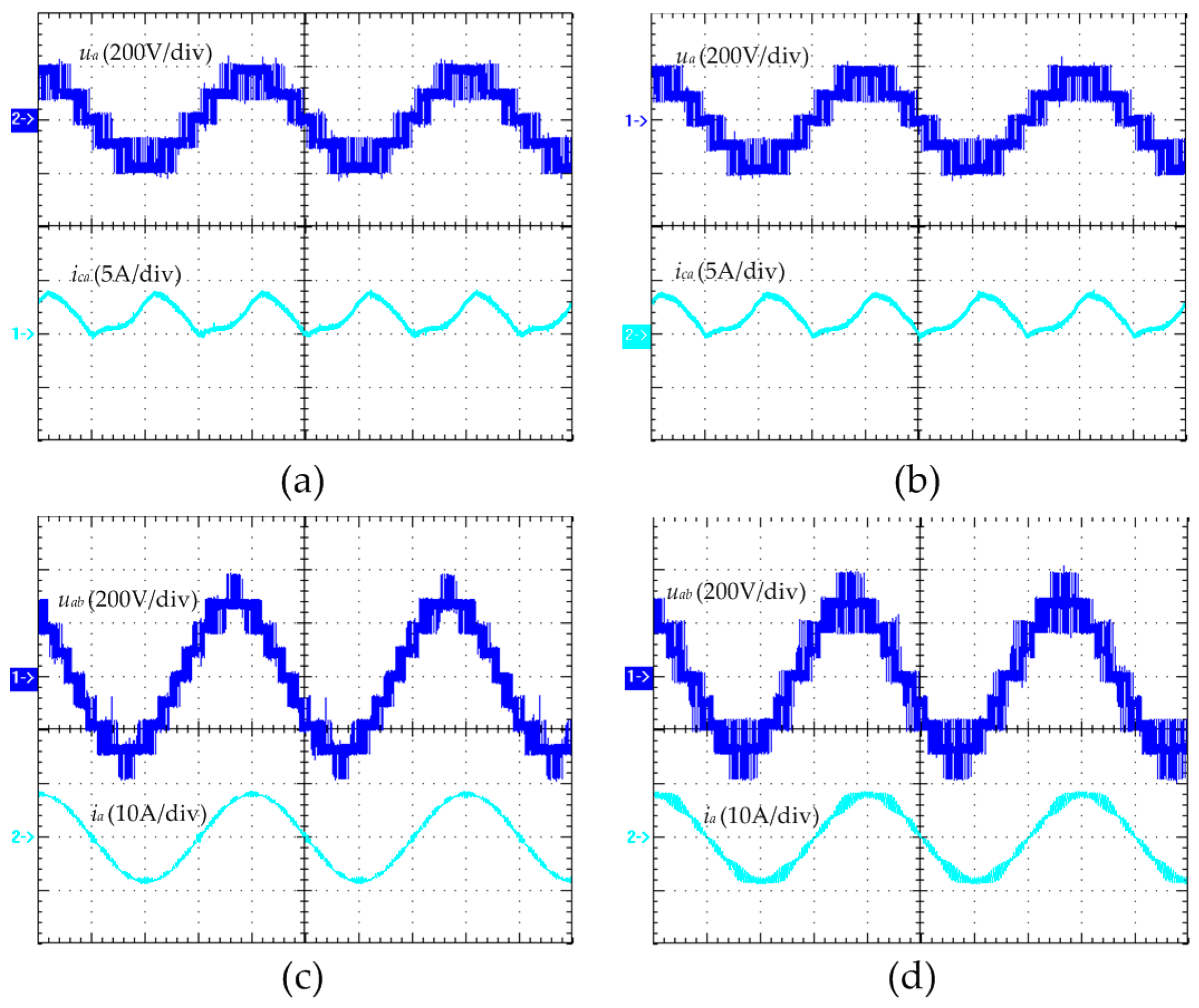
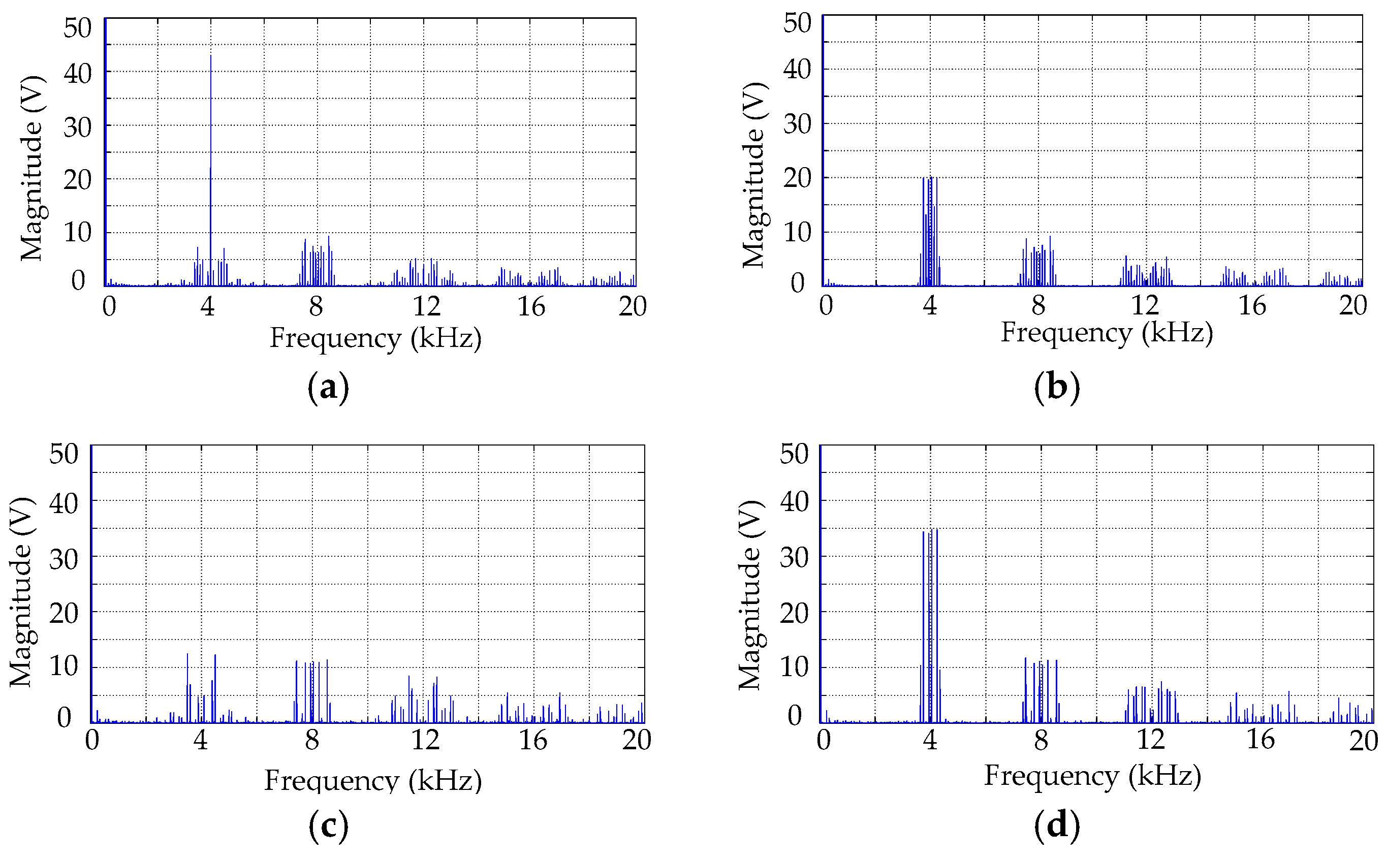
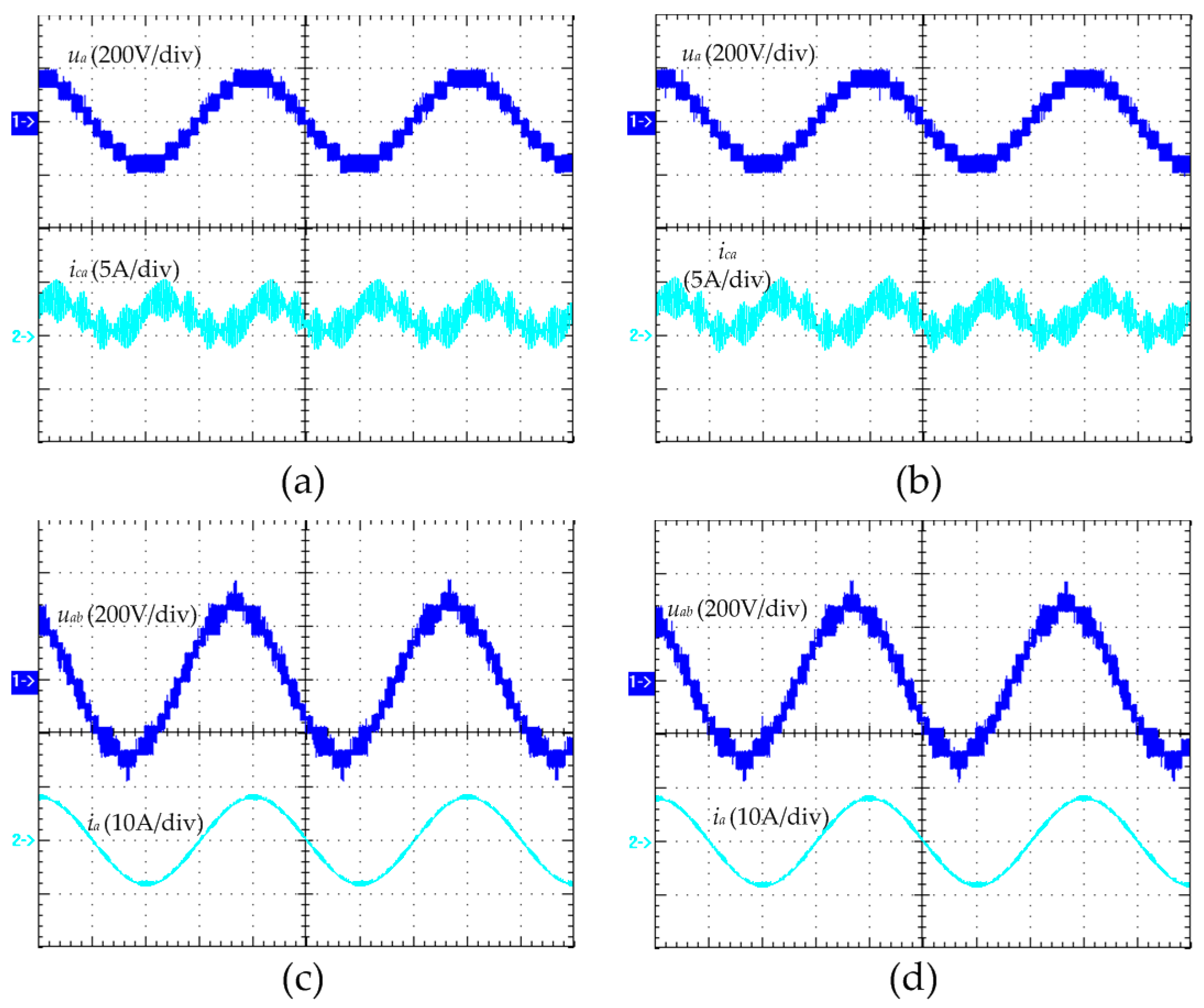
Figure 11 and Figure 12 show the experimental waveforms and harmonic spectra of DCPDPWM and PSCPWM with circulating current harmonics cancellation scheme, respectively. It is found that the switching harmonics of the circulating current are basically cancelled for DCPDPWM and PSCPWM methods. It can be seen that voltage level number of phase voltage is five, and the equivalent switching frequency of phase voltage for both the DCPDPWM and PSCPWM methods is 4000 Hz (fequ = fdcm = N × fpsc). For the DCPDPWM method, the main harmonic component of phase voltage is the first carrier harmonic component, which is eliminated in the line-to-line voltage. The harmonic components magnitudes in the line-to-line voltage and phase current for DCPDPWM are lower than PSCPWM with circulating current harmonics cancellation scheme.
From Figure 12, it can be seen that the THD of line-to-line voltage and phase current for DCPDPWM are 18.70% and 4.55%, respectively. The THD of line-to-line voltage and phase current for PSCPWM are 30.30% and 9.89%, respectively. The experimental results show that DCPDPWM has better harmonic characteristics than PSCPWM with the circulating current harmonics cancellation scheme. It is found that the experimental results match well with the theoretical analysis and simulation results.
Figure 13 and Figure 14 present the experimental waveforms and harmonic spectra of DCPDPWM and PSCPWM with output voltage harmonics minimization scheme, respectively. It can be seen that the voltage level number of the phase voltage increases to nine for both the DCPDPWM and PSCPWM methods, which means that the lower THD of phase voltage and line-to-line voltage can be achieved. It is found that the harmonic components of the first carrier groups are basically cancelled in the phase voltage, and the equivalent switching frequency of phase voltage for DCPDPWM and PSCPWM methods rises to 8000 Hz (fequ = 2 fdcm = 2 × N × fpsc).
Meanwhile, it can be seen that there are many switching harmonics in the circulating current, which causes high switching ripples in the waveform of circulating current. The circulating current harmonics for DCPDPWM are different with PSCPWM. The main switching harmonic component in the circulating current of DCPDPWM is the first carrier harmonic component, while the switching harmonics in the circulating current for PSCPWM are the sideband harmonic of the carrier groups. From Figure 14, it can be seen that the THD of line-to-line voltage and phase current for DCPDPWM are 13.27% and 2.93%, respectively. The THD of line-to-line voltage and phase current for PSCPWM are 13.34% and 2.98%, respectively. The experimental results show that DCPDPWM has the same harmonic characteristics than PSCPWM with the output voltage harmonics minimization scheme. The experimental results agree with the theoretical analysis and simulation results.
7. Conclusions
This paper has proposed a DCPDPWM method for MMCs. Only double triangular carriers with displacement angle are needed, one carrier for the lower arm, and the other carrier for the upper arm. The theoretical analysis of DCPDPWM for MMCs is presented by using a double Fourier integral analysis method. The Fourier series expression of phase voltage, line-to-line voltage and circulating current are deduced, and further the influence of carrier displacement angle between the upper and lower arms on the harmonic characteristics of the output voltage and circulating current is revealed. Furthermore, the optimum displacement angles are specified for the circulating current harmonics cancellation scheme and the output voltage harmonics minimization scheme. The proposed method and theoretical analysis are verified by simulations and experimental results.
It can be concluded that when applying the circulating current harmonics cancellation scheme, the carrier and associated sideband harmonics of the circulating current caused by DCPDPWM are completely cancelled, leaving only the dc component and low frequency components, which is similar to the circulating current harmonic characteristics for PSCPWM. The DCPDPWM method has better line-to-line voltage harmonic characteristics than the PSCPWM method with the same equivalent switching frequency. When applying the output voltage harmonics minimization scheme, the odd carrier harmonics and even sideband harmonics of odd carrier groups for phase voltage are eliminated, and the phase voltage and line-to-line voltage of DCPDPWM have the same harmonic characteristics as PSCPWM. However, the magnitudes of the odd carrier harmonics and odd sideband harmonics of even carrier groups for circulating current are at a maximum. The harmonic circulating current characteristics between the PSCPWM and DCPDPWM methods are different. The main harmonic caused by DCPDWPM in the circulating current is the first carrier harmonic, while the circulating current harmonics caused by PSCPWM consist of the carrier group sideband harmonics.
Acknowledgments
This work was supported by the National Natural Science Foundation of China (NSFC) under Grant No. 51477045.
Author Contributions
All the authors conceived and designed the study. Fayun Zhou performed the simulation and wrote the manuscript with guidance from An Luo and Yan Li. Fayun Zhou, Qianming Xu and Zhixing He performed the experiment. An Luo, Yan Li, Qianming Xu, Zhixing He and Josep M. Guerrero reviewed the manuscript and provided valuable suggestions.
Conflicts of Interest
The authors declare no conflict of interest.
Appendix A
The lower arm voltage can be obtained as:
where m denotes the carrier index variable and n refers to the baseband index variable.
The coefficients C0, C1, C2 are as follow:
where Jn(λ) represents the Bessel coefficient of order n and argument λ.
The upper arm voltage can be derived as:
Substituting (A1) and (A5) into (8), the phase voltage can be derived as:
References
- Lesnicar, A.; Marquardt, R. An innovative modular multilevel converter topology suitable for a wide power range. In Proceedings of the 2003 IEEE Bologna Power Tech Conference, Bologna, Italy, 23–26 June 2003. [Google Scholar]
- Marquardt, R. Modular multilevel converter: An universal concept for HVDC-networks and extended DC-bus-applications. In Proceedings of the 2010 International Power Electronics Conference, Sapporo, Japan, 21–24 June 2010. [Google Scholar]
- Akagi, H. Classification, terminology, and application of the modular multilevel cascade converter (MMCC). IEEE Trans. Power Electron. 2011, 26, 3119–3130. [Google Scholar] [CrossRef]
- Perez, M.A.; Bernet, S.; Rodriguez, J.; Kouro, S.; Lizana, R. Circuit topologies, modeling, control schemes, and applications of modular multilevel converters. IEEE Trans. Power Electron. 2015, 30, 4–17. [Google Scholar] [CrossRef]
- Debnath, S.; Qin, J.; Bahrani, B.; Saeedifard, M.; Barbosa, P. Operation, control, and applications of the modular multilevel converter: A review. IEEE Trans. Power Electron. 2015, 30, 37–53. [Google Scholar] [CrossRef]
- Nami, A.; Liang, J.; Dijkhuizen, F.; Demetriades, G.D. Modular multilevel converters for HVDC applications: Review on converter cells and functionalities. IEEE Trans. Power Electron. 2015, 30, 18–36. [Google Scholar] [CrossRef]
- Mohammadi, H.P.; Bina, M.T. A transformerless medium-voltage STATCOM topology based on extended modular multilevel converters. IEEE Trans. Power Electron. 2011, 26, 1534–1545. [Google Scholar]
- Zhuo, G.; Jiang, D.; Lian, X. Modular multilevel converter for unified power flow controller application. In Proceedings of the Third International Conference on Digital Manufacturing and Automation (ICDMA), Guilin, China, 31 July–2 August 2012. [Google Scholar]
- Shu, Z.; Liu, M.; Zhao, L.; Song, S.; Zhou, Q.; He, X. Predictive harmonic control and its optimal digital implementation for MMC-based active power filter. IEEE Trans. Ind. Electron. 2016, 63, 5244–5254. [Google Scholar] [CrossRef]
- Hagiwara, M.; Nishimura, K.; Akagi, H. A medium-voltage motor drive with a modular multilevel PWM inverter. IEEE Trans. Power Electron. 2010, 25, 1786–1799. [Google Scholar] [CrossRef]
- Liu, H.; Ma, K.; Poh, C.L.; Blaabjerg, F. Online fault identification based on an adaptive Observer for modular multilevel converters applied to wind power generation systems. Energies 2015, 8, 7140–7160. [Google Scholar] [CrossRef]
- Liu, H.; Ma, K.; Qin, Z.; Loh, P.C.; Blaabjerg, F. Lifetime estimation of MMC for offshore wind power HVDC application. IEEE J. Emerg. Sel. Topics Power Electron. 2016, 4, 504–511. [Google Scholar] [CrossRef]
- Mei, J.; Xiao, B.; Shen, K.; Tolbert, L.M.; Zheng, J.Y. Modular multilevel inverter with new modulation method and its application to photovoltaic grid-connected generator. IEEE Trans. Power Electron. 2013, 28, 5063–5073. [Google Scholar] [CrossRef]
- Trintis, I.; Munk-Nielsen, S.; Teodorescu, R. A new modular multilevel converter with integrated energy storage. In Proceedings of the IECON 2011–37th Annual Conference on IEEE Industrial Electronics Society, Melbourne, Australia, 7–10 November 2011. [Google Scholar]
- Konstantinou, G.; Pou, J.; Pagano, D.; Ceballos, S. A hybrid modular multilevel converter with partial embedded energy storage. Energies 2016, 9, 1012. [Google Scholar] [CrossRef]
- Jovcic, D.; Jamshidifar, A.A. Phasor model of modular multilevel converter with circulating current suppression control. IEEE Trans. Power Deliv. 2015, 30, 1889–1897. [Google Scholar] [CrossRef]
- Jamshidifar, A.; Jovcic, D. Small-signal dynamic DQ model of modular multilevel converter for system studies. IEEE Trans. Power Deliv. 2016, 31, 191–199. [Google Scholar] [CrossRef]
- Lu, X.; Lin, W.; Wen, J.; Yao, W.; An, T.; Li, Y. Dynamic phasor modelling and operating characteristic analysis of Half-bridge MMC. Proceedings of 2016 IEEE 8th International Power Electronics and Motion Control Conference (IPEMC-ECCE Asia), Hefei, China, 22–26 May 2016. [Google Scholar]
- Mehrasa, M.; Pouresmaeil, E.; Zabihi, S.; Catalao, J.P.S. Dynamic model, control and stability analysis of MMC-HVDC transmission systems. IEEE Trans. Power Deliv. 2016. [Google Scholar] [CrossRef]
- Wang, C.; Ooi, B.T. Incorporating deadbeat and low-frequency harmonic elimination in modular multilevel converters. IET Gener. Transm. Distrib. 2015, 9, 369–378. [Google Scholar] [CrossRef]
- Harnefors, L.; Antonopoulos, A.; Norrga, S.; Angquist, L.; Nee, H.P. Dynamic analysis of modular multilevel converters. IEEE Trans. Ind. Electron. 2013, 60, 2526–2537. [Google Scholar] [CrossRef]
- Darus, R.; Pou, J.; Konstantinou, G.; Ceballos, S.; Agelidis, V.G. Circulating current control and evaluation of carrier dispositions in modular multilevel converters. In Proceedings of the 2013 IEEE Energy Conversion Congress and Exhibition (ECCE Asia), Melbourne, Australia, 3–6 June 2013. [Google Scholar]
- Pou, J.; Ceballos, S.; Konstantinou, G.; Agelidis, V.G.; Picas, R.; Zaragoza, J. Circulating current injection methods based on instantaneous information for the modular multilevel converter. IEEE Trans. Ind. Electron. 2015, 62, 777–788. [Google Scholar] [CrossRef]
- Li, Y.; Jones, E.A.; Wang, F. Circulating current suppressing control’s impact on arm inductance selection for modular multilevel converter. IEEE J. Emerg. Sel. Topics Power Electron. 2017, 5, 182–188. [Google Scholar] [CrossRef]
- Leon, J.I.; Kouro, S.; Franquelo, L.G.; Rodriguez, J.; Wu, B. The essential role and the continuous evolution of modulation techniques for voltage-source inverters in the past, present, and future power electronics. IEEE Trans. Ind. Electron. 2016, 63, 2688–2701. [Google Scholar] [CrossRef]
- Konstantinou, G.; Pou, J.; Ceballos, S.; Darus, R.; Agelidis, V.G. Switching frequency analysis of staircase modulated modular multilevel converters and equivalent PWM techniques. IEEE Trans. Power Deliv. 2016, 31, 28–36. [Google Scholar] [CrossRef]
- Konstantinou, G.; Ciobotaru, M.; Agelidis, V.G. Selective harmonic elimination pulse-width modulation of modular multilevel converters. IET Power Electron. 2013, 6, 96–107. [Google Scholar] [CrossRef]
- Dahidah, M.S.A.; Konstantinou, G.; Agelidis, V.G. A review of multilevel selective harmonic elimination PWM: Formulations, solving algorithms, implementation and applications. IEEE Trans. Power Electron. 2015, 30, 4091–4106. [Google Scholar] [CrossRef]
- Ilves, K.; Antonopoulos, A.; Staffan, N.; Nee, H.P. A new modulation method for the modular multilevel converter allowing fundamental switching frequency. IEEE Trans. Power Electron. 2012, 27, 3482–3494. [Google Scholar] [CrossRef]
- Deng, Y.; Wang, Y.; Teo, K.H.; Harley, R.G. A simplified space vector modulation scheme for multilevel converters. IEEE Trans. Power Electron. 2016, 31, 1873–1886. [Google Scholar] [CrossRef]
- Tu, Q.; Xu, Z. Impact of sampling frequency on harmonic distortion for modular multilevel converter. IEEE Trans. Power Deliv. 2011, 26, 298–306. [Google Scholar] [CrossRef]
- Hu, P.; Jiang, D. A level-increased nearest level modulation method for modular multilevel converters. IEEE Trans. Power Electron. 2015, 30, 1836–1842. [Google Scholar] [CrossRef]
- Rohner, S.; Bernet, S.; Hiller, M.; Sommer, R. Modulation, losses, and semiconductor requirements of modular multilevel converters. IEEE Trans. Ind. Electron. 2010, 57, 2633–2642. [Google Scholar] [CrossRef]
- Li, Z.; Wang, P.; Zhu, H.; Chu, Z.; Li, Y. An improved pulse width modulation method for chopper-cell-based modular multilevel converters. IEEE Trans. Power Electron. 2012, 27, 3472–3481. [Google Scholar] [CrossRef]
- Hagiwara, M.; Akagi, H. Control and experiment of pulse width-modulated modular multilevel converters. IEEE Trans. Power Electron. 2009, 24, 1737–1746. [Google Scholar] [CrossRef]
- Lu, S.; Yuan, L.; Li, K.; Zhao, Z. An improved phase-shifted carrier modulation scheme for a hybrid Modular Multilevel Converter. IEEE Trans. Power Electron. 2017, 32, 81–97. [Google Scholar] [CrossRef]
- Saeedifard, M.; Iravani, R. Dynamic performance of a modular multilevel back-to-back HVDC system. IEEE Trans. Power Deliv. 2010, 25, 2903–2912. [Google Scholar] [CrossRef]
- Darus, R.; Konstantinou, G.; Pou, J.; Ceballos, S.; Agelidis, V.G. Comparison of phase-shifted and level-shifted PWM in the modular multilevel converter. In Proceedings of the International Power Electronics Conference (IPEC–ECCE Asia), Hiroshima, Japan, 18–21 May 2014. [Google Scholar]
- Mei, J.; Shen, K.; Xiao, B.; Tolbert, L.M.; Zheng, J. A new selective loop Bias mapping phase disposition PWM with dynamic voltage balance capability for modular multilevel converter. IEEE Trans. Ind. Electron. 2014, 61, 798–807. [Google Scholar] [CrossRef]
- Darus, R.; Pou, J.; Konstantinou, G.; Ceballos, S.; Picas, R.; Agelidis, V.G. A modified voltage balancing algorithm for the modular multilevel converter: Evaluation for staircase and phase-disposition PWM. IEEE Trans. Power Electron. 2015, 30, 4119–4127. [Google Scholar] [CrossRef]
- Fan, S.; Zhang, K.; Xiong, J.; Xue, Y. An improved control system for modular multilevel converters with new modulation strategy and voltage balancing control. IEEE Trans. Power Electron. 2015, 30, 358–371. [Google Scholar] [CrossRef]
- Ilves, K.; Antonopoulos, A.; Norrga, S.; Nee, H.P. Steady-state analysis of interaction between harmonic components of arm and line quantities of modular multilevel converters. IEEE Trans. Power Electron. 2012, 27, 57–68. [Google Scholar] [CrossRef]
- Li, B.; Yang, R.; Xu, D.; Wang, G.; Wang, W.; Xu, D. Analysis of the phase-shifted carrier modulation for modular multilevel converters. IEEE Trans. Power Electron. 2015, 30, 297–310. [Google Scholar] [CrossRef]
- Tu, Q.; Xu, Z.; Xu, L. Reduced switching-frequency modulation and circulating current suppression for Modular Multilevel Converters. IEEE Trans. Power Deliv. 2011, 26, 2009–2017. [Google Scholar]
- Holmes, D.G.; Lipo, T.A. Pulse Width Modulation for Power Converters: Principles and Practice; IEEE Press: Piscataway, NJ, USA, 2003. [Google Scholar]
- McGrath, B.P.; Holmes, D.G. An analytical technique for the determination of spectral components of multilevel carrier-based PWM methods. IEEE Trans. Power Deliv. 2002, 49, 847–857. [Google Scholar] [CrossRef]
- McGrath, B.P.; Holmes, D.G. Multicarrier PWM Strategies for Multilevel Inverters. IEEE Trans. Ind. Electron. 2002, 49, 858–867. [Google Scholar] [CrossRef]
Figure 1.
Schematic diagram of three phase modular multilevel converter (MMC). SM: sub-module.

Figure 2.
Principle of double-carrier phase-disposition pulse width modulation (DCPDPWM) for MMCs: (a) integer portion of the upper arm modulation signal; (b) integer portion of the lower arm modulation signal; (c) modulation of the remainder for the upper arm; (d) modulation of the remainder for the lower arm; (e) pulse width modulation (PWM) signal of the upper arm; (f) PWM signal of the lower arm; (g) number of on-state SMs for the upper arm; and (h) number of on-state SMs for the lower arm.

Figure 3.
Block diagram of double-carrier phase-disposition pulse width modulation for MMCs.

Figure 4.
Magnitudes of the harmonic components for the phase voltage and circulating current with different displacement angles: (a) magnitudes of harmonic components for phase voltage; and (b) magnitudes of harmonic components circulating current.
Figure 4.
Magnitudes of the harmonic components for the phase voltage and circulating current with different displacement angles: (a) magnitudes of harmonic components for phase voltage; and (b) magnitudes of harmonic components circulating current.

Figure 5.
Comparison of simulation waveforms between DCPDPWM and phase-shifted carrier pulse-width modulation (PSCPWM) methods with the circulating current harmonics cancellation scheme: (a) phase voltage of DCPDPWM; (b) phase voltage of PSCPWM; (c) line-to-line voltage of DCPDPWM; (d) line-to-line voltage of PSCPWM; (e) phase current of DCPDPWM; (f) phase current of PSCPWM; (g) circulating current of PDPWM; and (h) circulating current of PSCPWM.
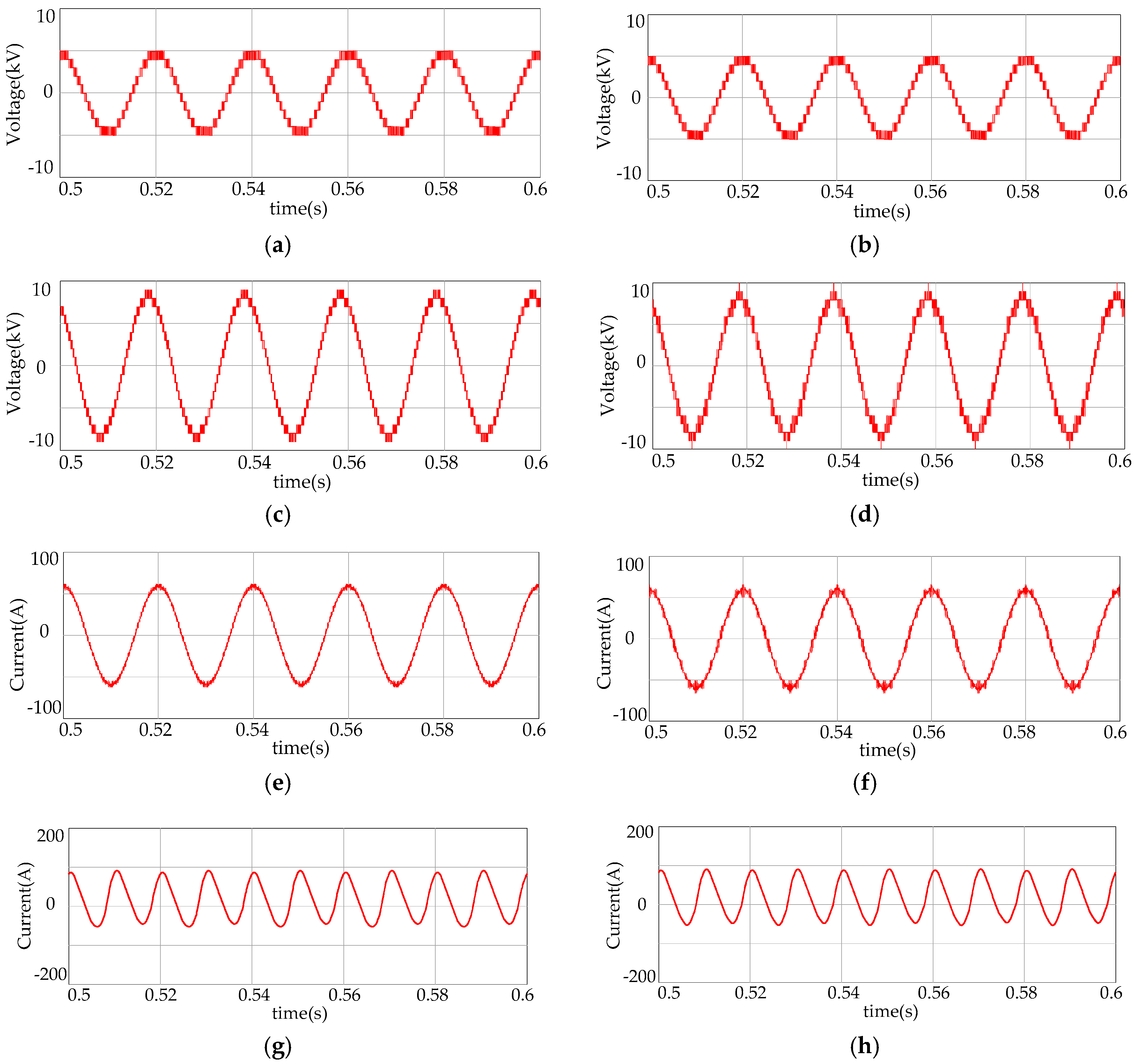
Figure 6.
Comparison of harmonic spectra between DCPDPWM and PSCPWM methods with the circulating current harmonics cancellation scheme: (a) phase voltage of DCPDPWM; (b) phase voltage of PSCPWM; (c) line-to-line voltage of DCPDPWM; (d) line-to-line voltage of PSCPWM; (e) phase current of DCPDPWM; (f) phase current of PSCPWM; (g) circulating current of PDPWM; and (h) circulating current of PSCPWM.

Figure 7.
THD of line-to-line voltage for DCPDPWM and PSCPWM methods in different modulation index with circulating current harmonics cancellation scheme.
Figure 7.
THD of line-to-line voltage for DCPDPWM and PSCPWM methods in different modulation index with circulating current harmonics cancellation scheme.

Figure 8.
Comparison of simulation waveforms between the DCPDPWM and PSCPWM methods with output voltage harmonics minimization scheme: (a) phase voltage of DCPDPWM; (b) phase voltage of PSCPWM; (c) line-to-line voltage of DCPDPWM; (d) line-to-line voltage of PSCPWM; (e) phase current of DCPDPWM; (f) phase current of PSCPWM; (g) circulating current of PDPWM; and (h) circulating current of PSCPWM.
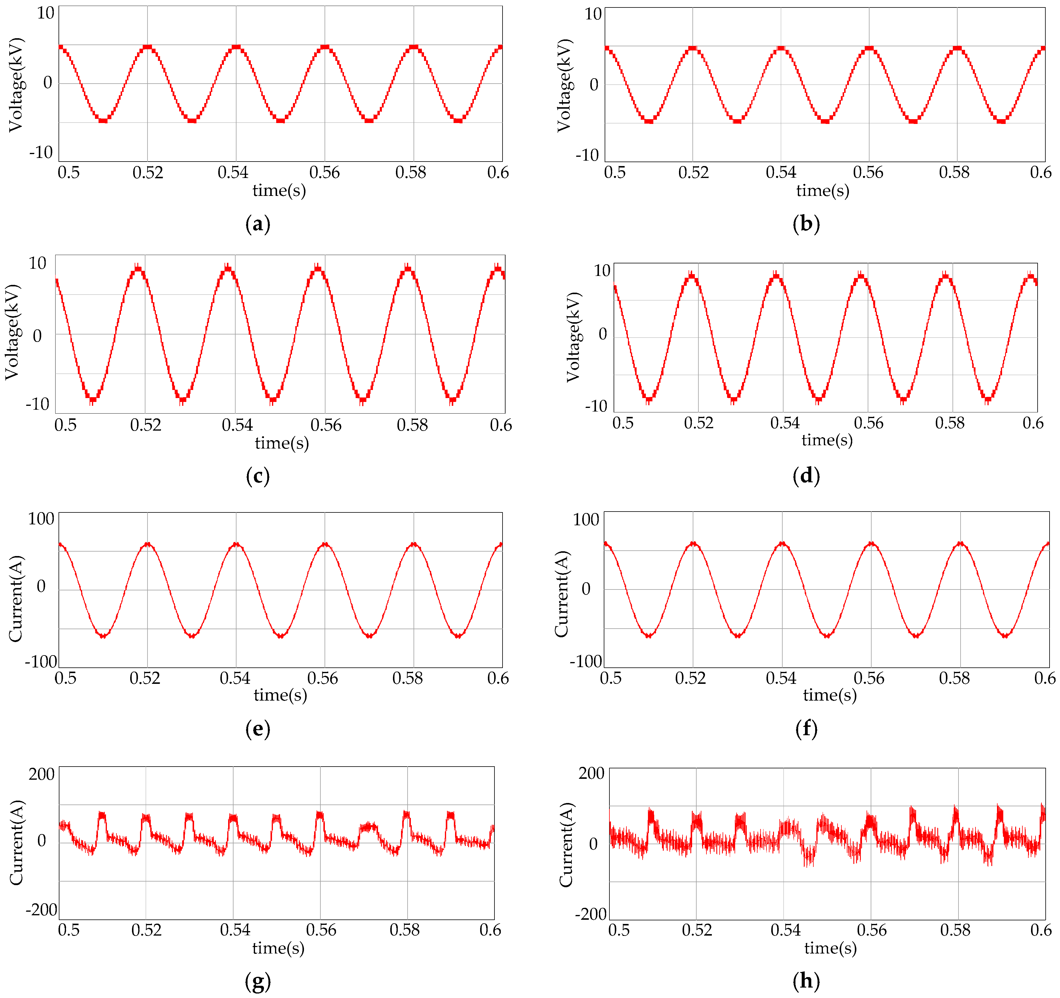
Figure 9.
Comparison of harmonic spectra between DCPDPWM and PSCPWM methods with output voltage harmonics minimization scheme: (a) phase voltage of DCPDPWM; (b) phase voltage of PSCPWM; (c) line-to-line voltage of DCPDPWM; (d) line-to-line voltage of PSCPWM; (e) phase current of DCPDPWM; (f) phase current of PSCPWM; (g) circulating current of PDPWM; (h) circulating current of PSCPWM.
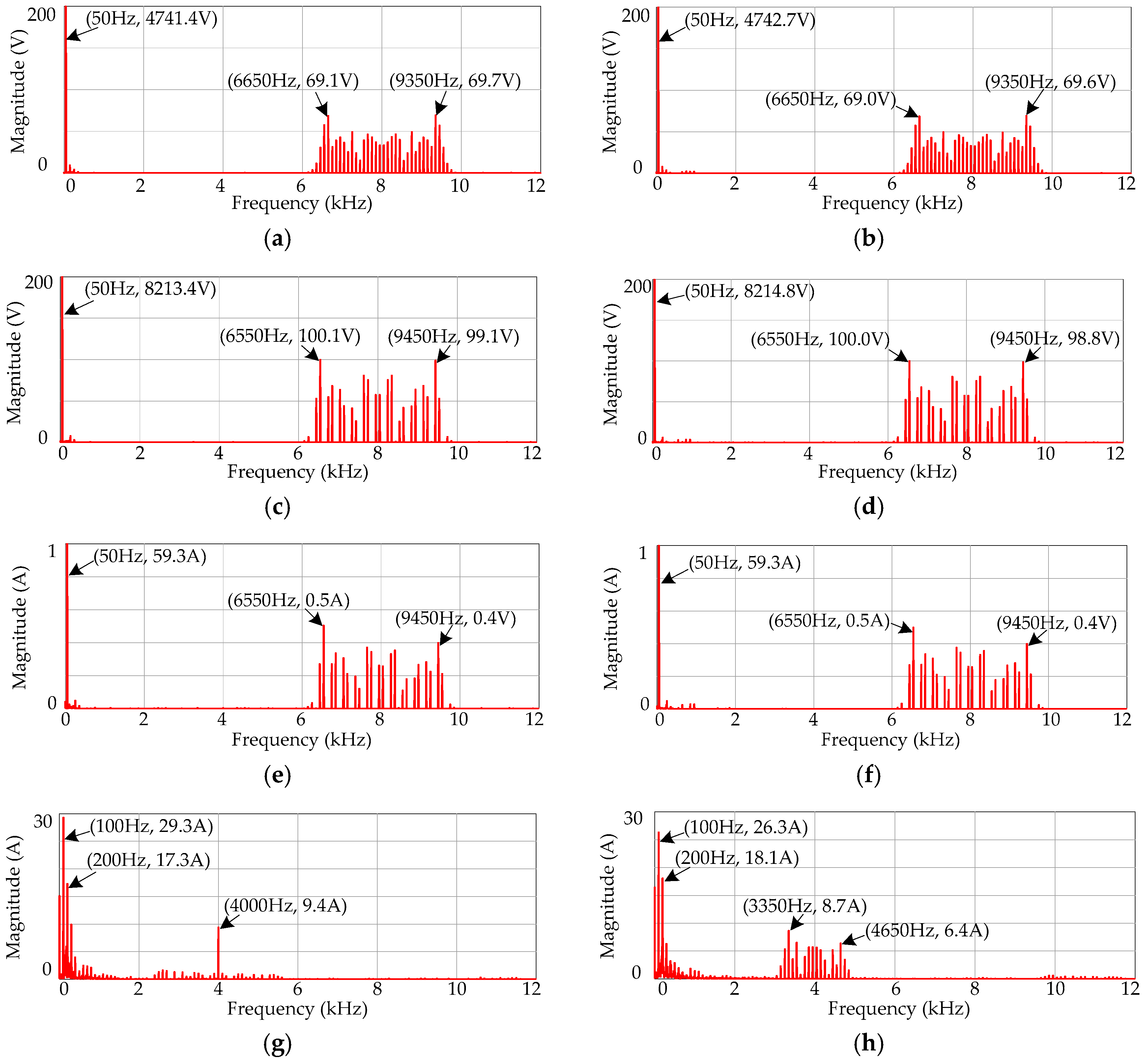
Figure 10.
THD of line-to-line output voltage for DCPDPWM and PSCPWM methods in different modulation index with output voltage harmonics minimization scheme.
Figure 10.
THD of line-to-line output voltage for DCPDPWM and PSCPWM methods in different modulation index with output voltage harmonics minimization scheme.

Figure 11.
Experimental waveforms of DCPDPWM method and PSCPWM method with circulating current harmonics cancellation scheme: (a) phase voltage and circulating current of DCPDPWM; (b) phase voltage and circulating current of PSCPWM; (c) line-to-line voltage and phase current of DCPDPWM; and (d) line-to-line voltage and phase current of PSCPWM.

Figure 12.
Harmonic spectra of experimental waveforms for the DCPDPWM and PSCPWM methods with circulating current harmonics cancellation scheme: (a) phase voltage of DCPDPWM; (b) phase voltage of PSCPWM; (c) line-to-line voltage of DCPDPWM; (d) line-to-line voltage of PSCPWM; (e) phase current of DCPDPWM; (f) phase current of PSCPWM; (g) circulating current of PDPWM; and (h) circulating current of PSCPWM.

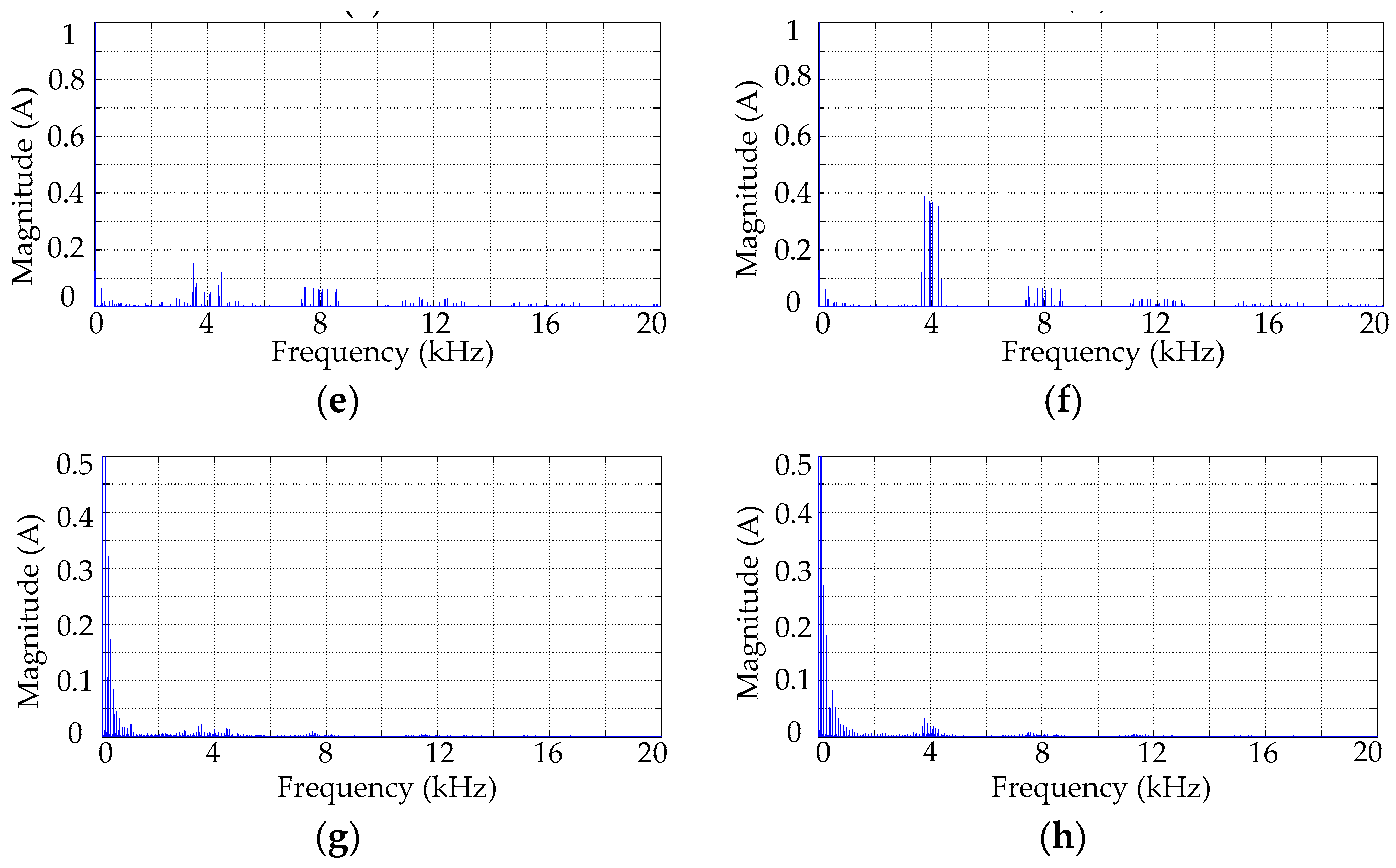
Figure 13.
Experimental waveforms of DCPDPWM method and PSCPWM method with output voltage harmonics minimization scheme: (a) phase voltage and circulating current of DCPDPWM; (b) phase voltage and circulating current of PSCPWM; (c) line-to-line voltage and phase current of DCPDPWM; (d) line-to-line voltage and phase current of PSCPWM.

Figure 14.
Harmonic spectra of experimental results for DCPDPWM and PSCPWM methods with output voltage harmonics minimization scheme: (a) phase voltage of DCPDPWM; (b) phase voltage of PSCPWM; (c) line-to-line voltage of DCPDPWM; (d) line-to-line voltage of PSCPWM; (e) phase current of DCPDPWM; (f) phase current of PSCPWM; (g) circulating current of PDPWM; and (h) circulating current of PSCPWM.


Table 1.
Parameters of the simulation.
| Parameter | Value |
|---|---|
| Number of SMs per arm | N = 10 |
| Frequency of reference voltage | fo = 50 Hz |
| Buffer inductors | Lp = Ln = Mu = 0.5 mH |
| Arm equivalent resistance | 0.1 Ω |
| SMs capacitance | C = 10 mF |
| DC-link voltage | Udc = 10000 V |
| Modulation index | M = 0.95 |
| Carrier frequency of DCPDPWM | fdcm = 4000 Hz |
| Carrier frequency of PSCPWM | fpsc = 400 Hz |
| Load inductance | Ld = 2 mH |
| Load resistance | Rd = 80 Ω |
Table 2.
Comparison of simulation results between DCPDPWM and PSCPWM methods with the circulating current harmonics cancellation scheme. THD: total harmonic distortion.
Table 2.
Comparison of simulation results between DCPDPWM and PSCPWM methods with the circulating current harmonics cancellation scheme. THD: total harmonic distortion.
| Modulation Methods | DCPDPWM | PSCPWM |
|---|---|---|
| THD of line-to-line output voltage (%) | 6.89 | 9.77 |
| THD of phase current (%) | 3.91 | 7.01 |
| Total switching number per arm (1 power grid period) | 79 | 80 |
Table 3.
Comparison of simulation results between DCPDPWM and PSCPWM method with the output voltage harmonics minimization scheme.
Table 3.
Comparison of simulation results between DCPDPWM and PSCPWM method with the output voltage harmonics minimization scheme.
| Modulation Methods | DCPDPWM | PSCPWM |
|---|---|---|
| THD of line-to-line output voltage (%) | 4.78 | 4.78 |
| THD of phase current (%) | 2.44 | 2.44 |
| Total number of switching per arm (1 power grid period) | 79 | 80 |
Table 4.
Parameters of Prototype.
| Parameter | Value |
|---|---|
| DC-link voltage | Udc = 400 V |
| Number of SMs per arm | N = 4 |
| Frequency of reference voltage | fo = 50 Hz |
| Arm inductor | Lp = Ln = Mu = 1 mH |
| SMs capacitance | C = 2.2 mF |
| Modulation index | M = 0.9 |
| Carrier frequency of DCPDPWM | fdcm = 4000 Hz |
| Carrier frequency of PSCPWM | fpsc = 1000 Hz |
| Load inductance | Ld = 2 mH |
| Load resistance | Rd = 20 Ω |
© 2017 by the authors. Licensee MDPI, Basel, Switzerland. This article is an open access article distributed under the terms and conditions of the Creative Commons Attribution (CC BY) license (http://creativecommons.org/licenses/by/4.0/).
Share and Cite
MDPI and ACS Style
Zhou, F.; Luo, A.; Li, Y.; Xu, Q.; He, Z.; Guerrero, J.M. Double-Carrier Phase-Disposition Pulse Width Modulation Method for Modular Multilevel Converters. Energies 2017, 10, 581. https://doi.org/10.3390/en10040581
AMA Style
Zhou F, Luo A, Li Y, Xu Q, He Z, Guerrero JM. Double-Carrier Phase-Disposition Pulse Width Modulation Method for Modular Multilevel Converters. Energies. 2017; 10(4):581. https://doi.org/10.3390/en10040581
Chicago/Turabian StyleZhou, Fayun, An Luo, Yan Li, Qianming Xu, Zhixing He, and Josep M. Guerrero. 2017. "Double-Carrier Phase-Disposition Pulse Width Modulation Method for Modular Multilevel Converters" Energies 10, no. 4: 581. https://doi.org/10.3390/en10040581
Note that from the first issue of 2016, this journal uses article numbers instead of page numbers. See further details here.