
A Modular Multilevel Converter with Power Mismatch Control for Grid-Connected Photovoltaic Systems
by
Turgay Duman
*, 
Shilpa Marti
,
M. A. Moonem
,
Azas Ahmed Rifath Abdul Kader
and
Hariharan Krishnaswami
Department of Electrical and Computer Engineering, The University of Texas at San Antonio, One UTSA Circle, San Antonio, TX 78249, USA
*
Author to whom correspondence should be addressed.
Energies 2017, 10(5), 698; https://doi.org/10.3390/en10050698
Submission received: 30 January 2017
/
Revised: 10 May 2017
/
Accepted: 12 May 2017
/
Published: 17 May 2017
(This article belongs to the Section F: Electrical Engineering)
Abstract
:A modular multilevel power converter configuration for grid connected photovoltaic (PV) systems is proposed. The converter configuration replaces the conventional bulky line frequency transformer with several high frequency transformers, potentially reducing the balance of systems cost of PV systems. The front-end converter for each port is a neutral-point diode clamped (NPC) multi-level dc-dc dual-active bridge (ML-DAB) which allows maximum power point tracking (MPPT). The integrated high frequency transformer provides the galvanic isolation between the PV and grid side and also steps up the low dc voltage from PV source. Following the ML-DAB stage, in each port, is a NPC inverter. N number of NPC inverters’ outputs are cascaded to attain the per-phase line-to-neutral voltage to connect directly to the distribution grid (i.e., 13.8 kV). The cascaded NPC (CNPC) inverters have the inherent advantage of using lower rated devices, smaller filters and low total harmonic distortion required for PV grid interconnection. The proposed converter system is modular, scalable, and serviceable with zero downtime with lower foot print and lower overall cost. A novel voltage balance control at each module based on power mismatch among N-ports, have been presented and verified in simulation. Analysis and simulation results are presented for the N-port converter. The converter performance has also been verified on a hardware prototype.
1. Introduction
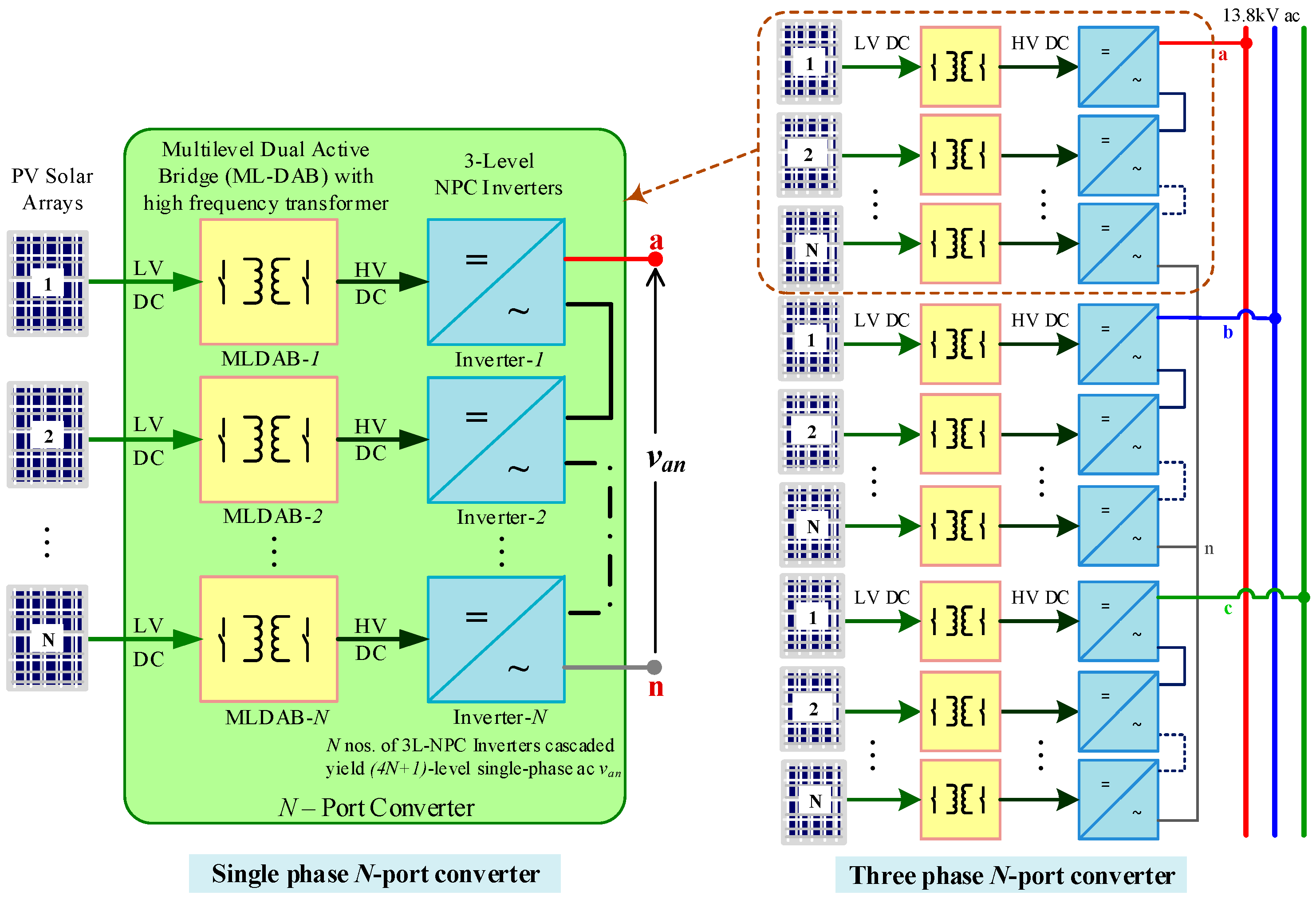
Grid-connected large-scale photovoltaic (PV) systems have to consider challenges such as energy yield, power conversion efficiency, power density, reliability and cost which includes solar panels, power electronics and balance of systems (BOS) cost. Utility scale PV plants use single or multiple centralized inverters rated from 500 kW or higher to output power at a three phase voltage level of 480 V or less. Some megawatt (MW) scale PV inverters are designed for a higher input dc voltages such as 2500 V [1] in order to reduce the dc BOS cost and increase efficiency up to 99.5% [1,2]. Large PV plants still rely on line frequency (i.e., 50 or 60 Hz) transformers because of its high efficiency to isolate and step-up the inverter’s output voltage to the distribution voltage level of 11 to 13 kV for interconnection with the utility grid. In the MW power range, transformer cost is more than one-third of the inverter cost and occupies close to one-third of the footprint of a 1 MW inverter station. A price comparison has been shown in a report prepared by the U.S. Idaho National Laboratory in May 2012 [3] and these prices may vary widely depending on market fluctuations, manufacturer, windings material, features, etc. The average cost of a 500 kVA GE transformer operating at 60% load with a power factor of 0.85 is 11.92 ¢/watt for 99% efficiency [3]. The total cost including transportation, installation, other transformer related balance of system costs and regular maintenance cost make this ¢/watt estimate more than twice of the transformer price. A 500 kVA 12 kV/400 V 60 Hz transformer weighs roughly 1~2.5 tons based on the type and manufacturing material which is a concern for transportation and installation. The proposed N-port converter uses smaller and lightweight medium frequency transformers integrated within the dc-dc converter at each identical port.
Research has been going on to eliminate the bulky line frequency transformers at the grid interface using different converter topologies and configurations [4,5,6,7,8]. Various topologies, standards and evolution of PV converters are reviewed in literature [4,9,10]. Optimum choice in topology, components and operating parameters can increase energy injected into the grid by 9–15% and lowering the levelized cost of energy (LCOE) up to 17% for grid connected PV system [11]. One of the major challenges in achieving medium or high voltage in a PV converter is the limitation of switching device (i.e., IGBT, Diode) and associated components’ voltage handling capability. A 15 kV silicon-carbide (SiC) switching device performance is reported in [12] and up to 6.5 kV IGBTs are commercially available. Multilevel topologies can overcome shortcomings in solid-state switching device ratings so that they can be applied to higher voltage systems, and additionally they provide low total harmonic distortion (THD) and lower dv/dt. Commonly used multilevel topologies are neutral point clamped (NPC), flying capacitor (FC) and cascaded H-bridge (CHB). NPC topology is an effective way to eliminate the leakage current for transformer-less PV inverters [13]. CHB offers the flexibility in choosing the number of modules to be cascaded based on the voltage and power requirement. In the proposed topology N-nos. of phase-shifted NPC inverters are cascaded at the output of each port to yield the desired voltage level. This cascaded NPC (CNPC) topology provides (4N + 1) levels at the cascaded output voltage where the CHB provides (2N + 1) levels for N cascaded ports which is advantageous in terms for lower dv/dt and lower device voltage ratings in comparison to the CHB topology.
Modular multilevel converter (MMC or M2LC or M2C) topology has been proposed in [14] and it is used in a 26.5 kV 36 MW grid intertie system. For PV applications modularity at the input side with two stage power conversion is advantageous as shown in a study on a commercially available large-scale PV inverter that replaces the PV side dc combiners with dc-dc converters at string-level along with maximum power point tracking (MPPT) which increases the energy yield by 34–46% in comparison to a single central inverter for certain shading conditions [15]. A multilevel-multistring configuration with CHB topology has been proposed in [16] which increases the PV system capacity and improves the power quality. A 3 MW 12 kV modular CHB for grid-connected PV system is proposed in [17] where the dc-dc conversion stage is a two-level dual active bridge (DAB) and multiple of such dc outputs are added to feed an inverter module in the cascade. In [18] a common high-frequency link transformer is used to isolate the cascaded inverter modules which also minimizes the voltage imbalance and common mode issue. A multi-port multi-level topology for PV application has been proposed in [8] where the dc-ac stage uses four-quadrant switches instead of dc-dc and dc-ac conversion stages. In terms of the number of semiconductor switches used in dc-ac converter, this is the same as separate dc-dc and dc-ac converters. In [19,20], 15 kV SiC IGBTs have been used instead of cascading to reach higher voltages. The high voltage, however, poses several challenges in handling high dv/dt parasitic at high frequencies and THD requirement for PV-grid interconnection. A high-frequency-link based grid-tied PV system is proposed in [21]. The innovations are in the small dc bus link capacitor thereby improving the reliability of the system by replacing electrolytic capacitors with film capacitors. Capacitor voltage unbalance among different modules is a common issue for CHB inverter topology. Various control algorithms have been discussed in literature to address these voltage and power balancing issues [17,22,23,24,25].
The state-of-the art utility scale PV power converters continue to address size and cost challenges through modularity and innovative. Specifically, in this paper an N-port power electronic converter architecture with integrated high-frequency transformer is presented, which eliminates the line frequency transformer and reduces the overall cost for grid-connected PV plants. The proposed architecture is modular from the PV source up to the grid before cascading and each module consists of a dc-dc and a dc-ac power conversion stage. MPPT control is decoupled from the voltage and power balance control. MPPT is performed at the front end dc-dc multilevel DAB (ML-DAB) stage using the phase-shift control. The ML-DAB also independently controls any voltage mismatch between two clamping capacitors used in the NPC bridge as the dc-link. This ML-DAB not only provides isolation between PV and grid side, it also boosts up the PV side dc voltage for the next inverter stage. The proposed dc-dc three-level NPC DAB stage allows one to synthesize the same number of voltage levels at the high voltage bridge of ML-DAB that can be produced using two cascaded two-level conventional DABs, so the ML-DAB is saving one high frequency transformer in comparison with two cascaded H-bridges while performing the same voltage step-up operation similar to two CHBs. The N-port converter allows for a direct medium-voltage (e.g., 13.8 kV) interconnection without the need of a bulky line frequency transformer. Modularity provides serviceability with zero downtime. Presented design is also highly scalable. Despite medium to high voltages, the converter can be realized by lower voltage rated devices. Due to the cascaded multilevel configuration at the ac output stage, the N-port converter has the inherent advantage of low THD required for PV grid interconnection. The building blocks of the proposed N-port converter are shown in Section 2. A study on cost-effectiveness of proposed N-port in comparison to a standard 1 MW PV power system having central inverter has also been shown in Section 2. MPPT, voltage balancing control of clamping capacitors at the inverter input and power mismatch control among different ports are described in Section 3. Section 4 consists of simulation and experimental results.
2. Proposed N-Port Converter Architecture
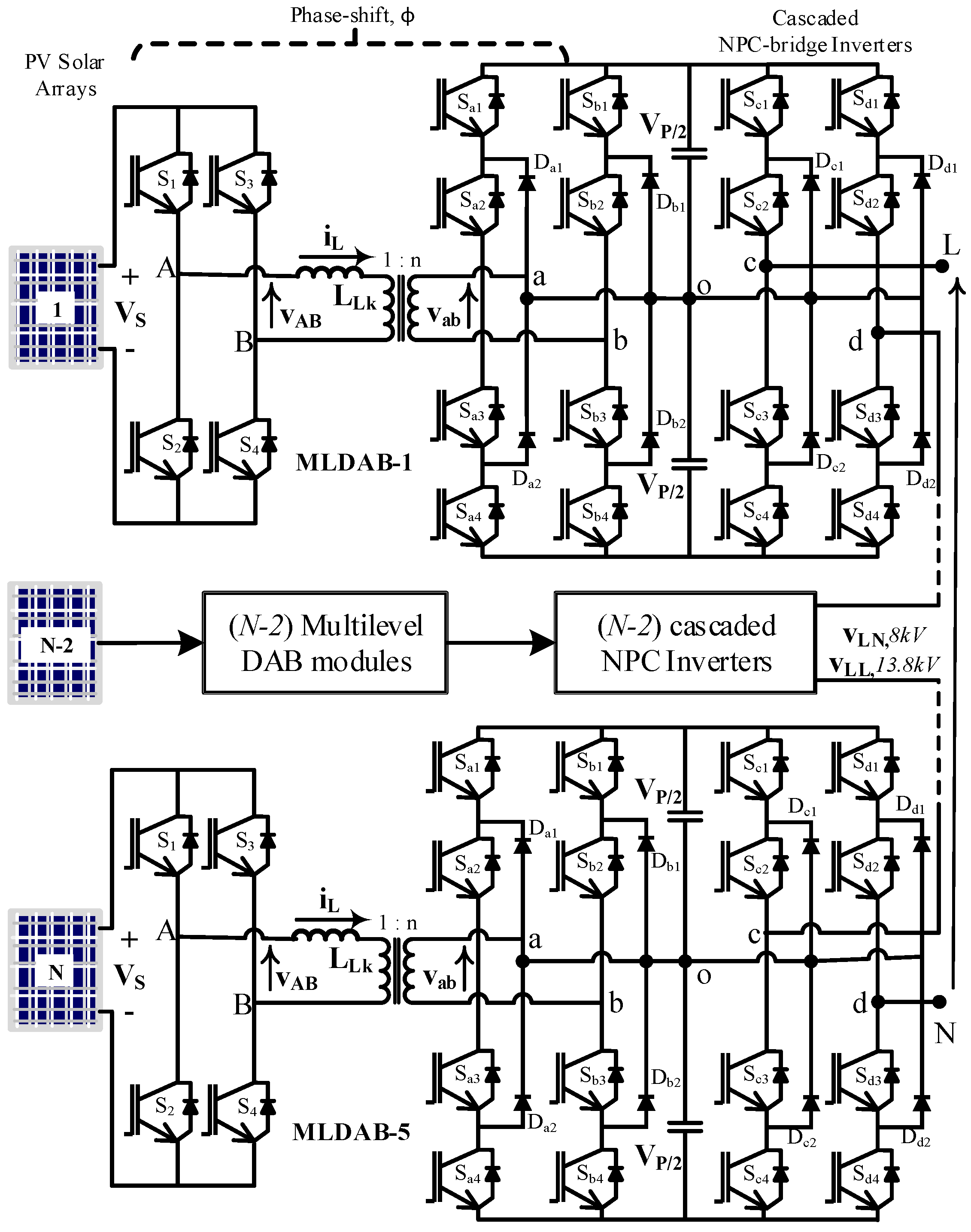
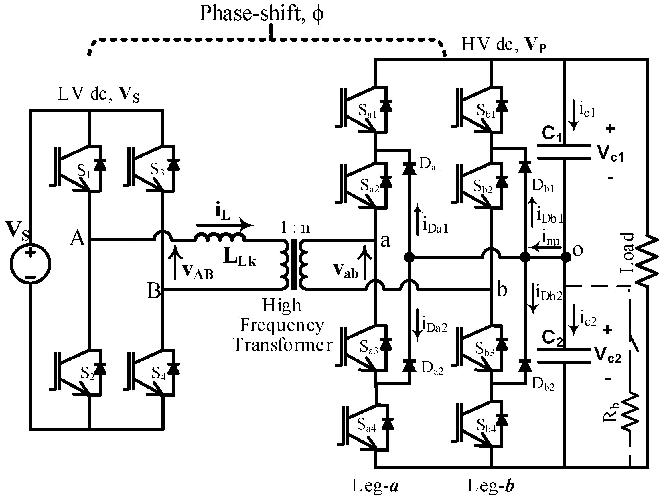
The proposed N-port converter architecture is shown in Figure 1. The N-port converter consists of N numbers of modular dc-dc and dc-ac power conversion stages in between PV and grid interface. Each port includes a dc-dc multilevel dual active bridge (ML-DAB) converter followed by a NPC inverter. The high voltage bridge of the dc-dc ML-DAB has a three-level NPC configuration which is connected in a back-to-back manner with the NPC inverter having the common neutral point “o” as shown in Figure 2. The PV dc voltage is stepped up in two stages, first in the dc-dc ML-DAB stage and then in the NPC inverter stage by cascading which yields the overall voltage up to 13.8 kV three-phase line-to-line rms. Each ML-DAB supplies a three-level NPC-bridge inverter and all the N inverters are cascaded to produce a single-phase line-to-neutral voltage of 7.96 kV (Figure 2). The following sub-sections describe the building blocks of this N-port converter in detail.
2.1. dc-dc Power Conversion Stage
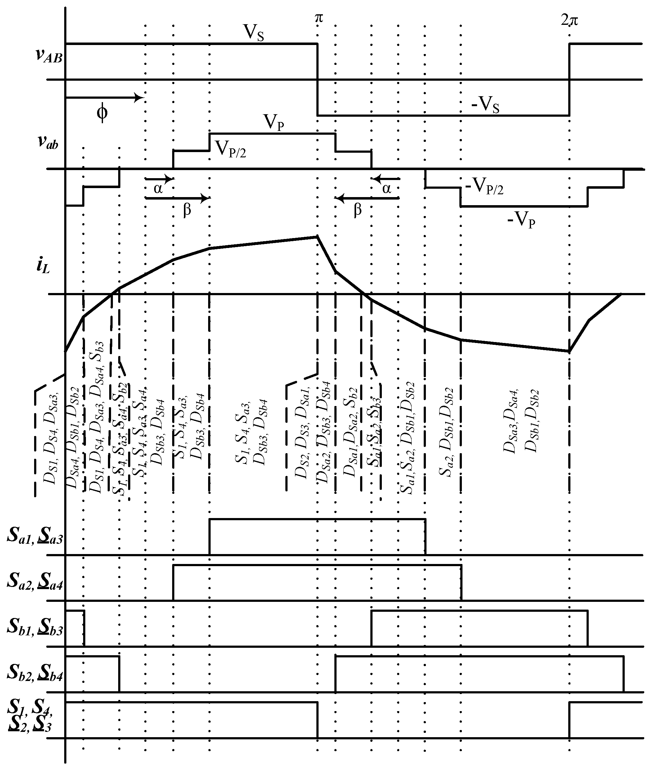
Various transformer-less and transformer-isolated dc-dc power conversion topologies have been proposed for grid-connected PV applications [4,16,26]. In the proposed topology, ML-DAB is the first power conversion stage that boosts up the dc voltage obtained from the PV array and also provides isolation between PV and the grid. The concept of DAB was initially proposed in [27]. Since then DAB is being used for transformer isolated dc-dc conversion in medium and high power applications. In the conventional two-level DAB, two active bridges across a high frequency transformer produce two square waves which are phase-shifted to control the power flow. On the advances in DAB, [28] proposes a semi-dual active bridge (S-DAB) dc-dc converter for unidirectional power flow (e.g., PV application) where the load-side bridge has two switches and two diodes instead of four active switches used in conventional DAB. Operating principle and characteristic advantages are similar to conventional DAB but the S-DAB lacks a multilevel topology (e.g., a NPC stage) suitable for medium or high-voltage applications. The proposed ML-DAB topology for the N-port converter (Figure 2.) consists of the PV side primary bridge (switches S1 to S4) which produces a two-level square wave vAB and the secondary bridge which is composed of two 3-level (3L) neutral point clamped (NPC) legs produces a leg-to-leg 5-level (5L) VAB staircase waveform as shown in Figure 3. Conventionally, NPC legs are used in multi-level inverter applications. In the proposed ML-DAB application, each of the switches in the NPC bridge (Sa1 to Sa4 and Sb1 to Sb4) is subjected to a maximum voltage stress of Vp/2 while the five-level voltage Vab across the transformer has maximum peak voltage Vp.
In order to synthesize the 5L voltage vab, switching pulses and resulting voltage waveforms are defined with respect to angular distances (i.e., α,β) instead of the duty cycle. These angles α,β are measured symmetrically at zero, π and 2π within a switching period (Figure 3). The zero and π are considered at the mid-point of the zero voltage level of the 5L voltage vab. Defining vab in such a symmetrical way is advantageous in terms of the minimum number of parameters (α, β) required. This provides a straightforward method for derivation of a simple mathematical expression for power flow in the ML-DAB [29]. Parameters α and β shape the multilevel voltage waveform and are used in voltage balancing of the clamping capacitors. The phase-shift angle φ is independent of α, β and acts as the control parameter to control the power flow in the ML-DAB.
The novelty of such an NPC based ML-DAB is that it can handle a higher output dc voltage (Vp) due to the multilevel topology which reduces both the voltage stress on switches and the dv/dt. The 5L voltage waveform (vab) across the high frequency transformer also reduces the THD in comparison to conventional 2L DAB. On the other hand, a higher dc voltage (Vp) is achieved in one ML-DAB module (1-port in Figure 2) using one single-phase transformer, whereas doing the same with two cascaded 2L DABs would require at least two high-frequency transformers and more semiconductor switches.
2.1.1. Power Flow through the dc-dc ML-DAB
Power flow from the PV dc bus to the high voltage dc bus is based on the phase-shift between two active bridges. The phase-shift φ is defined based on the phase difference between the fundamental of the primary side 2L vab and NPC bridge output 5L vab as shown in Figure 3.
In this topology, 3L NPC diode clamped legs form the high voltage side multilevel (5L) bridge. Sector-wise inductor current () at all different switching transitions has been analyzed in terms of
and in order to find the power-flow expression. From the fundamental relation of inductor voltage and current we get:
Here, current through transformer’s leakage inductance:
Now writing this equation for each segment of from 0 to and equating as shown in Figure 3 we get:
The average power flow equation from primary bridge to secondary bridge through the leakage inductance can be written as follows:
Putting the expression of in at different segment (Figure 3) we get the power flow equation for the condition of as:
In the above Equations (5) and (6), is the transferred power through the high frequency transformer, is the PV side dc voltage, is the inverter side dc voltage, where is the switching frequency, is the transformer turns ratio, is the voltage conversion ratio defined as and is the primary referred leakage inductance used at the high frequency link.
2.1.2. Soft-Switching Operation of ML-DAB
The conventional two level DAB topology can achieve zero voltage switching (ZVS) for all switches in the entire power range when is equal to unity. The switching pulses for the 2 L-to-5 L DAB switches are shown in Figure 3. It is possible to achieve the same in the primary bridge ( to with the condition of . ZVS happens in the switches of the NPC bridge during turn-on at . The rest of the switches are also turned on when the current through the switch is already zero. and are to be turned-on at ZVS when and are to be turned-on at ZVS when In order to avoid the short circuit condition between (7) and (8) zero crossing of should be avoided in the following regions:
By choosing an optimum range of ZVS turn-ON can be achieved in eight out of twelve switches. The above analysis of soft-switching operation in ML-DAB becomes important if the IGBTs are replaced by SiC Mosfets operating at higher switching frequencies. Recent development in silicon carbide (SiC) Mosfets, at the voltage level of 1200 V or higher, offer significantly lower switching loss—as much as 90% compared with silicon IGBTs, due to the absence of tail current and fast recovery characteristics of the body diode [30]. Using SiC based switching devices the switching frequency can be in the order of hundred kHz, which in turn reduces the size of reactive components used in the converter.
2.1.3. Transformer Design
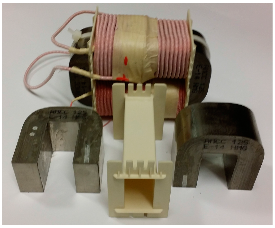
The medium/high frequency transformer is used within the dc-dc ML-DAB stage which isolates the PV side from the grid. The transformer frequency is essentially same as the switching frequency used for the 12 switches used in the primary and secondary bridges in the ML-DAB. Higher switching frequency provides lower inductor size. But there is a trade-off while selecting the switching frequency, as higher frequency provides higher switching loss and also higher transformer core loss. Considering the operating frequency and loss profile, various core materials, such as silicon steel, amorphous alloy and nanocrystalline, are used as the transformer core. For frequencies less than 10 kHz, the amorphous Metglas material shows better performance. Based on the prototype voltage and power level a switching frequency of 5 kHz has been chosen as the Metglas Amorphous alloy core is suitable for even higher operating frequencies. Also the IGBTs (Infineon Technologies AG, Neubiberg, Germany, FF100R12YT3, dual) chosen for the ML-DAB also shows a good switching loss profile at that frequency range. Amorphous metglas alloy 2605SA1 material has also shows high permeability, low core losses, high saturation flux density and narrow hysteresis curve. The design of a 3.4 kVA transformer core and winding wires has been calculated using the area-product method as shown below. The transformer core area product is defined as:
where , switching frequency (RMS values calculated from simulation results), (this factor value is chosen based on the converter topology), (this is the fill-factor having values usually within range of 0.3 to 0.6), (chosen based on the maximum saturation flux density being 1.56 T), (peak current density with the use of litz wire). From Equation (9), we get By using Metglass 2605SA1 AMCC-50 core specification, we get, .
The conductor cross-section can be found as The number of turns in the transformer is calculated as, similarly AWG 12 259/36 and AWG 20 38/30 Type 2 litz wire have been chosen for transformer primary and secondary windings, respectively. Figure 4 shows a transformer and its components used in the 3.34 kVA ML-DAB.
2.2. Three-Level NPC Bridge Inverter
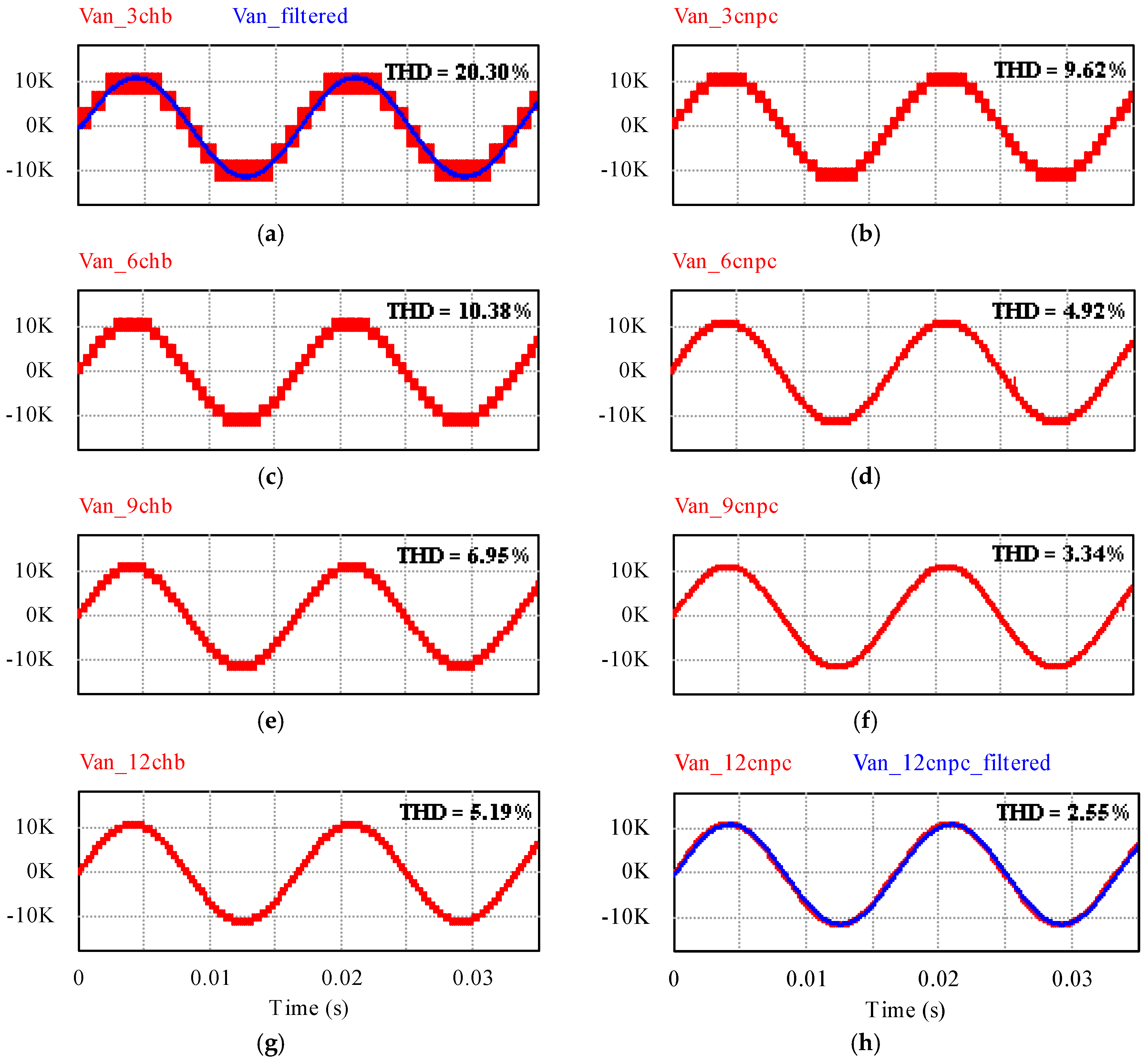
Each port of the cascaded NPC (CNPC) inverter (Figure 2) is switched to provide a leg-to-leg 5-level ac output (i.e., ). N number of CNPC inverters produce outputs that are phase-shifted from each other by an angle to yield a (4N + 1) level ac output as discussed later in Section 3. In CHB modulation, the number of levels for N cascaded H-bridges is (2N + 1). So, CNPC provides lower THD than CHB because of having more levels in the cascaded output voltage waveform. Figure 5 shows how the THD is improved with the increase in number of ports (N) and how the CNPC provides better THD than CHB for any number of cascaded ports. In comparison to cascaded H-bridge (CHB) inverter stage, the CNPC bridge uses double the number of switches with lower voltage rating. It is also advantageous in terms of low dv/dt and less harmonic distortion inherent to the multilevel topology.
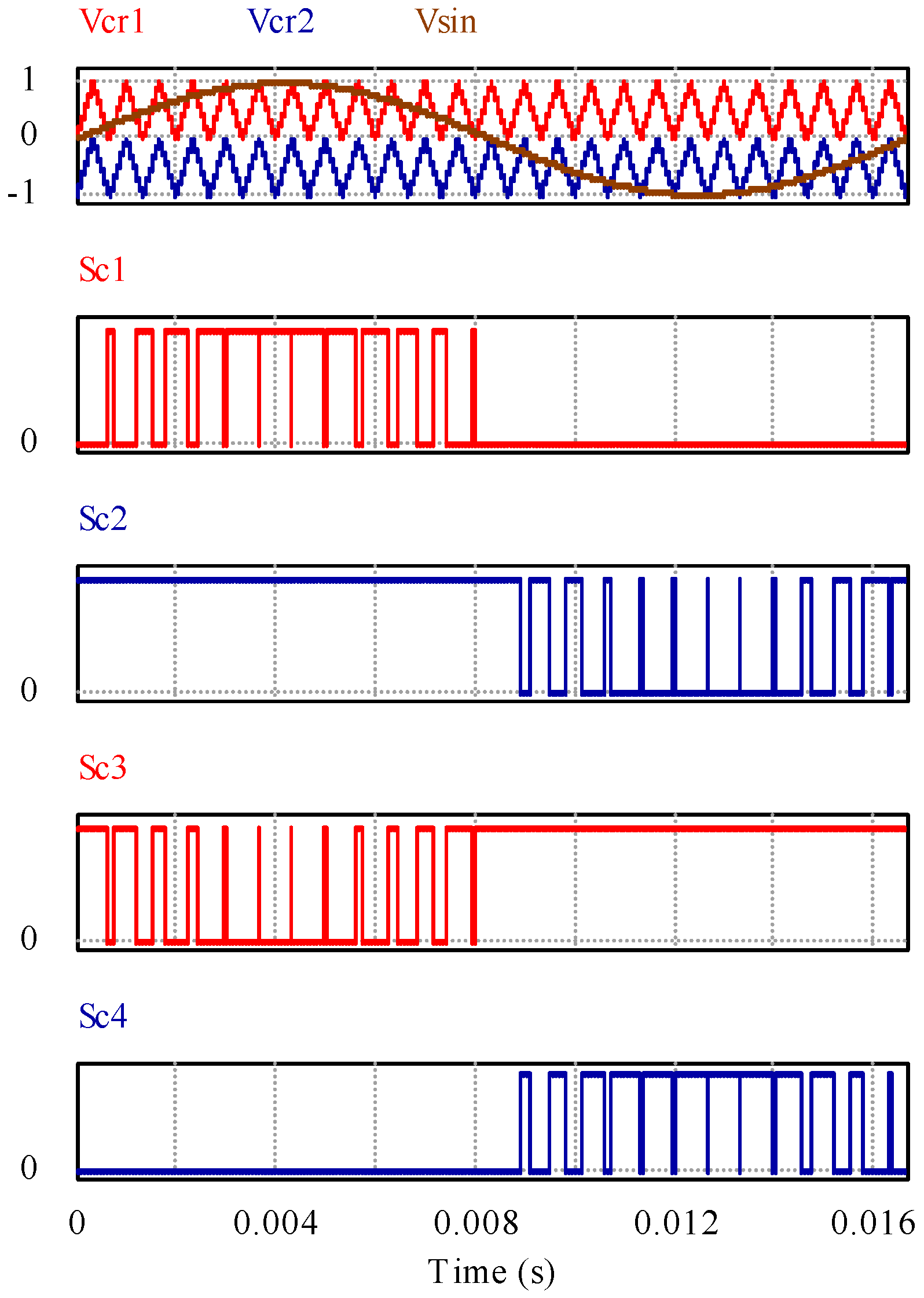
Figure 6 shows how the gate signals are generated for one leg (i.e., leg-c in Figure 2). The signal generation is done by comparing two level-shifted triangular carriers with a sinusoidal modulating waveform. The other NPC leg (i.e., leg-d) has also similar pattern of gate pulses where the modulating signal is shifted by 180°. The carrier frequency has been chosen as 1.5 kHz for easy visualization, though the simulation and hardware experiments have been performed using higher switching frequency. The simulation and hardware output waveforms are shown under Section 3 and Section 4.
2.3. Calculation of Power Stage Paramaters
In order to validate the control and power flow in the proposed converter configuration, a 500 kW3-ph converter has been chosen for design purpose. In that case, the per-phase power output should be:
Assuming the converter having N ports in each phase, each port should process:
The 500 kW 3-phase (i.e., 166.67 kW 1-phase) converter is considered to be connected to the 3-phase utility grid at the 13.8 kV voltage level. The voltage level of the converter at every point has been calculated based on 13.8 kV grid voltage and the per-phase line-to-neutral peak voltage at grid interface for one phase (i.e., phase-a) is:
Assuming a 4% reserve the nominal dc voltage at the input of N inverter ports should be:
For a N-port design of the overall single-phase converter (Figure 2), the input voltage at each inverter port is:
This dc voltage is the output from the 1-port ML-DAB. For example, if N = 9 the dc-link voltage Due to the NPC configuration, the switches on the output side bridge of ML-DAB will withstand half of this voltage, i.e., as shown in Figure 2.
The primary bridge dc voltage of the ML-DAB is actually the output voltage from the PV array. Large scale PV installations usually generate PV power at a voltage level up to 600 V or 1000 V dc. This maximum PV voltage is usually constrained by the PV panel characteristics. Considering the SunPower®, E20-435 (SunPower Corporation, San Jose, CA, USA) (435 W, 72.9 V, 5.97 A) solar panel, 45 panels are required at each port for N = 9. So, 9 series connected panels should make one string with output. Five such strings should be connected in parallel to make a 19 kW array of 45 PV panels. In this case PV array voltage is:
2.4. Selection of Semiconductor Switches
2.4.1. Choosing Semiconductor Switches for the NPC Inverter
In comparison to CHB inverter stage, the CNPC bridge uses double the number of switches with half the voltage rating (e.g., 1700 V rated IGBTs instead of 3300 V). It is also advantageous in terms of low dv/dt inherent to the multilevel topology. In the kV voltage levels, typically lower the voltage rating cheaper the semiconductor switches cost. For example, an Infineon 1.7 kV, 340 A dual IGBT module (Part #FF225R17ME3) costs $124.58 each and from the same manufacturer Infineon, a 3.3 kV, 330 A dual IGBT module (Part #FF200R33KF2C) costs $648.56 [31]. At higher voltage and higher current level this price difference gets more and it becomes a key factor while choosing semiconductor switches for a cost-effective converter design.
In early 1900 it has been discovered that cosmic rays cause random failure of high voltage semiconductor devices which depends on the blocking voltage of the device, junction temperature and altitude. In order to select the proper switching devices (e.g., IGBT, Diode) in the kV range the cosmic ray effect on device failure must be considered for reliable operation. For IGBT modules with voltage rating higher than 1700 V, a DC Stability voltage (VCED for Infineon®) or device commutation voltage (Vcom@100FIT) is mentioned in the manufacturer datasheet. 100 FIT means 100 failures within 109 h of time. This failure is influenced by the device blocking voltage, junction temperature and altitude although the effect of junction temperature and altitude is negligible at room temperature and sea level [32]. As per Equation (16) the dc stability voltage at 100 FIT has been calculated for 1.7 kV, 2.5 kV, 3.3 kV, 4.5 kV and 6.5 kV IGBTs:
Here C1, C2, C3 are parameter values found from [32]. Based on this VCE@100 FIT voltage value, another metric named “device voltage utilization factor (DVUF)” can be defined to choose an IGBT for cost-efficient design [18]. DVUF is defined as:
Here, is the maximum rated voltage mentioned in the IGBT manufacturer datasheet. In order to choose an IGBT module higher DVUF percentage is preferred for an optimum design of the converter. This factor not only optimizes the device utilization efficiency it also reduces the cost of IGBTs in most of the cases. The following Table 1 summarizes the required IGBT voltage rating for both CHB and CNPC inverters for N = 3 to 12.
2.4.2. Choosing Semiconductor Switches for the ML-DAB
For the ML-DAB dc-dc converter the NPC-bridge IGBTs have the same voltage rating as calculated for the NPC inverter in Table 1. The primary bridge of the ML-DAB is a 2-level full-bridge. Usually the PV voltage lies within 1000 V dc limit. If the input voltage is within 720 V (assuming 60% of the VCES of 1.2 kV IGBTs), 1200 V IGBTs can be chosen for primary ML-DAB full-bridge.
For PV voltages in 720 V to 1000 V range, 1700 V IGBTs are a good choice for the same full-bridge. The parameter values obtained for designing a 3-phase 500 kW N-port (i.e., N = 3, 5, 8, 12) PV converter are summarized in Table 2 below. The PV output voltage (Vs) has been chosen based on the string combination of SunPower® E20-435 (SunPower Corporation, San Jose, CA, USA) panels. Based on the power requirement more parallel strings can be combined to form a suitable PV array.
In choosing the no. of ports for this N-port converter design, the required voltage levels have been considered based on commercially available medium voltage IGBTs (e.g., 1.2 kV, 1.7 kV, 2.5 kV, 3.3 kV, 4.5 kV and 6.5 kV). The diodes and capacitors used in the converter is rated as per the IGBT rating associated with those diodes and capacitors. Some high voltage silicon carbide (SiC) based IGBTs have been discussed in literature [33,34,35] which would be helpful in reducing no. of ports and thus improving the power density of the overall converter.
2.5. Cost-Effectiveness of the Proposed N-Port Converter
Based on the proposed design of the N-port converter and a 3.34 kW hardware prototype, an effort has been made to estimate the proposed converter cost and compare it with a commercially available utility-scale overall PV system. In order to prepare a cost comparison with a conventional 1 MW PV system, authors got the support from a private utility scale PV system contractor in the state of Texas. Due to more number of ports per phase the proposed N-port converter alone is likely to be costlier than the central inverter. The conventional transformer cost is not there in the proposed converter since it eliminates the line frequency transformer with smaller high frequency transformers integrated in dc-dc stage. Still the converter alone is not cheaper than the combination of central inverter and transformer. Most of the cost in the proposed converter comes from the HF transformer. The overall gain can be achieved from balance of systems (BOS) cost. Due to internal higher voltages the corresponding current gets much lower in comparison to the central inverters. This lower current saves money by saving a good amount of copper cable, conduit and switchgear. A summary, with some key components in a 1 MW PV system, has been shown in Table 3. It appears that the proposed N-port converter can be $0.13/watt cheaper than a conventional central inverter in the 1 MW scale. The comparison has been made based on central inverter solution. All the item costs have been estimated based on present market price which may vary as per design, place, manufacturer and other market conditions.
It was also observed that the proposed N-port converter has more than 40% lower footprint in comparison to the combination of central inverter and line frequency transformer.
2.6. Global Efficiency of the Proposed N-Port Converter
The efficiency of a system is defined as the ratio of the output power Pout, and input power Pin. Since the proposed N-port converter consists of N number of cascaded ports, the global efficiency for the proposed N-port converter is the ratio between output power and the total input power which is the summation of individual N-port input power. Hence, the global efficiency of the system is the average efficiency of the cascaded ports. The global efficiency of the 12-port converter is 96.42% based on the obtained simulation results:
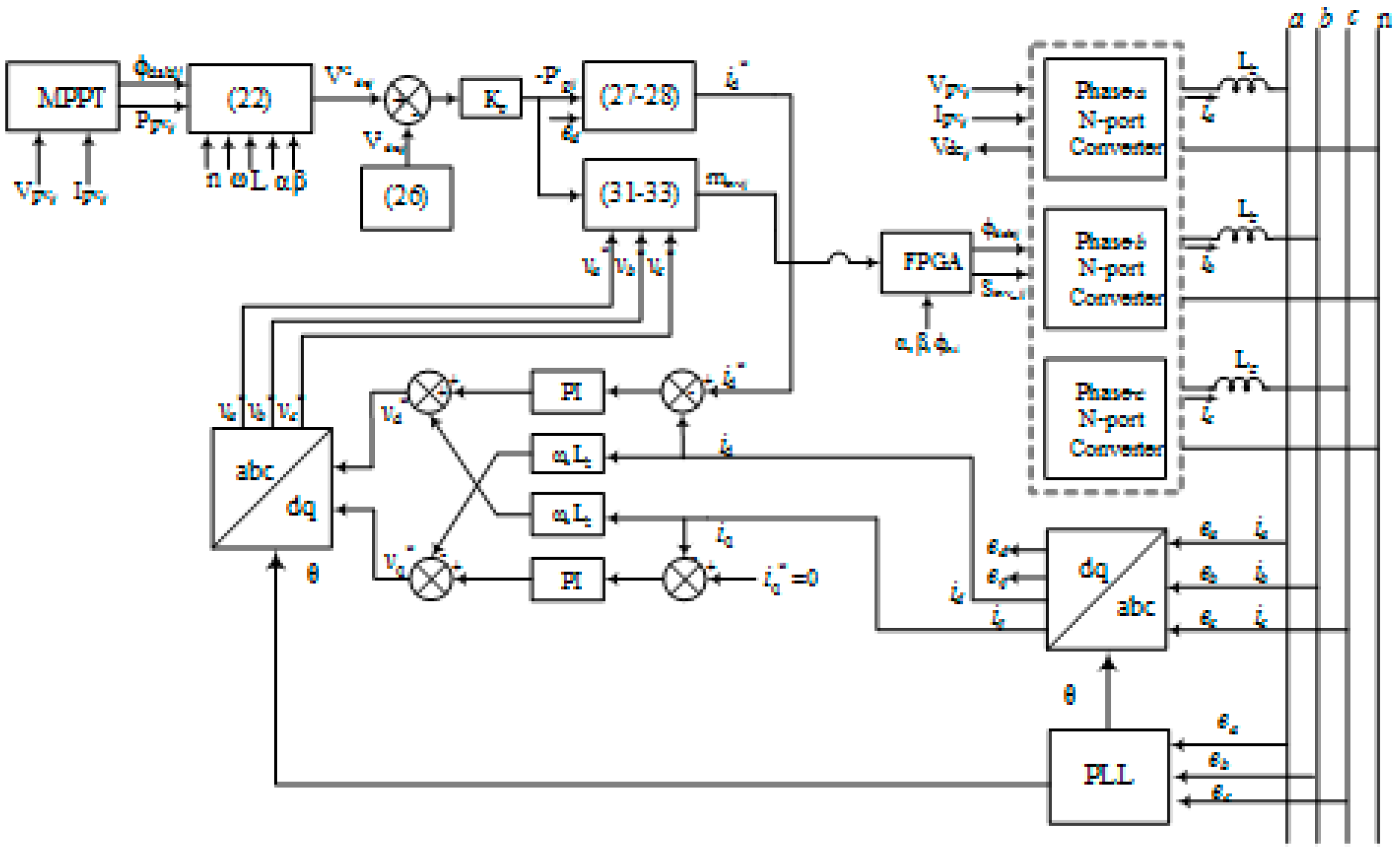
3. Control of N-Port Converter
Since the N-port converter is designed for PV application, the front-end ML-DAB ensures to get the maximum power available from PV array using the MPPT control. MPPT and power mismatch control in the N-port converter will be discussed in the following sub-sections.
3.1. PV Modelling and MPPT Control
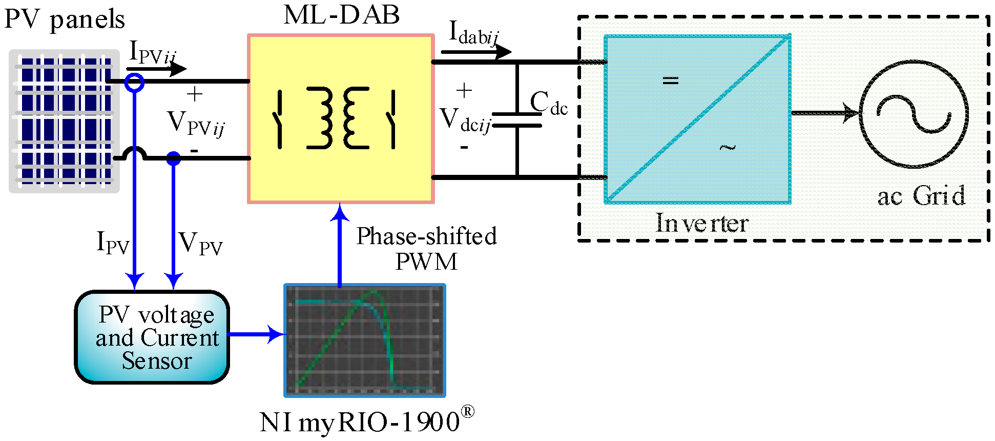
In large scale PV solar system, MPPT is commonly implemented on the inverter stage. In this converter MPPT, using perturb and observe (P&O) method, is achieved by controlling the phase-shift () between the two active bridges in each ML-DAB [36]. The MPPT has also been verified in Simulink® using the incremental conductance algorithm. Based on the variation of insolation, the PV strings generate different currents. To draw the maximum current achievable, thus the maximum power from PV panels, the PV voltage and current are sensed and the derived control signal is translated to desired phase-shift (). Figure 7 shows the block diagram of the grid connected PV system with P&O algorithm implemented in NI myRIO-1900® (National Instruments Corporation, Austin, TX, USA).
Voltage and current sensors are used to sense the slope of PV power curve. A control voltage from the PI controller will accordingly vary the phase shift of (5). A P&O algorithm is implemented to achieve the MPPT control and implemented on LabVIEW® (National Instruments Corporation, Austin, TX, USA) in real time. Phase shifted PWM pulses are generated in LabVIEW FPGA. Once the PV power output is connected to the MPPT circuit the open circuit voltage instantly drops to a new value which is dependent on the impedance of the load. The control algorithm implemented on the NI-myRIO sends corresponding switching pulses to the ML-DAB converter to move the new operating point to the maximum power point (MPP). The detailed MPPT results from hardware are shown in Section 3.
3.2. Capacitor Voltage Mismatch Control at the ML-DAB
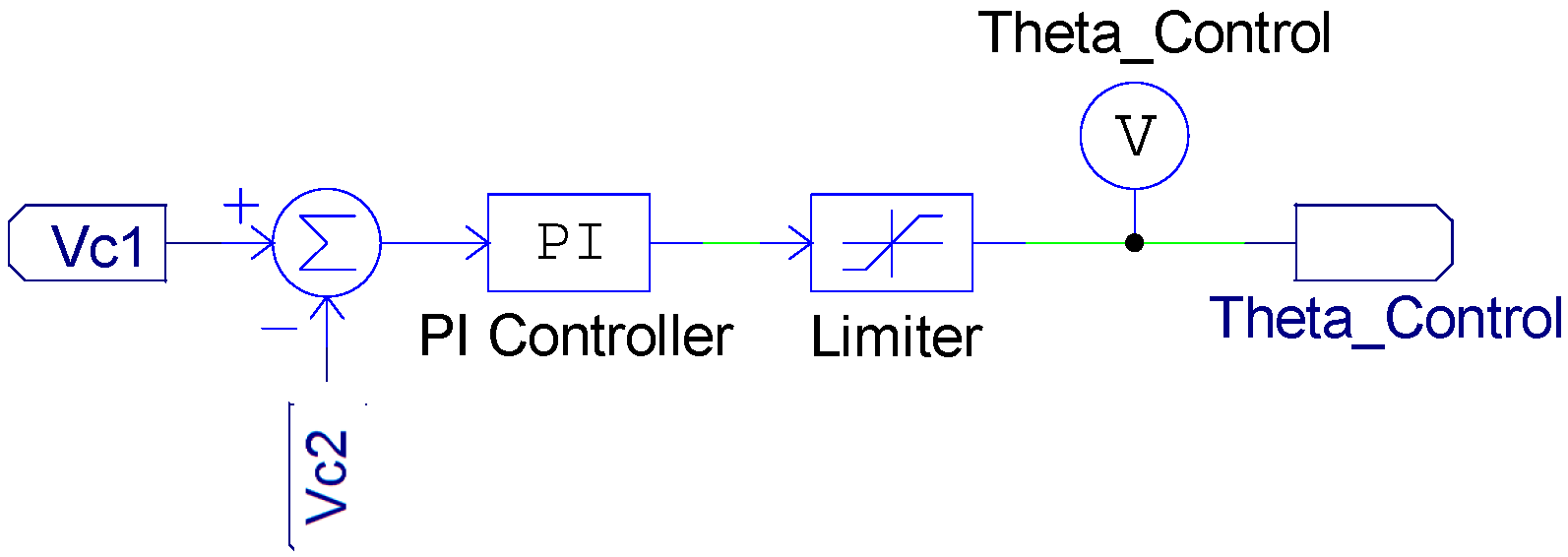
Ideally the ML-DAB should not experience any unbalance between clamping capacitor voltages (Figure 8), where the dc-link voltage , here ports and three phases. Figure 7 shows the dc-link voltage as a series combination of across respectively without showing the common neutral point “o” between ML-DAB NPC bridge and NPC inverter. Due to any load disturbance or converter non-ideality capacitor voltages become unbalanced i.e., During unbalanced condition a non-zero average neutral-point current flows to/away from the neutral point “o” (Figure 7).
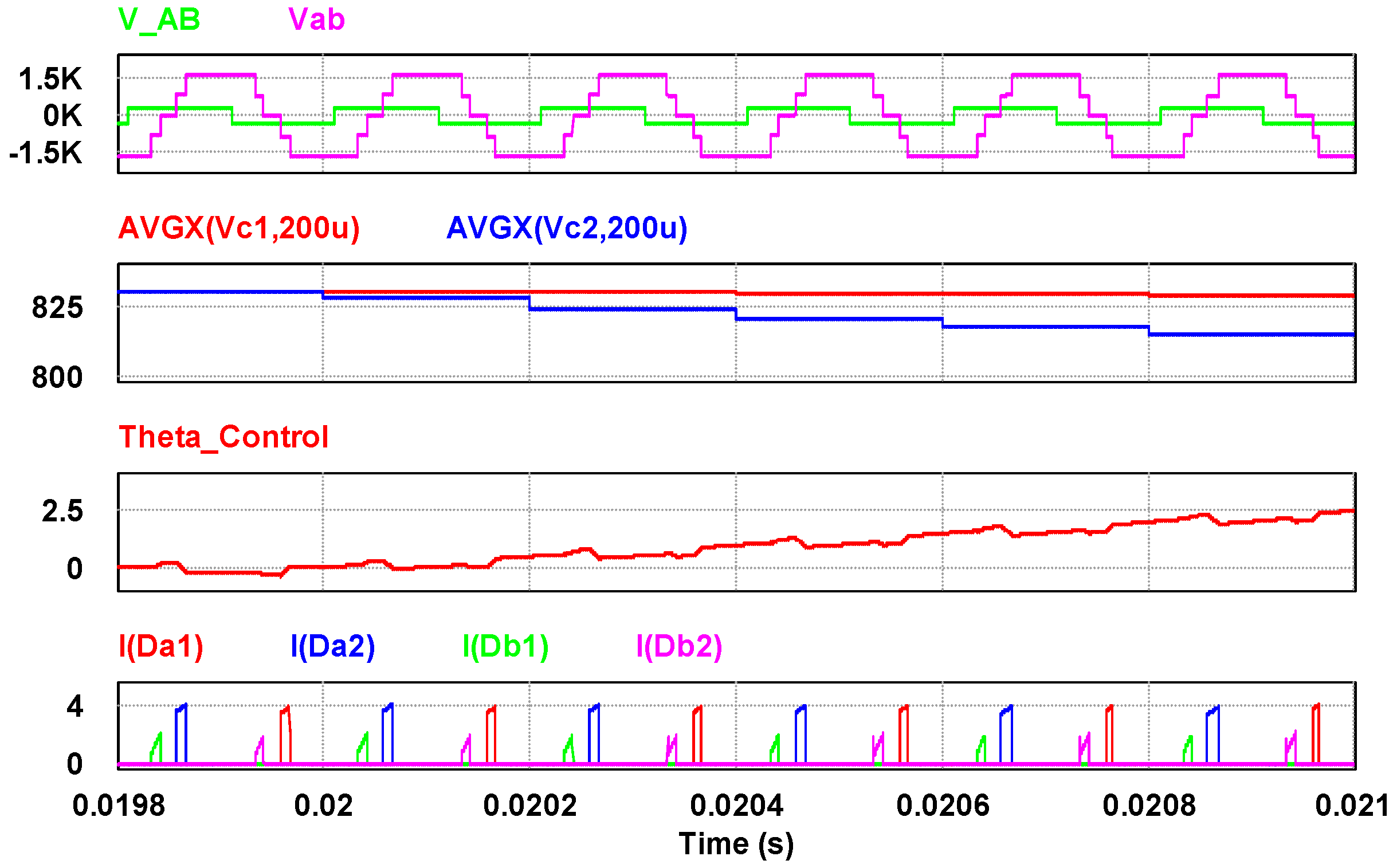
In order to control the switching cycle average of , the diode currents () can be controlled by changing the , which modulates corresponding NPC switch gate pulses accordingly. For example, if during any unbalance then switching-cycle average of () should be reduced and should be increased. In order to implement this control, we need to delay and start earlier by an amount of as shown in Figure 9, Figure 10 and Figure 11 as “Theta_Control” in degrees. During simulation the gain 0.018 and time-constant 0.01413 have been used to validate the control algorithm using a PI controller. A similar capacitor voltage balancing control has been described in [37]. As shown in Figure 11, an intentional imbalance between has been created bypassing a part of the through Rb (Figure 8) at t = 0.02.
3.3. dc-Link Voltage Control Using Power Mismatch among N Ports
Voltage imbalance and power mismatch among the different ports are control challenges for a multiport cascaded converter topology. Various control strategies have been described in literature in order to regulate such unbalance for cascaded inverters in solid state transformer (SST) applications [22,25]. The overall control structure has been designed, in this paper, based on the input PV power mismatch among the various ports in all three phases. Maximum power point current and corresponding voltage can be obtained from the MPPT control. The product of and is the output power from the solar PV panels which is fed into the dc-dc ML-DAB converter. Assuming as the efficiency for ML-DAB dc-dc stage conversion, we get:
For N numbers of ports per phase, the total power to be processed in three phases should be:
The dc-dc ML-DAB power equation for one port is as follows. Here are assumed to be constant and varies according to MPPT control (Figure 3):
ML-DAB output current can be obtained by using the variables such as , , , n, w, L and as follows:
As there will be difference in power from the PV panels connected to different ports, it is necessary to find the ratio of the individual port’s PV power to the total PV power:
The respective ratio of the individual ports is multiplied by d-axis grid current and d-axis grid voltage , obtained from transformation, to calculate the inverter input power for the respective port of the N-port converter (Figure 12 and Figure 13). In order to establish the decoupled control of active power through control of , and reactive power through in the grid voltage-oriented control, where is zero and equals times the amplitude of the grid phase voltage:
An approach to control the dc-link voltage has been described in [24] for a doubly fed induction generator (DFIG). This can be modified in the proposed N-port converter for balancing the power mismatch among different ports. The energy stored in a small time period in the dc-link capacitor can be expressed as the power difference between and at any instant (Figure 13). The reference DC bus voltage can be obtained from Equation (27):
Considering as the control variable and assuming as constant (i.e., perturbation in to be zero), the small signal model can be derived from Equation (27), as shown in Equation (28):
The controller parameters can be found from Equation (28). The square of measured dc-link voltage is compared with the reference obtained from Equation (23) to regulate the dc-link voltage. This yields the active power reference (Figure 12). This power gives the reference for as shown in Equation (29), where is the -axis component of grid voltage and is calculated from Equation (30) to Equation (31):
The ac output voltage from every single inverter port can be obtained by multiplying the reference grid phase voltage (e.g., ) with the respective negative power reference () ratio as shown in Equation (32):
Similarly, the ac output from all other ports can be obtained for phases and c as shown below:
The sum of the output voltages from each of N-port inverters appears across the respective phase of the grid (i.e., ):
The current flowing towards the grid () can be found using equations (36) to (38), where are respective grid voltages and are the lumped resistance and inductance respectively at the grid interface:
Assuming balanced grid currents, the sum grid currents is zero:
Using transformation, grid currents are transformed into and (Figure 12). Current is compared with the corresponding reference current , and is assumed to be zero. The output of the -phase PI controller is summed up with the product of , and current and the resultant is the -phase reference voltage . can be obtained similarly as shown in Figure 12. After the dq − abc transformation reference voltages , , can be obtained. These reference voltages are used as the modulating signal for the level-shifted PWM to generate the corresponding gate pulses () for the IGBTs used in the NPC inverters. The phase-shift control parameter () has been derived independently from the MPPT control which generates the gate pulses for the ML-DAB primary bridge switches () corresponding to the required phase-shift () between two bridges.
3.4. (N − 1) Redundancy
The overall converter has been studied for (N − 1) redundancy. That means, if a single port out of the N numbers of total ports per phase fails, the whole converter should not stop functioning. Because of one port failure, each of the remaining ports has to deal with a higher voltage to still maintain the grid voltage at the output. In order to safeguard the IGBTs from excessive voltage this redundancy design is feasible for higher number of ports (e.g., N = 9 or more). The parameter values have been considered from Table 2 with to study the effect of 1-port failure among the numbers of ports. For And the ML-DAB output voltage and ; and The total power (i.e., ) at the inverter output will be reduced to (() due to 1-port failure. The current through the cascaded NPC bridges at the inverter output stage will be reduced to comply with this reduction in total power. Assuming power from every single ML-DAB port remains the same and it is obtained from PV MPPT control. (for 1-port) should also remain same as before since is controlled by the MPPT controller to achieve maximum available power from the PV panels. Only will go high to maintain constant grid voltage. The turns ratio n and leakage inductance of the high frequency transformer will also remain the same as this is a parameter value obtained from hardware design. The switching frequency is also kept constant. The phase-shift between the outputs of the CNPC inverters change from to in the case of 1 port failure. Assuming 12 number of ports per phase (i.e., N = 12), Table 4 summarizes the calculated parameter values for a single port converter in case of 1 port failure (i.e., N −1 = 11).
4. Simulation and Experimental Results
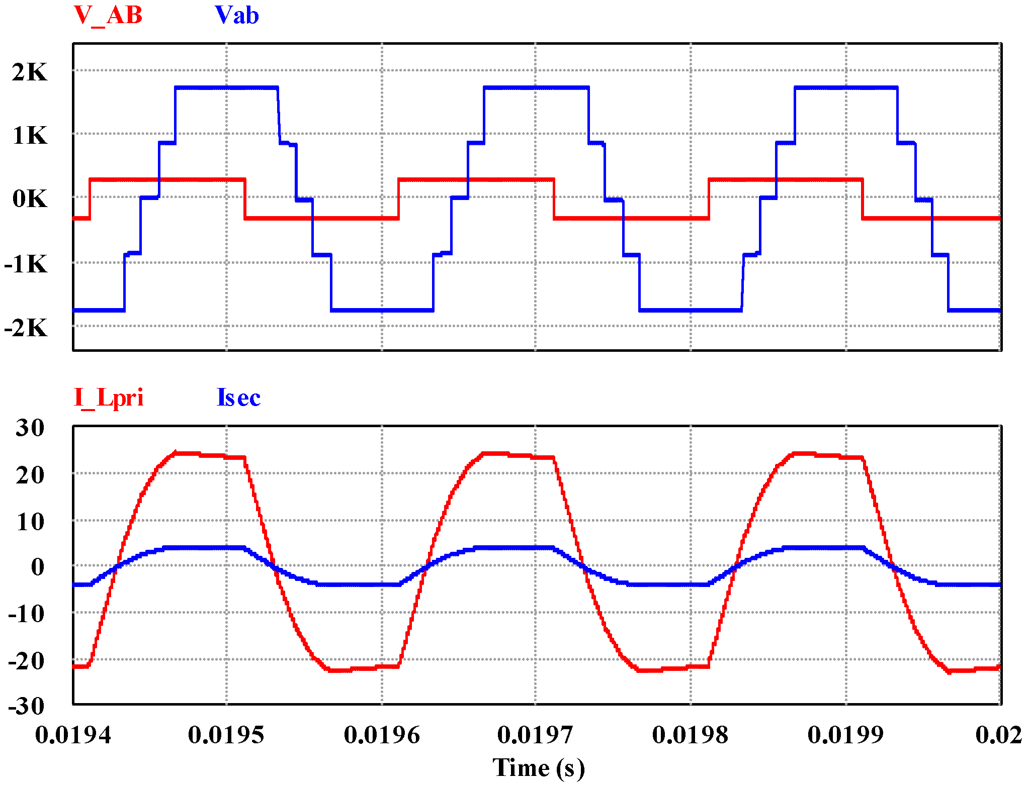
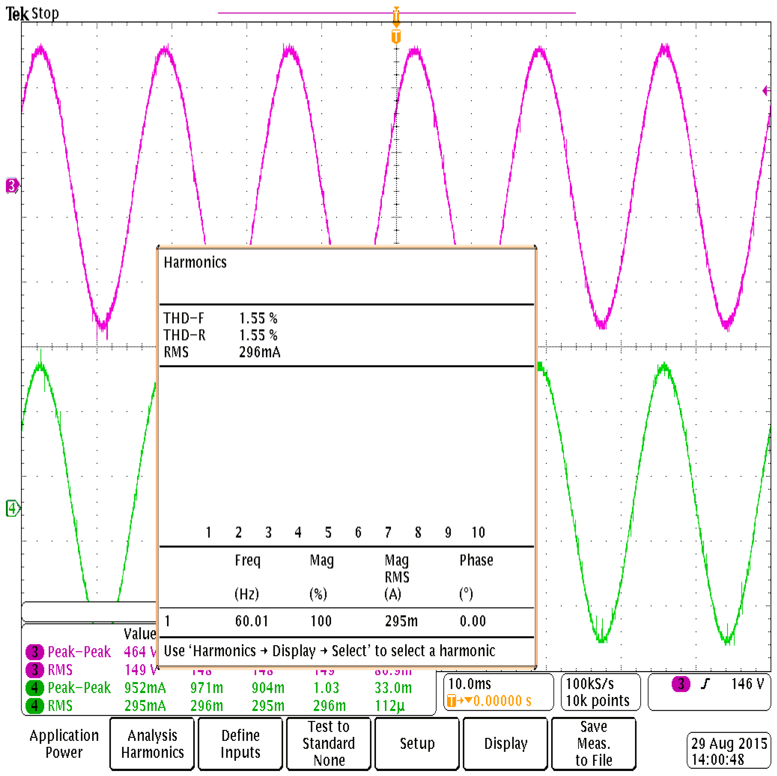
Each port (i.e., ML-DAB and NPC inverter) has been designed to process 3.34 kW of power for simulation and hardware experiments. Table 1 shows the voltage levels and parameter values for one port, which has been derived assuming the output of the cascaded NPC (CNPC) bridge is connected to the 13.8 kV utility grid. In order to realize the switching and conduction losses Infineon FF100R12YT3 dual IGBT module and IXYS DSEP 30-12AR clamping diodes are modeled in PSIM® thermal module simulation software. The same IGBTs and diodes are used in the hardware prototype also. The voltage conversion ratio in the ML-DAB is chosen as unity resulting in the turns ratio The switching frequency is set at 5 kHz. Figure 14 shows the simulated steady state voltage and current waveforms across the high frequency transformer in the ML-DAB where α = 10°, β = 30°.
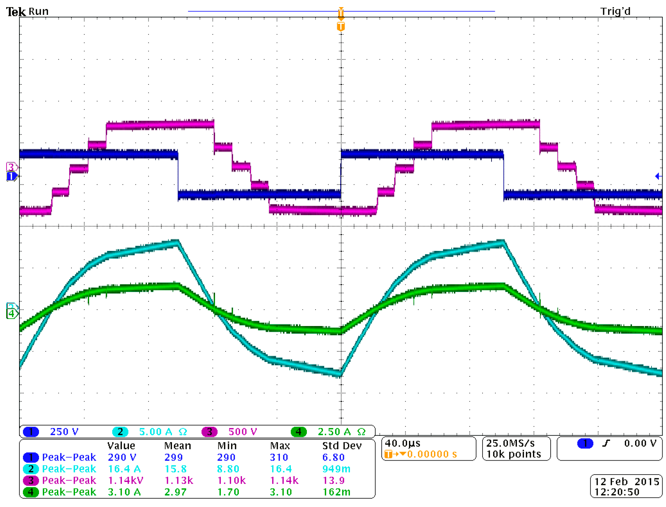
A scaled down laboratory prototype of the proposed converter (ML-DAB and NPC inverter) has been built for validating the MPPT and power flow control and to observe the key waveforms at different stages of power conversion assuming open loop operation. Each ML-DAB and NPC inverter hardware has been designed to process a maximum 3.34 kW of power. The value of varies according the control signal received from the MPPT sub-circuit. Figure 15 shows the experimental waveforms of the ML-DAB for α = 10°, β = 30°, φ = 70°.
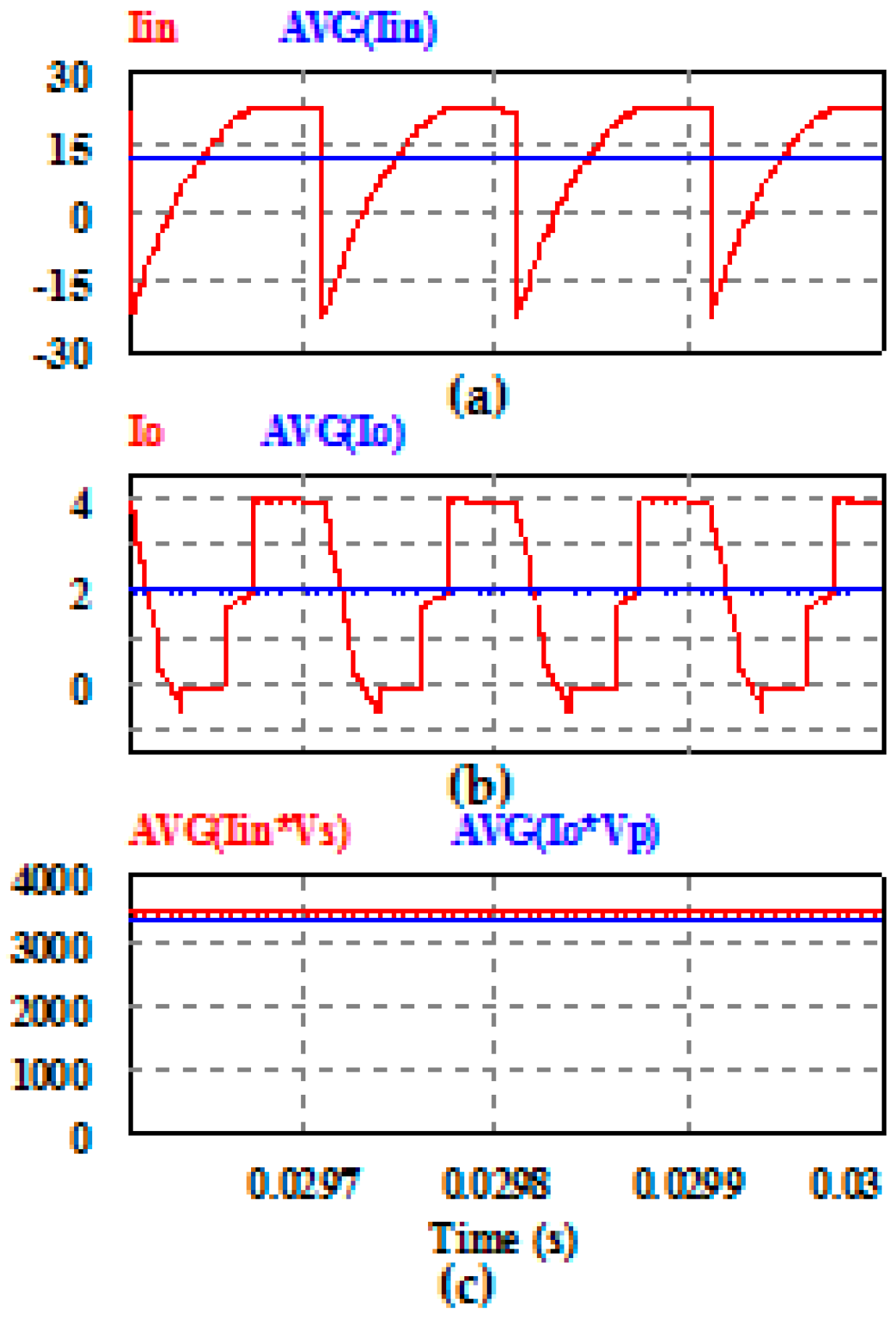
Figure 16 and Figure 17 show the simulated and experimental input-output currents at ML-DAB. MPPT control in ML-DAB adjusts the phase shift to obtain the maximum power available at the PV panels. The ML-DAB input voltage () is obtained from four PV panels in series. The PV parameters have been calculated based on the SunPower® E20-435W, 72.9 V, 5.97 A solar panel datasheet. Figure 18 shows the effect of MPPT control and phase-shift modulation when PV current changes due to the change in solar irradiance for both Perturb and Observe (P&O) and Incremental Conductance algorithm.
NI-myRIO® (National Instruments Corporation, Austin, TX, USA) has been used to provide MPPT control signals for ML-DAB converter. The MPPT algorithm and the phase-shift PWM scheme is built, debugged and run with the help of LabVIEW development software. A voltage transducer (SCK-MU-1500V) has been used at the point where the PV module output is connected to the input of the DAB converter to measure the dc input voltage. A current transducer (CR5410-20) measures the PV generated current of the PV module on each operating point. The MPPT algorithm provides the required phase-shift () which gives the gate-pulse for the ML-DAB primary bridge switches. This phase shift allows the required amount of power, generated from PV MPPT, to flow through the ML-DAB to the inverter and the load. Figure 19 shows the MPPT results obtained from hardware using MAGNA Power® XR200-10 (MAGNA Power Electronics Inc., Flemington, NJ USA) PV source emulator and NI myRIO-1900® FPGA (National Instruments Corporation, Austin, TX, USA) (Figure 20).
MPPT efficiency is determined, as the ratio of power measured with the MPPT controller and the true power, the PV module produces without the MPPT controller:
The true power of PV array at irradiance 1000 W/m2 and 800 W/m2 from PV source emulator is given as 96.3 W and 75.35 W respectively. Thus the MPPT efficiency is 97.6% for 1000 W/m2 and 98.2% for 800 W/m2.
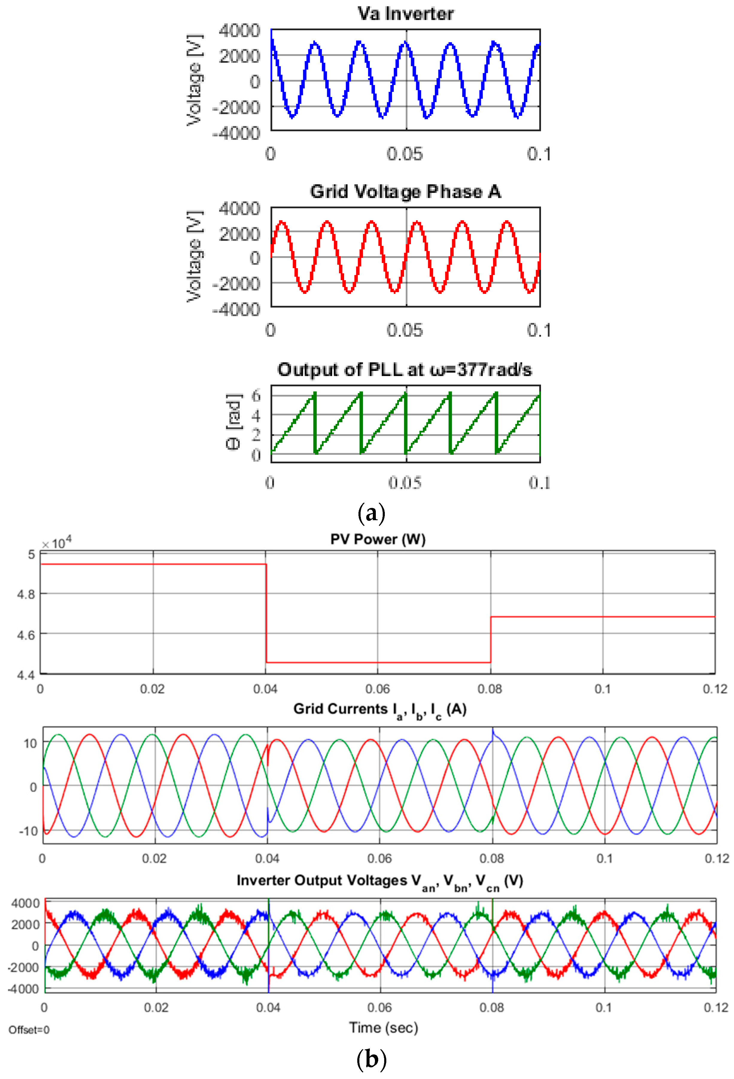
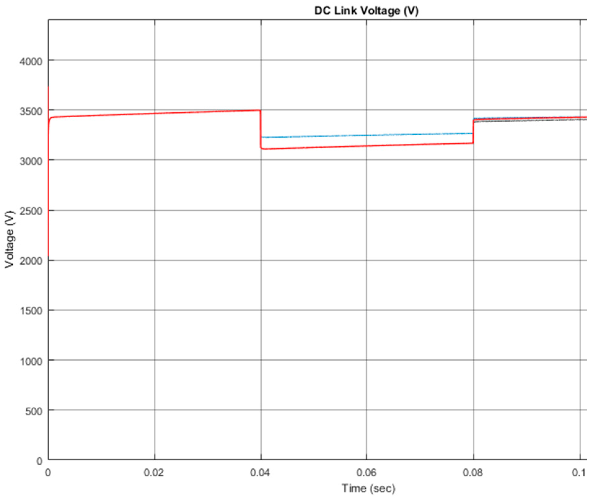
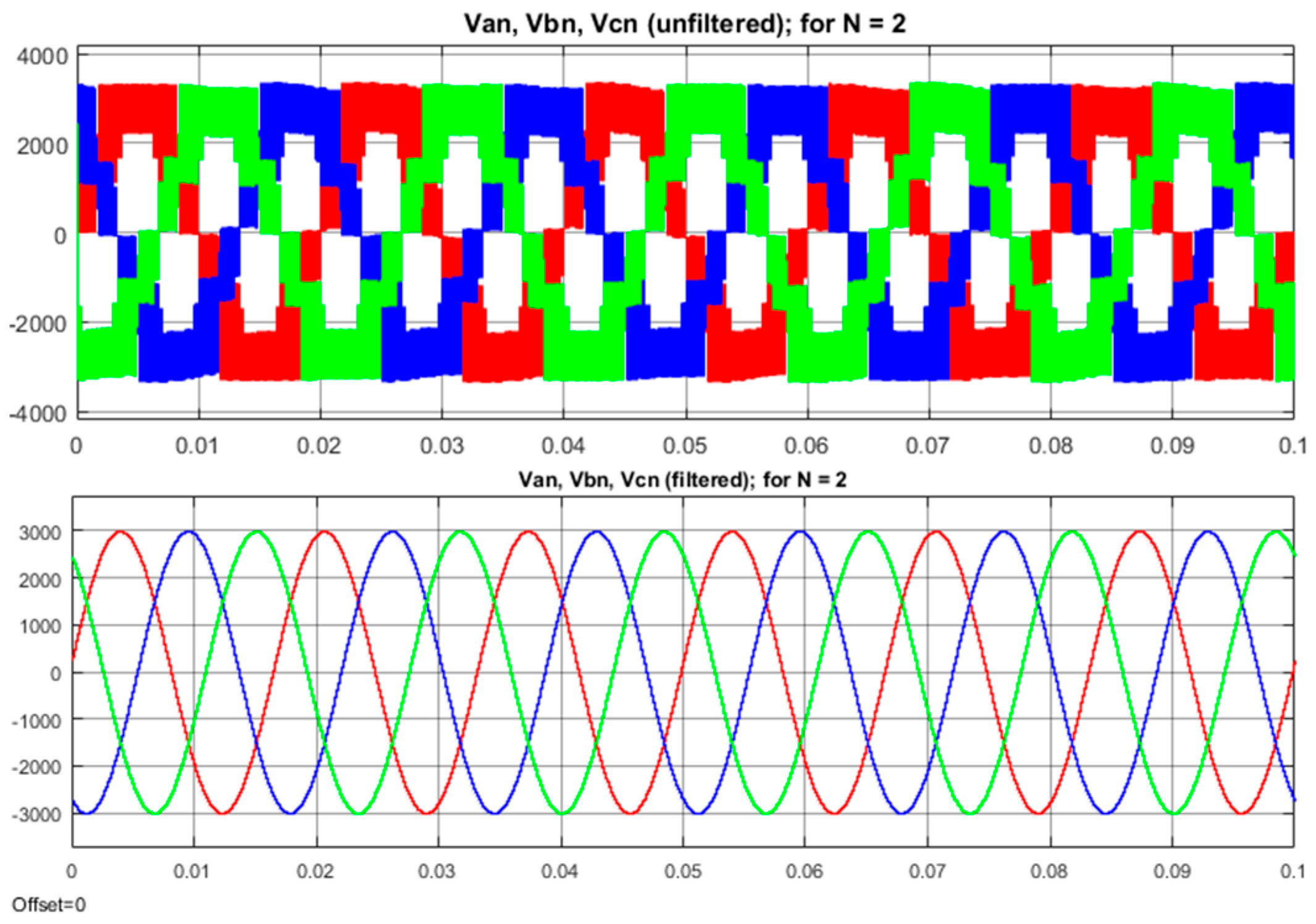
The current control for grid-connected N-port converter has been performed in Simulink® (The MathWorks Inc., Natick, MA, USA). For clarity in the waveforms to present in this paper, five ports () per phase have been considered. The control scheme uses PLL to provide a phase reference and establish the frequency at the inverter terminals. Figure 21a shows the PLL response of a three phase system synchronized with the grid at the frequency of 60 Hz. The PV power input to different ports has been changed at two time instants (i.e., at t = 0.04 s and at t = 0.08 s) to observe the control performance as shown in Figure 21b. Figure 22 and Figure 23 show the dc-link voltage control using two CHB inverters per phase. Details of this control algorithm has been described in Section 3.3.
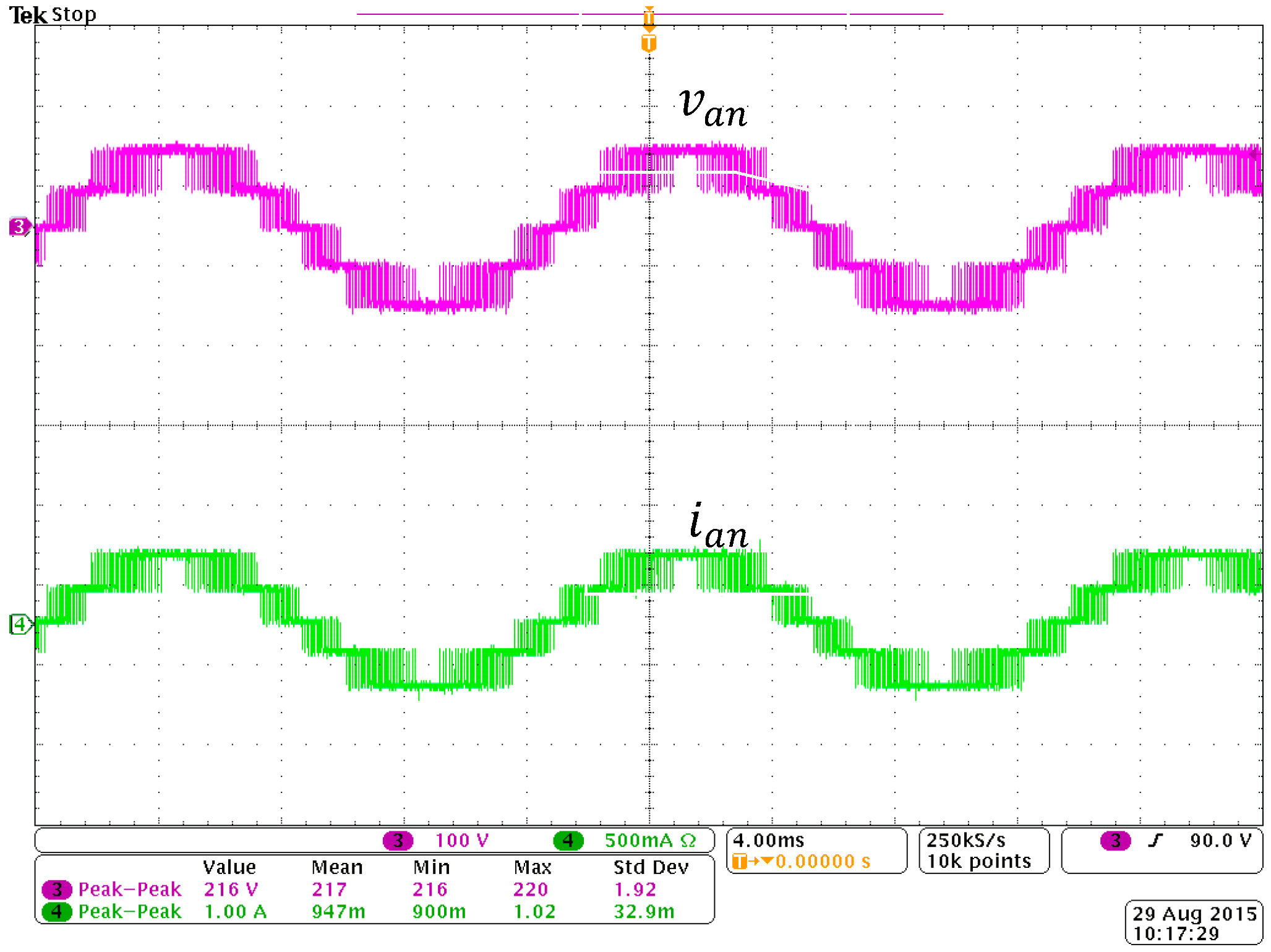
Figure 24 and Figure 25 show how the NPC inverter ports improve the output ac waveform in terms of THD. The experimental results, obtained from two 3.34 kW prototypes cascaded, are shown in Figure 26 and Figure 27.
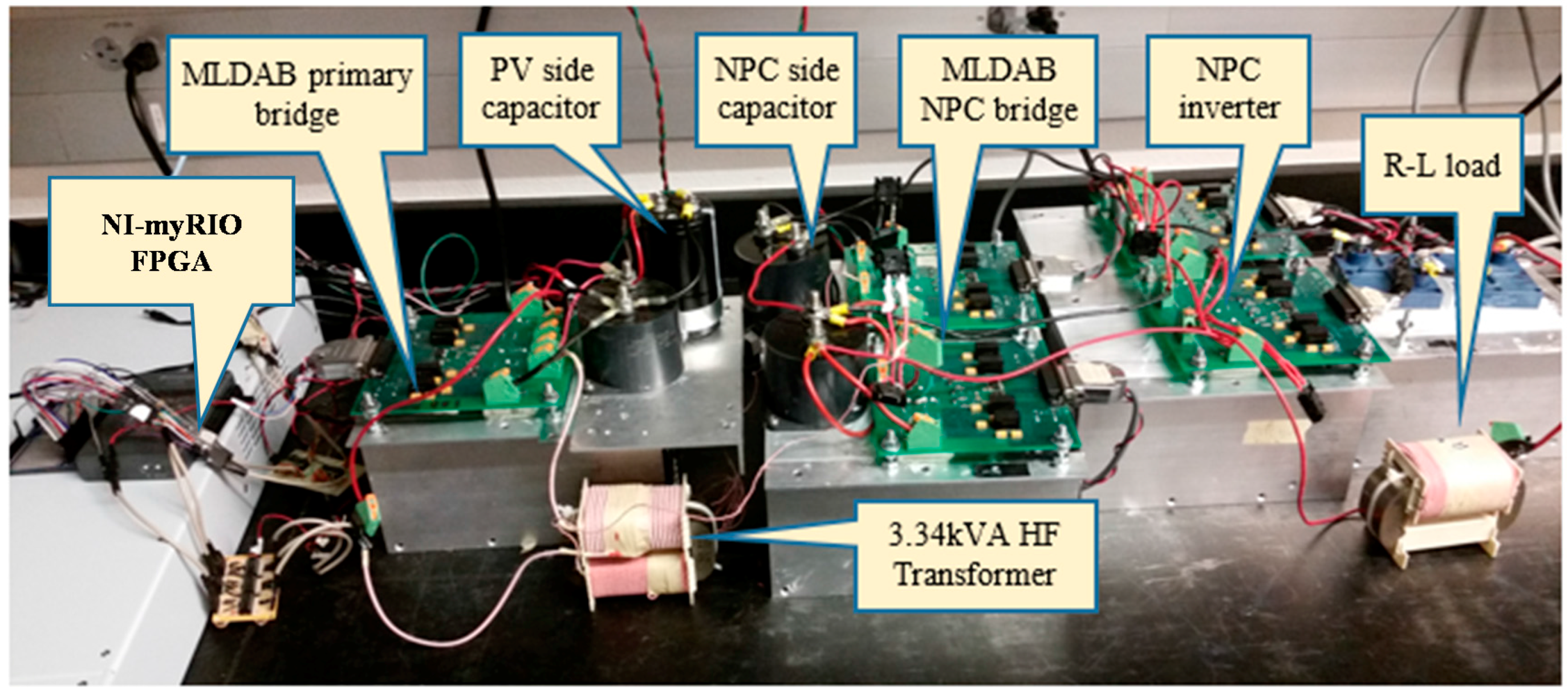
The hardware set-up for one port of 3.34 kW prototype converter (ML-DAB and NPC inverter) is shown in Figure 28 with a resistive-inductive load. The experiments have been performed at a scaled-down power level with a maximum ML-DAB input dc voltage () of 125 V. The hardware components used in one port of the proposed converter are summarized in Table 5 below.
5. Conclusions
A distributed modular N-port converter configuration, using neutral point diode clamped multilevel DAB and cascaded NPC-bridge inverters with high frequency transformer integration, has been presented for utility scale grid-connected PV system. A novel dc-dc multi-level DAB with MPPT scheme is presented as an intermediate dc-dc converter stage. Detailed design of the power stage parameters is shown and the control strategy based on power mismatch among the various ports has been proposed and verified in simulation in PSIM® and Simulink®. Experimental outputs are obtained from two ports of hardware prototype running under laboratory test condition. The steady-state analysis of the converter has been performed both in simulation and using hardware prototypes to validate the power flow and overall performance of the converter.
Acknowledgments
This work is supported by the United States Department of Energy under Award No. DE-EE0006323.
Author Contributions
Hariharan Krishnaswami conceived the concept; M.A. Moonem, Turgay Duman performed analysis; Turgay Duman designed and performed the experiments; Shilpa Marti and Hariharan Khrisnaswami analyzed the data; Azas Ahmed Rifath Abdul Kader verified mismatch control algorithm; Hariharan Khrisnaswami mentored students M.A. Moonem, Turgay Duman, Shilpa Marti, and Azas Ahmed Rifath Abdul Kader; M.A. Moonem, and Turgay Duman wrote the paper. All authors approved the final manuscript.
Conflicts of Interest
The authors declare no conflict of interest.
References
- ALENCON. Available online: http://alenconsystems.com/wp-content/uploads/2014/10/GrIP_Datasheet-2.pdf (accessed on 16 May 2015).
- Schmalzel, J.; Jansson, P.; Schmalzel, D.; Schwabe, U.; Fishman, O. Novel inverter technology reduces utility-scale pv system costs. In Proceedings of the 2011 37th IEEE Photovoltaic Specialists Conference (PVSC), Seattle, WA, USA, 19–24 June 2011; pp. 1869–1871. [Google Scholar] [CrossRef]
- Idaho_National_Lab. Transformer Efficiency Assessment—Okinawa, Japan. Available online: https://inldigitallibrary.inl.gov/sti/5516342.pdf (accessed on 20 June 2014).
- Kouro, S.; Leon, J.I.; Vinnikov, D.; Franquelo, L.G. Grid-connected photovoltaic systems: An overview of recent research and emerging pv converter technology. IEEE Ind. Electron. Mag. 2015, 9, 47–61. [Google Scholar] [CrossRef]
- Calais, M.; Agelidis, V.G. Multilevel Converters for Single-Phase Grid Connected Photovoltaic Systems—An Overview. In Proceedings of the 1998 IEEE International Symposium on Industrial Electronics (ISIE’98), Pertoria, South Africa, 7–10 July 1998; Volume 221, pp. 224–229. [Google Scholar] [CrossRef]
- Freddy, T.K.S.; Rahim, N.A.; Hew, W.P.; Che, H.S. Comparison and analysis of single-phase transformerless grid-connected pv inverters. IEEE Trans. Power Electron. 2014, 29, 5358–5369. [Google Scholar] [CrossRef]
- Islam, M.R.; Guo, Y.; Zhu, J. A multilevel medium-voltage inverter for step-up-transformer-less grid connection of photovoltaic power plants. IEEE J. Photovolt. 2014, 4, 881–889. [Google Scholar] [CrossRef]
- Essakiappan, S.; Krishnamoorthy, H.S.; Enjeti, P.; Balog, R.S.; Ahmed, S. Multilevel medium-frequency link inverter for utility scale photovoltaic integration. IEEE Trans. Power Electron. 2015, 30, 3674–3684. [Google Scholar] [CrossRef]
- Kjaer, S.B.; Pedersen, J.K.; Blaabjerg, F. A review of single-phase grid-connected inverters for photovoltaic modules. IEEE Trans. Ind. Appl. 2005, 41, 1292–1306. [Google Scholar] [CrossRef]
- Meneses, D.; Blaabjerg, F.; Óscar, G.; Cobos, J.A. Review and comparison of step-up transformerless topologies for photovoltaic ac-module application. IEEE Trans. Power Electron. 2013, 28, 2649–2663. [Google Scholar] [CrossRef]
- Koutroulis, E.; Blaabjerg, F. Design optimization of transformerless grid-connected pv inverters including reliability. IEEE Trans. Power Electron. 2013, 28, 325–335. [Google Scholar] [CrossRef]
- Huang, A.Q. FREEDM SYSTEM—A vision for the future grid. In Proceedings of the IEEE PES General Meeting, Providence, RI, USA, 25–29 July 2010; pp. 1–4. [Google Scholar] [CrossRef]
- Zhang, L.; Sun, K.; Feng, L.; Wu, H.; Xing, Y. A family of neutral point clamped full-bridge topologies for transformerless photovoltaic grid-tied inverters. IEEE Trans. Power Electron. 2013, 28, 730–739. [Google Scholar] [CrossRef]
- Lesnicar, A.; Marquardt, R. An innovative modular multilevel converter topology suitable for a wide power range. In Proceedings of the 2003 IEEE Bologna Power Tech Conference, Bologna, Italy, 23–26 June 2003; Volume 3, p. 6. [Google Scholar] [CrossRef]
- Nichols, S.; Huang, J.; Ilic, M.; Casey, L.; Prestero, M. Two-stage pv power system with improved throughput and utility control capability. In Proceedings of the 2010 IEEE Conference on Innovative Technologies for an Efficient and Reliable Electricity Supply (CITRES), Waltham, MA, USA, 27–29 September 2010; pp. 110–115. [Google Scholar] [CrossRef]
- Rivera, S.; Kouro, S.; Wu, B.; Leon, J.I.; Rodriguez, J.; Franquelo, L.G. Cascaded h-bridge multilevel converter multistring topology for large scale photovoltaic systems. In Proceedings of the 2011 IEEE International Symposium on Industrial Electronics, Gdansk, Poland, 27–30 June 2011; pp. 1837–1844. [Google Scholar] [CrossRef]
- Liming, L.; Hui, L.; Yaosuo, X.; Wenxin, L. Decoupled active and reactive power control for large-scale grid-connected photovoltaic systems using cascaded modular multilevel converters. IEEE Trans. Power Electron. 2015, 30, 176–187. [Google Scholar] [CrossRef]
- Islam, M.R.; Guo, Y.; Zhu, J. A high-frequency link multilevel cascaded medium-voltage converter for direct grid integration of renewable energy systems. IEEE Trans. Power Electron. 2014, 29, 4167–4182. [Google Scholar] [CrossRef]
- Tripathi, A.; Mainali, K.; Patel, D.; Kadavelugu, A.; Hazra, S.; Bhattacharya, S.; Hatua, K. Design considerations of a 15 kV SiC IGBT enabled high-frequency isolated dc-dc converter. In Proceedings of the 2014 International Power Electronics Conference (IPEC-Hiroshima 2014—ECCE-ASIA), Hiroshima, Japan, 18–21 May 2014; pp. 758–765. [Google Scholar] [CrossRef]
- Mainali, K.; Tripathi, A.; Madhusoodhanan, S.; Kadavelugu, A.; Patel, D.; Hazra, S.; Hatua, K.; Bhattacharya, S. A transformerless intelligent power substation: A three-phase sst enabled by a 15-kV SiC IGBT. IEEE Power Electron. Mag. 2015, 2, 31–43. [Google Scholar] [CrossRef]
- Yuxiang, S.; Rui, L.; Yaosuo, X.; Hui, L. High-frequency-link-based grid-tied pv system with small dc-link capacitor and low-frequency ripple-free maximum power point tracking. IEEE Trans. Power Electron. 2016, 31, 328–339. [Google Scholar] [CrossRef]
- Zhao, T.; Wang, G.; Bhattacharya, S.; Huang, A.Q. Voltage and power balance control for a cascaded h-bridge converter-based solid-state transformer. IEEE Trans. Power Electron. 2013, 28, 1523–1532. [Google Scholar] [CrossRef]
- Kouro, S.; Wu, B.; Moya, A.; Villanueva, E.; Correa, P.; Rodriguez, J. Control of a cascaded h-bridge multilevel converter for grid connection of photovoltaic systems. In Proceedings of the 2009 35th Annual Conference of IEEE Industrial Electronics (IECON’09), Porto, Portugal, 3–5 November 2009; pp. 3976–3982. [Google Scholar] [CrossRef]
- Vijay Vittal, R.A. Grid Integration and Dynamic Impact of Wind Energy; Springer: New York, NY, USA, 2013; ISBN 978-1-4419-9323-6. [Google Scholar]
- Wang, L.; Zhang, D.; Wang, Y.; Wu, B.; Athab, H. Power and voltage balance control of a novel three-phase solid state transformer using multilevel cascaded h-bridge inverters for microgrid applications. IEEE Trans. Power Electron. 2015, 31, 3289–3301. [Google Scholar] [CrossRef]
- Yu, Y.; Konstantinou, G.; Hredzak, B.; Agelidis, V.G. Power balance of cascaded h-bridge multilevel converters for large-scale photovoltaic integration. IEEE Trans. Power Electron. 2016, 31, 292–303. [Google Scholar] [CrossRef]
- Kheraluwala, M.H.; Gascoigne, R.W.; Divan, D.M.; Baumann, E.D. Performance characterization of a high-power dual active bridge. IEEE Trans. Ind. Appl. 1992, 28, 1294–1301. [Google Scholar] [CrossRef]
- Kulasekaran, S.; Ayyanar, R. Analysis, design, and experimental results of the semidual-active-bridge converter. IEEE Trans. Power Electron. 2014, 29, 5136–5147. [Google Scholar] [CrossRef]
- Moonem, M.; Pechacek, C.; Hernandez, R.; Krishnaswami, H. Analysis of a multilevel dual active bridge (ML-DAB) DC-DC converter using symmetric modulation. Electronics 2015, 4, 239. [Google Scholar] [CrossRef]
- ROHM Semiconductor. Available online: http://www.rohm.com/documents/11308/98b20d7a-0c11-4689-b4db-85150574b12c (accessed on 17 March 2015).
- Mouser Electronic Inc. Available online: http://www.mouser.com/Semiconductors/Discrete-Semiconductors/Transistors/IGBT-Modules/_/N-ax1sd/ (accessed on 24 November 2015).
- ABB Ltd. Application Note 5sya 2042-04: Failure Rates of Hipak Modules Due to Cosmic Rays; ABB Ltd.: Zurich, Switzerland, 2011. [Google Scholar]
- Jun, W.; Huang, A.; Woongje, S.; Yu, L.; Baliga, B.J. Smart grid technologies. IEEE Ind. Electron. Mag. 2009, 3, 16–23. [Google Scholar] [CrossRef]
- Wang, X.; Cooper, J.A. High-Voltage n-channel igbts on free-standing 4H-SiC epilayers. IEEE Trans. Electron. Devices 2010, 57, 511–515. [Google Scholar] [CrossRef]
- Xi, X.; Liu, S.; Kuang, J. Research of efficient dc-dc converter based on SiC power devices and zvs soft switches. In Proceedings of the 2013 1st International Future Energy Electronics Conference (IFEEC), Tainan, Taiwan, 3–6 November 2013; pp. 194–198. [Google Scholar] [CrossRef]
- Moonem, M.A.; Krishnaswami, H. Control and configuration of three-level dual-active bridge dc-dc converter as a front-end interface for photovoltaic system. In Proceedings of the 2014 Twenty-Ninth Annual IEEE, Applied Power Electronics Conference and Exposition (APEC), Fort Worth, TX, USA, 16–20 March 2014; pp. 3017–3020. [Google Scholar] [CrossRef]
- Filba-Martinez, A.; Busquets-Monge, S.; Bordonau, J. Modulation and capacitor voltage balancing control of a three-level NPC dual-active-bridge DC-DC converter. In Proceedings of the39th Annual Conference of the IEEE Industrial Electronics Society (IECON 2013), Vienna, Austria, 10–13 November 2013; pp. 6251–6256. [Google Scholar] [CrossRef]
Figure 1.
Block-diagram of proposed N-port converter for grid-connected PV system.

Figure 2.
Schematic of the proposed single-phase N-port PV converter.

Figure 3.
Key waveforms at the dc-dc ML-DAB stage.

Figure 4.
A 3.34 kVA HF Transformer and its components used in the ML-DAB.

Figure 5.
Left and right columns show the THD values at the cascaded unfiltered voltage output for CHB and CNPC configurations respectively. (a) Van for 3 cascaded H-bridge; unfiltered THD = 20.30%; (b) Van for 3 cascaded NPC-bridge; unfiltered THD = 9.62%; (c) Van for 6 cascaded H-bridge; unfiltered THD = 10.38%; (d) Van for 6 cascaded NPC-bridge; unfiltered THD = 4.92%; (e) Van for 6 cascaded H-bridge; unfiltered THD = 10.38%; (f) Van for 9 cascaded NPC-bridge; unfiltered THD = 3.34%; (g) Van for 12 cascaded H-bridge; unfiltered THD = 5.19%; (h) Van for 12 cascaded H-bridge; unfiltered THD = 2.55%.

Figure 6.
(from top to bottom): Level-shifted carriers (1.5 kHz) and modulating sine waveform (60 Hz), gate signals for NPC inverter leg-c as shown in Figure 2.
Figure 6.
(from top to bottom): Level-shifted carriers (1.5 kHz) and modulating sine waveform (60 Hz), gate signals for NPC inverter leg-c as shown in Figure 2.

Figure 7.
MPPT control at each ML-DAB module using NI myRIO-1900®.

Figure 8.
Schematic of ML-DAB only showing NPC bridge currents in one port.

Figure 9.
Block diagram showing the capacitor voltage imbalance control.

Figure 10.
After t = 0.02s, and the control signal “Theta_Control” starts compensating the imbalance by modulating diode currents ON-time duration ().
Figure 10.
After t = 0.02s, and the control signal “Theta_Control” starts compensating the imbalance by modulating diode currents ON-time duration ().

Figure 11.
Capacitor voltage balancing using a PI controller ().
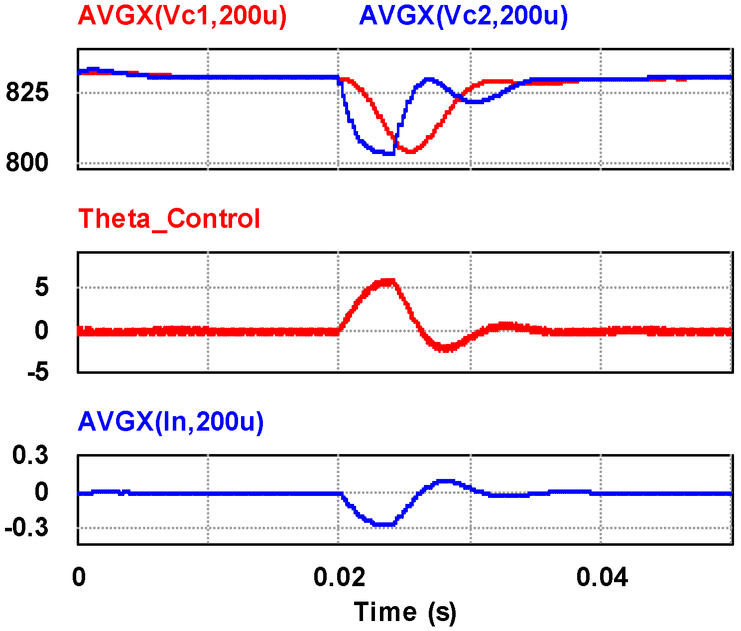
Figure 12.
Block diagram showing the capacitor voltage imbalance control.

Figure 13.
Block diagram showing key parameters and power flow from PV panels to the grid.

Figure 14.
(from top to bottom)—PV-side bridge voltage, , and current and of 1-port ML-DAB.

Figure 15.
Experimental output for ML-DAB 2-level voltage , 5-level voltage and currents through the transformers , ; where Vs = VPV = 125 V, VP = Vdc = 650 V, n = 5.71, α = 10°, β = 30°, φini = 70°.
Figure 15.
Experimental output for ML-DAB 2-level voltage , 5-level voltage and currents through the transformers , ; where Vs = VPV = 125 V, VP = Vdc = 650 V, n = 5.71, α = 10°, β = 30°, φini = 70°.

Figure 16.
(From top to bottom)—(a) ML-DAB input current and its average; (b) output current and its average; and (c) Average input and output power; efficiency = 96.42%.
Figure 16.
(From top to bottom)—(a) ML-DAB input current and its average; (b) output current and its average; and (c) Average input and output power; efficiency = 96.42%.

Figure 17.
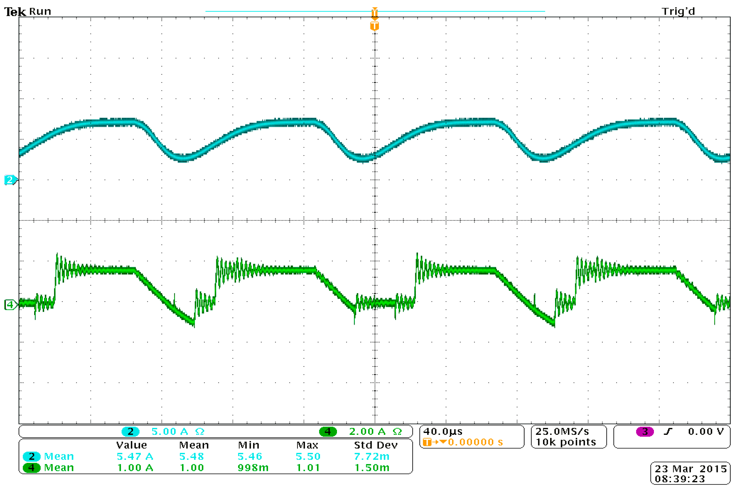
Experimental output for ML-DAB input (top–blue) and output (bottom–green) dc currents respectively.
Figure 17.
Experimental output for ML-DAB input (top–blue) and output (bottom–green) dc currents respectively.

Figure 18.
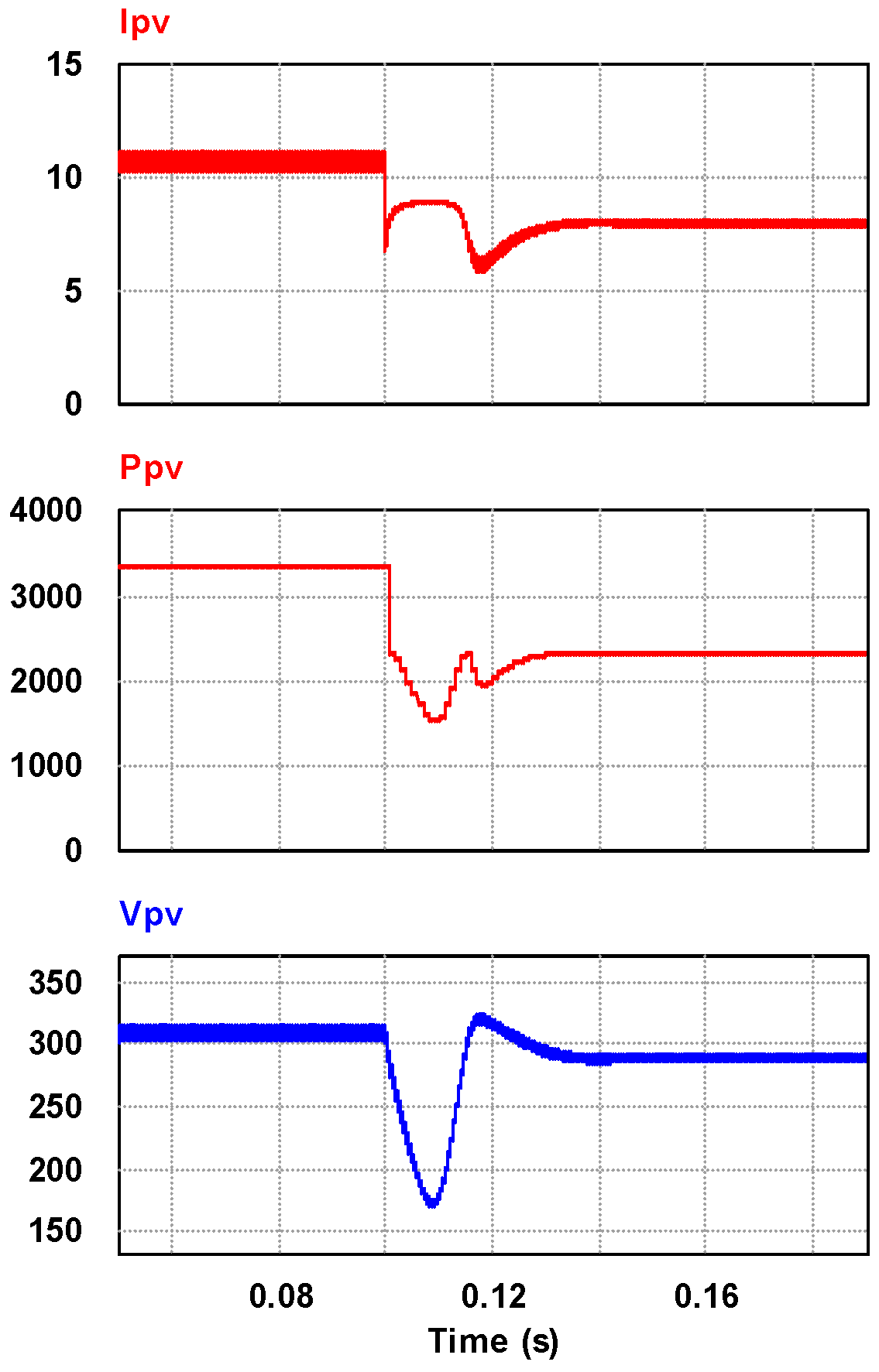
MPPT, using P&O algorithm, controls the power flow when PV generation changes due to change in insolation from 1000 W/m2 to 800 W/m2 at t = 0.1 s.
Figure 18.
MPPT, using P&O algorithm, controls the power flow when PV generation changes due to change in insolation from 1000 W/m2 to 800 W/m2 at t = 0.1 s.

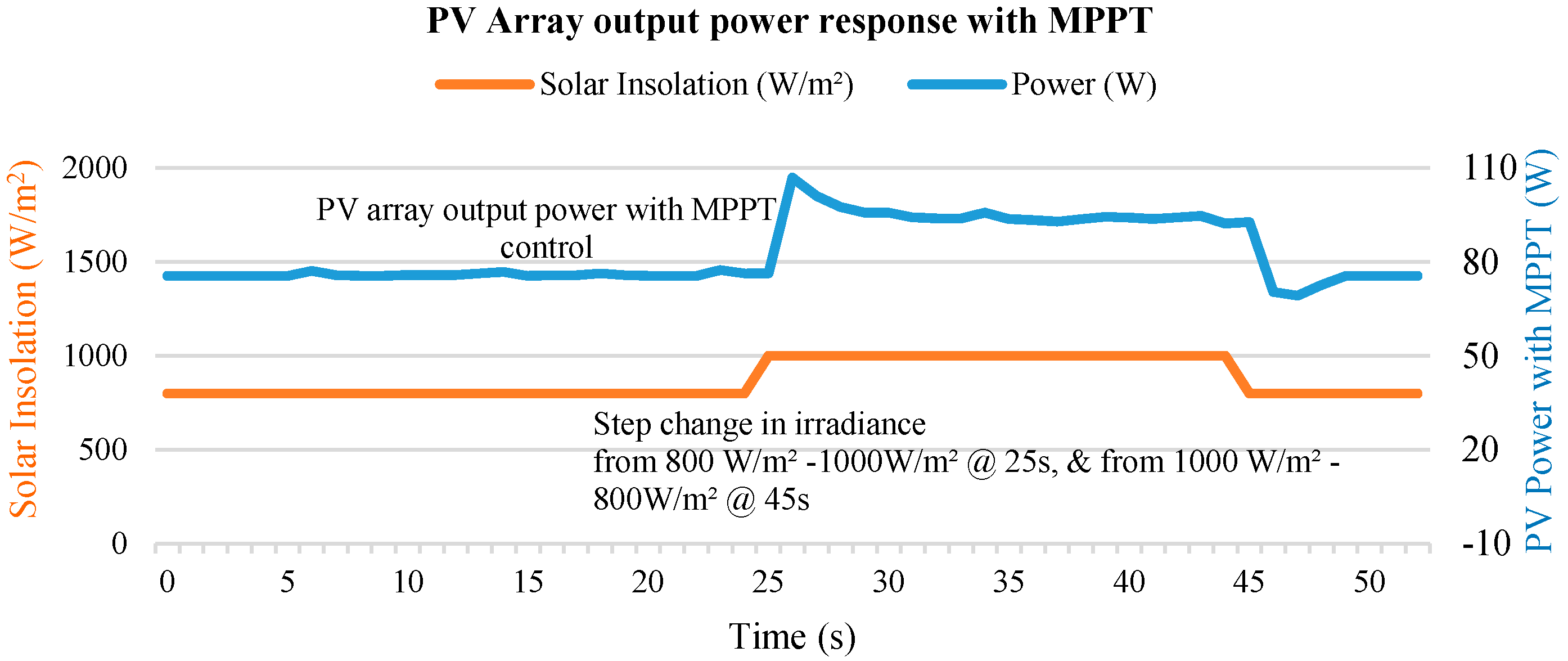
Figure 19.
The graph obtained from experimental data shows how the PV output power is controlled by the MPPT algorithm using MAGNA Power® XR200-10 PV source emulator and NI myRIO-1900®.
Figure 19.
The graph obtained from experimental data shows how the PV output power is controlled by the MPPT algorithm using MAGNA Power® XR200-10 PV source emulator and NI myRIO-1900®.

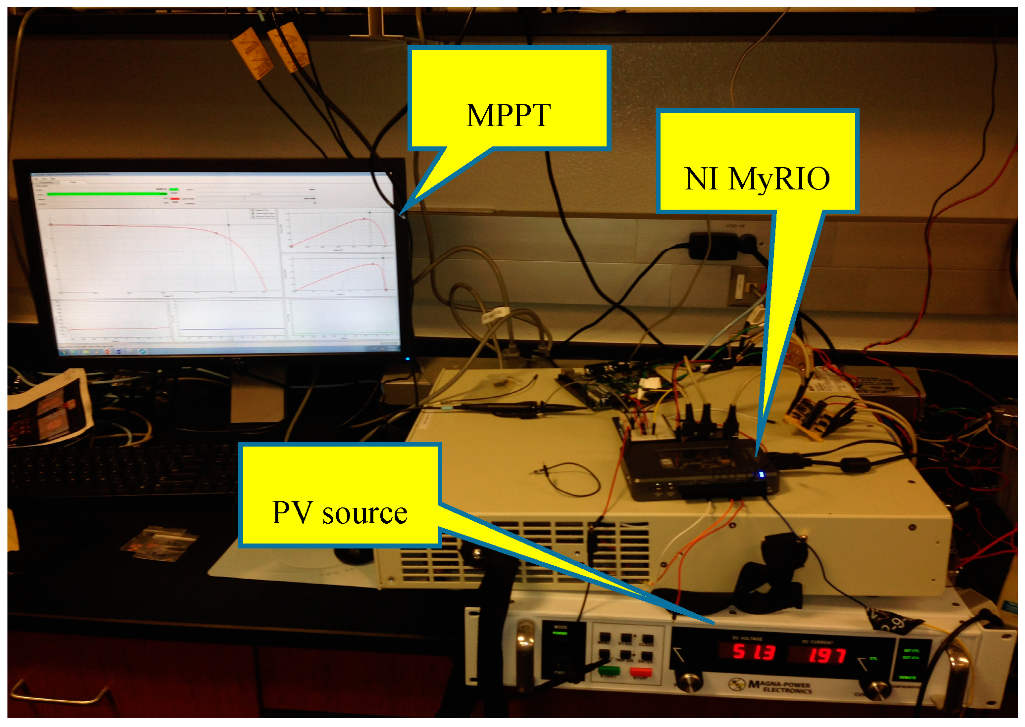
Figure 20.
Hardware setup for the MPPT control using MAGNA Power® XR200-10 PV source emulator and NI myRIO-1900® along with LabVIEW.
Figure 20.
Hardware setup for the MPPT control using MAGNA Power® XR200-10 PV source emulator and NI myRIO-1900® along with LabVIEW.

Figure 21.
(a) Response of three-phase closed loop PLL system that tracks the phase of grid voltage Va = Vm cosϴ, Vm = 2000 × V; (b) Current control of the N-port three-phase grid-connected PV converter for varying total PV input power; here PPV is dropped 10% at t = 0.4 s and increased 5% at t = 0.08 s.

Figure 22.
Based on power mismatch different dc-link voltages appear at corresponding inverter inputs.
Figure 22.
Based on power mismatch different dc-link voltages appear at corresponding inverter inputs.

Figure 23.
Despite different dc-link voltages the output phase voltages are controlled for grid synchronization.
Figure 23.
Despite different dc-link voltages the output phase voltages are controlled for grid synchronization.

Figure 24.
(From top to bottom) 5-port cascaded NPC bridge output waveform having 21 levels (THD = 5.76%), 1-port NPC bridge inverter output waveform having five levels (THD = 27.74%); THD values are obtained from simulation.
Figure 24.
(From top to bottom) 5-port cascaded NPC bridge output waveform having 21 levels (THD = 5.76%), 1-port NPC bridge inverter output waveform having five levels (THD = 27.74%); THD values are obtained from simulation.
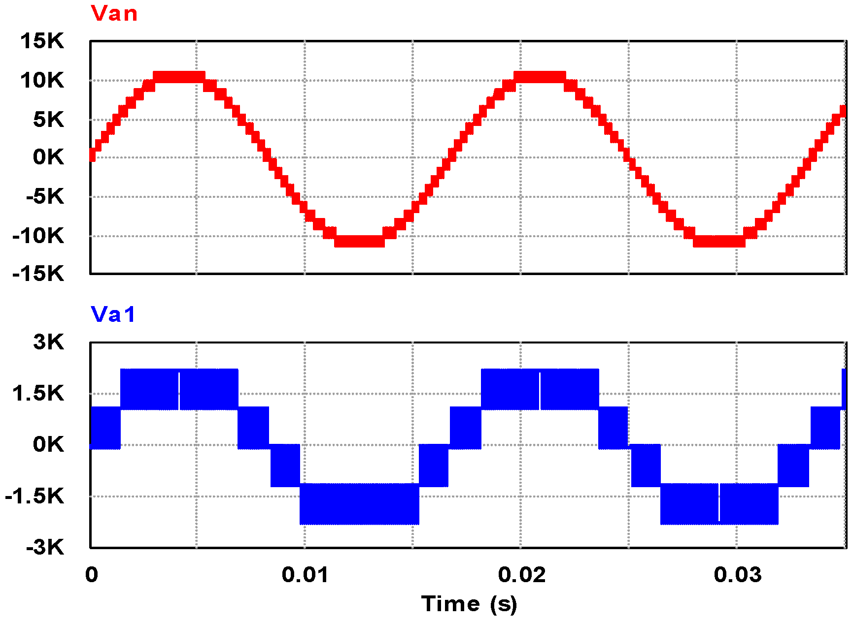
Figure 25.
Experimental Output ac voltage (60 Hz, unfiltered) from one NPC inverter (N = 1) port to producing a five (4N + 1) level , and corresponding current, through a resistive load , where .
Figure 25.
Experimental Output ac voltage (60 Hz, unfiltered) from one NPC inverter (N = 1) port to producing a five (4N + 1) level , and corresponding current, through a resistive load , where .

Figure 26.
Experimental Output ac voltage and current (60 Hz, unfiltered) when two NPC inverters (N = 2) are cascaded to produce a nine (4N + 1) level , and corresponding current, through a resistive load , where .
Figure 26.
Experimental Output ac voltage and current (60 Hz, unfiltered) when two NPC inverters (N = 2) are cascaded to produce a nine (4N + 1) level , and corresponding current, through a resistive load , where .

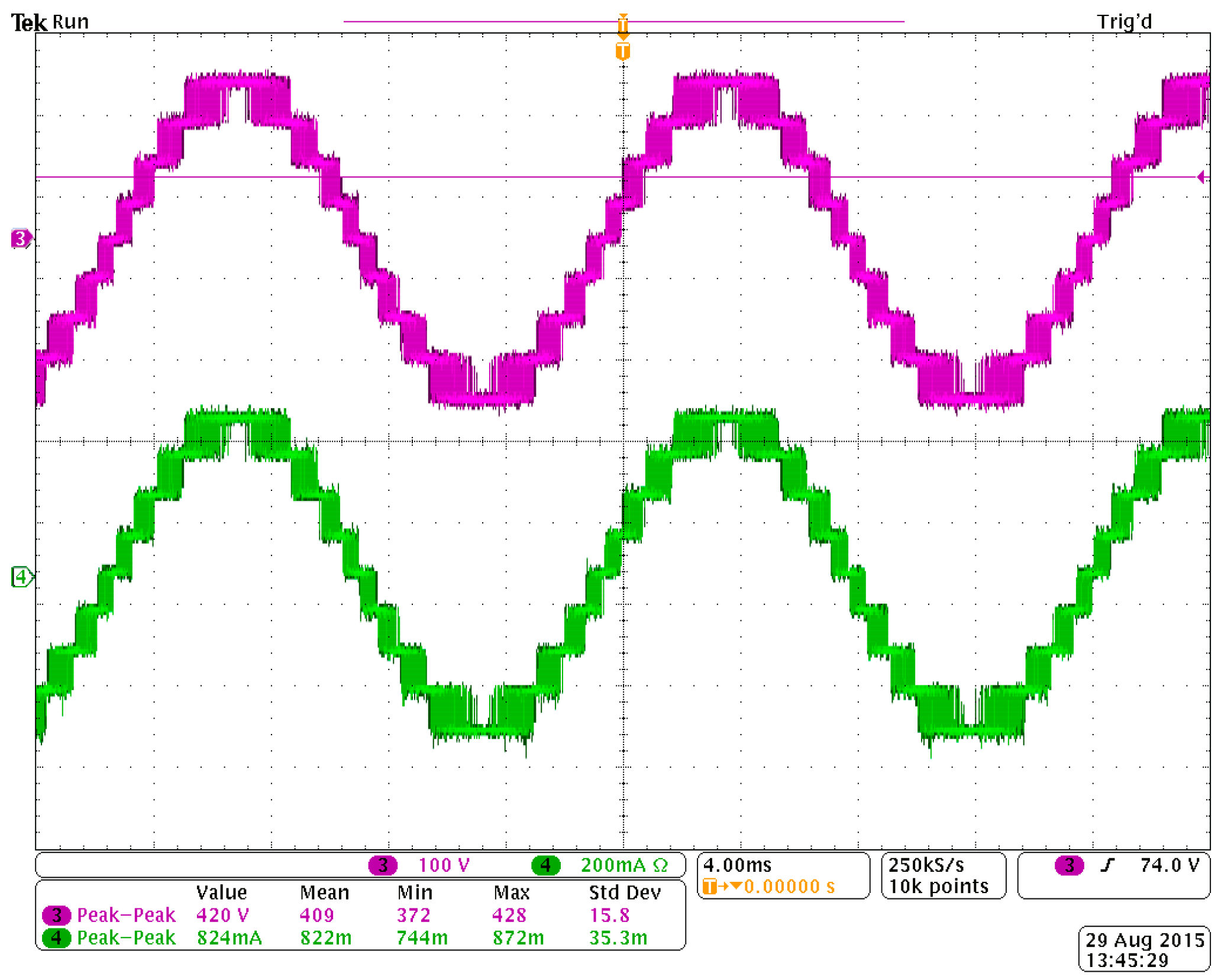
Figure 27.
Experimental output ac voltage and current (60 Hz, filtered) when two NPC inverters (N = 2) are cascaded , and corresponding current, through a resistive load , mH, where .
Figure 27.
Experimental output ac voltage and current (60 Hz, filtered) when two NPC inverters (N = 2) are cascaded , and corresponding current, through a resistive load , mH, where .

Figure 28.
Hardware setup for one port of the ML-DAB and NPC inverter with a resistive-inductive (R-L) load.
Figure 28.
Hardware setup for one port of the ML-DAB and NPC inverter with a resistive-inductive (R-L) load.


Table 1.
IGBT Selection for CHB and CNPC Inverters for N = 3 to N = 12.
| No. of Modules per Phase (N) | Assuming N-Nos. of CHB Modules per Phase | Assuming N-Nos. of CNPC Modules per Phase | ||||||
|---|---|---|---|---|---|---|---|---|
| Vdc at Each Port of CHB Inverter (V) | Required IGBT (kV) | VCE@100FIT (V) | DVUF (%) | Vdc/2 at Each Port of CNPC Inverter (V) | Required IGBT (kV) | VCE@100FIT (V) | DVUF (%) | |
| 3 | 3906 | >6.5 | - | - | 1953 | 4.5 | 2899 | 67.37 |
| 4 | 2930 | 6.5 | 3865 | 75.81 | 1465 | 3.3 | 1794 | 81.66 |
| 5 | 2344 | 4.5 | 2899 | 80.86 | 1172 | 2.5 | 1289 | 90.92 |
| 6 | 1953 | 4.5 | 2899 | 67.37 | 977 | 1.7 | 1072 | 91.14 |
| 7 | 1674 | 3.3 | 1794 | 93.31 | 837 | 1.7 | 1072 | 78.08 |
| 8 | 1465 | 3.3 | 1794 | 81.66 | 733 | 1.7 | 1072 | 68.38 |
| 9 | 1302 | 3.3 | 1794 | 72.58 | 651 | 1.2 | No FIT data available. Assuming 720 V (60% of VCES) | 90.42 |
| 10 | 1172 | 2.5 | 1289 | 90.92 | 586 | 1.2 | 81.39 | |
| 11 | 1065 | 1.7 | 1072 | 99.35 | 533 | 1.2 | 74.03 | |
| 12 | 977 | 1.7 | 1072 | 91.14 | 489 | 1.2 | 67.92 | |
Table 2.
ML-DAB Parameter Values for a 500 kW 3-phase N-port Converter.
| For a 500 kW 3-ph 13.8 kV Converter | N = 3 Ports/Phase | N = 5 Ports/Phase | N = 8 Ports/Phase | N = 12 Ports/Phase |
|---|---|---|---|---|
| Power rating of 1 ML-DAB | 55.6 kW | 33.4 kW | 20.8 kW | 13.9 kW |
| PV output voltage, Vs (for 10 or more parallel strings) | 947.7 V to 1000 V | 583.2 to 1000 V | 364.5 V to 1000 V | 291.6 V to 1000 V |
| ML-DAB output voltage, VP | 6.67 kV | 4 kV | 2.5 kV | 1.67 kV |
| HF transformer turns ratio, n = VP/Vs | 7.035 or less | 6.858 or less | 6.858 or less | 5.716 or less |
| Leakage inductor L (for minimum Vs & fs = 5 kHz) | 0.32 mH | 0.20 mH | 0.12 mH | 0.122 mH |
| ML-DAB primary IGBTs Vce | 1700 V | 1200 V | 600 V | 600 V |
| ML-DAB secondary IGBTs Vce | 4.5 kV | 3.3 kV | 1700 V | 1200 V |
Table 3.
Cost of the proposed N-port Converter based on 1 MW PV system.
| Components | Proposed N-Port Inverter |
|---|---|
| Inverters | $0.2000 |
| Transformers | Included in Inverter Cost |
| Copper Cable | $0.0252 |
| PVC conduit | $0.0085 |
| AC switchgear | $0.0337 |
| Combiners | $0.0060 |
| Concrete | $0.0059 |
| Key items above: | $0.2000 |
| Assuming rest of the project cost is same for both central and N-port inverter | |
| Overall $/watt | $1.72 |
Table 4.
(N − 1) Redundancy for a 3.34 kW Prototype design with all 1200V IGBTs assuming N = 12.
| Item Description | Each Port (for N = 12) | Each Port (for N − 1 = 11) |
|---|---|---|
| Power Rating of 1 single DAB module | 3.34 kW | 3.34 kW |
| 291.6 V | 291.6 V | |
| 1667 V | 1820 V | |
| DAB high frequency transformer’s turn ratio, n | 5.716 | 5.716 |
| 11.43 A | 10.48 A | |
| 2 A | 1.835 A | |
| Phase-shift among CNPC inverter outputs | (N/180) =15° | ((N − 1)/180) = 16.37° |
Table 5.
Hardware component specification for one port of the proposed converter.
| Hardware Component | Item Description | Quantity per Port | |
|---|---|---|---|
| PV source Emulator | MAGNA Power XR200-10 | 1 | |
| Voltage transducer | SCK-MU-1500V | 1 | |
| Current Transducer | CR5410-20 | 1 | |
| MPPT controller | NI myRIO-1900®, LabVIEW | 1 | |
| ML-DAB primary bridge | IGBT (Dual) | Infineon FF100R12YT3 | 2 |
| Capacitor | 550 V, 1200 µF | 1 | |
| High frequency transformer | Core Material | Metglass amorphous alloy 2605SA1 AMCC-125 | 1 |
| Winding turns ratio | 89:509 | - | |
| Winding wire (Round Litz Wire) | Primary: AWG 12-259/36, Secondary: AWG 20-38/30 | - | |
| ML-DAB secondary NPC bridge | IGBT (Dual) | Infineon FF100R12YT3 | 4 |
| Capacitor | 1200 V, 100 µF | 2 | |
| Clamping Diode | IXYS DSEP30-12AR | 4 | |
| NPC Inverter bridge | IGBT (Dual) | Infineon FF100R12YT3 | 4 |
| Clamping Diode | IXYS DSEP30-12AR | 4 | |
| Gate pulse generator | ML-DAB&Inverter | NI myRIO-1900®, LabVIEW | 1 |
| Load at output | R-L load | R = 500 Ω, L = 500 mH | 1 |
| Waveform measurement | Signal Oscilloscope | Tektronix MSO-4034 | 1 |
© 2017 by the authors. Licensee MDPI, Basel, Switzerland. This article is an open access article distributed under the terms and conditions of the Creative Commons Attribution (CC BY) license (http://creativecommons.org/licenses/by/4.0/).
Share and Cite
MDPI and ACS Style
Duman, T.; Marti, S.; Moonem, M.A.; Abdul Kader, A.A.R.; Krishnaswami, H. A Modular Multilevel Converter with Power Mismatch Control for Grid-Connected Photovoltaic Systems. Energies 2017, 10, 698. https://doi.org/10.3390/en10050698
AMA Style
Duman T, Marti S, Moonem MA, Abdul Kader AAR, Krishnaswami H. A Modular Multilevel Converter with Power Mismatch Control for Grid-Connected Photovoltaic Systems. Energies. 2017; 10(5):698. https://doi.org/10.3390/en10050698
Chicago/Turabian StyleDuman, Turgay, Shilpa Marti, M. A. Moonem, Azas Ahmed Rifath Abdul Kader, and Hariharan Krishnaswami. 2017. "A Modular Multilevel Converter with Power Mismatch Control for Grid-Connected Photovoltaic Systems" Energies 10, no. 5: 698. https://doi.org/10.3390/en10050698
Note that from the first issue of 2016, this journal uses article numbers instead of page numbers. See further details here.