1. Introduction
The market for energy storage systems is dynamic and experiencing accelerated growth [
1]. This is because several power systems require, for their correct operation, energy storage devices either as a primary source or backup source, e.g., SLI systems (starting, lighting, ignition), electrical systems in the automotive industry, portable electronic devices, micro-grids, systems in the marine sector, medical devices, seismic devices, uninterruptible power supply (UPS), forklift equipment, and telecommunication equipment, among others. Therefore, finding cost-effective methods to store energy is of importance. There are currently many technologies for storing energy, including electro-chemical, mechanical, thermal, hydraulic and pneumatic technologies [
2,
3,
4,
5,
6,
7]. Among the electro-chemical technologies, the most well-known solutions are ultracapacitors, lithium ion batteries (Li-ion), lead-acid batteries and flow batteries [
2,
8,
9,
10].
Batteries have some advantages with respect to other storage systems, namely, higher charge efficiency, responsiveness and simplicity of installation. For example, Li-ion batteries exhibit high charge efficiency, near 99%, and high energy efficiency, between 86% and 99%, depending on the charge and discharge C-rate [
11]. Conversely, other power sources, such as fuel cells, have lower efficiencies near 60% [
12]. Moreover, a battery is always ready to deliver power without warm-up, whereas a fuel cell requires some minutes before producing power. Due to the diversity of applications that require batteries, the market is very dynamic, e.g., lead-acid batteries are by far the most important market, near 90%, mainly in SLI, telecommunications, transport vehicles and UPS. However, Li-ion batteries have the highest growth and major part of industry investments, taking markets such as cellular phones, notebooks, automobiles, camcorders, e-bikes, and so forth [
1].
The forecasts for 2010–2025 show that the compound annual growth rate (CAGR) of the battery market will be 10%, being dominated by lead-acid batteries, but with a growth near 150% in the market of Li-ion batteries due mainly to electric vehicles (EVs) [
1]. However, there are new applications for Li-ion batteries, such as UPS, telecommunications, forklifts, medical devices, residential ESS (energy storage system), and grid ESS with a CAGR estimate of 15% [
1].
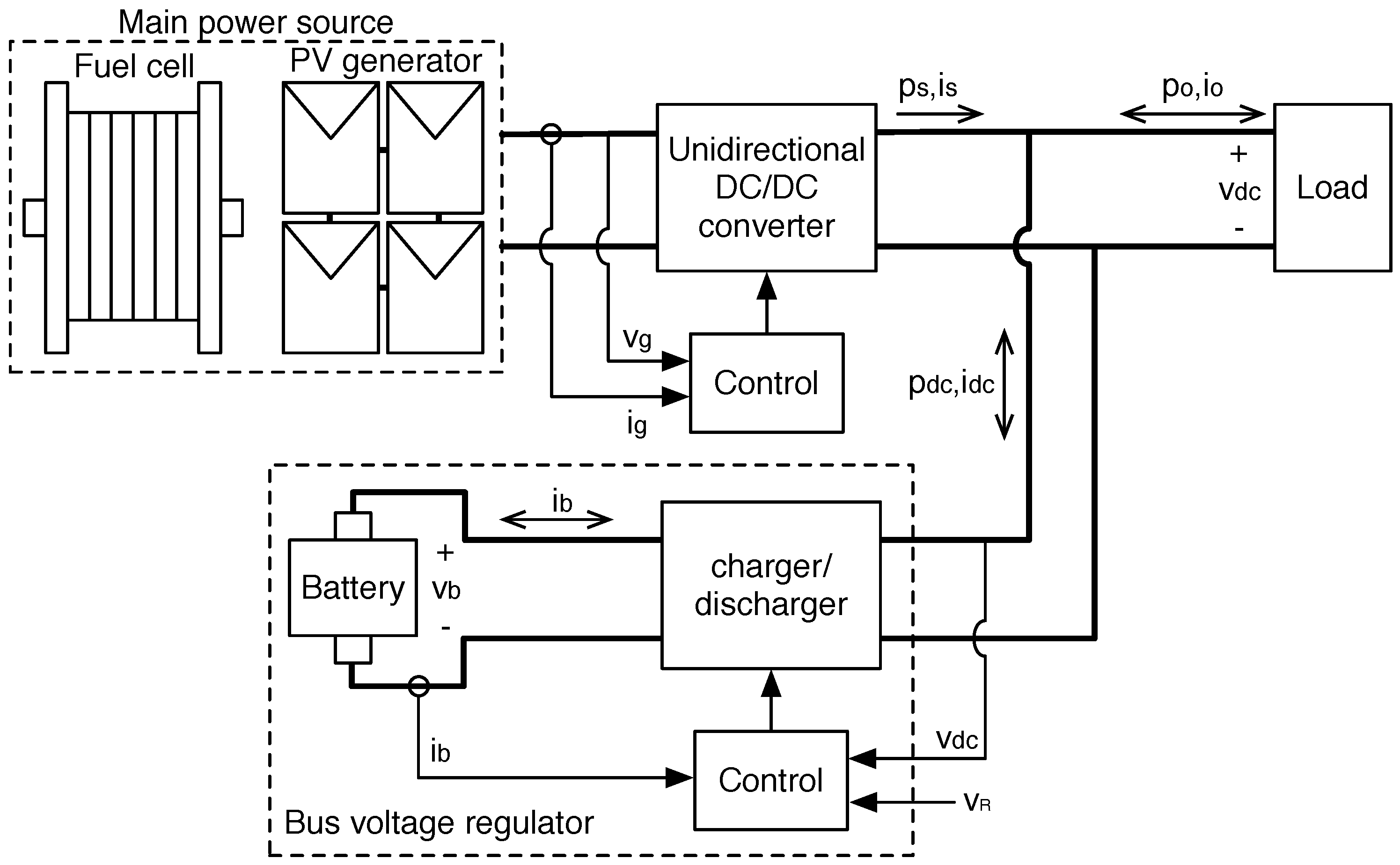
Another important application in which batteries are extensively used is the construction of stand-alone renewable power systems, which are common solutions for remote energy generation and urban/distributed energy systems for pollution reduction [
13,
14]. A common structure of such power systems based on renewable generators and batteries is presented in
Figure 1 [
15,
16,
17,
18,
19,
20,
21,
22]. Such an architecture has a renewable energy source as the main energy generator, e.g., photovoltaic modules or fuel cell, interacting with a unidirectional DC/DC converter that is responsible for optimizing the source operating conditions. The output of the DC/DC converter is connected to a DC bus that is regulated by a charger/discharger power converter, which also interfaces the battery with the DC bus. The charger/discharger converter is controlled to regulate the DC bus voltage within safe limits and simultaneously impose a given energy flow between the battery and the DC bus. Due to safety implications for the source and load, there are many research papers focused on regulating the DC bus voltage using charger/discharger converters: some of them are based on linear control [
16,
23,
24,
25,
26], others are based on intelligent control [
13,
27,
28,
29,
30,
31,
32], and others are based on non-linear control strategies [
15,
17,
18,
19,
20,
21,
22].
In particular, sliding-mode controllers (SMCs) have been widely used for this application to ensure global stability, robustness to parameter tolerances, higher bandwidth compared with classical linear controllers [
17,
22,
33], and reduced implementation cost and complexity compared with intelligent controllers [
31,
34]. For example, the work reported in [
15] proposed an SMC for the charger/discharger converter of the stand-alone power system described in
Figure 1. The sliding-surface is formed by the battery current and a PI structure processing the DC bus voltage error. In this solution, the design equations and existence conditions of the sliding mode depend on the converter duty cycle; hence, the parameters of the sliding surface must be adjusted on-line. Such adaptiveness guarantees the global stability of the system, which is an important advantage over classical solutions based on linear control. However, the rejection of bus current perturbations must be improved by introducing additional terms into the surface, as will be discussed in
Section 2 and
Section 3.
Another solution based on SMC was reported in [
21]. That work was aimed at controlling a buck-boost charger/discharger converter with a cascade structure: an outer voltage loop based on a PI structure defines the reference of an inner current loop based on an SMC, in which the sliding surface is formed by the inductor current error. This solution is applied in electric vehicles.
Similarly, the work reported in [
18] proposed a cascade control of a DC/DC converter based on a half-bridge bidirectional topology. In this case, the current control is designed with a fixed-frequency SMC to reduce electromagnetic interferences (EMI). In [
20], a cascade control for a battery charger of an electric vehicle was proposed, but in this case, the converter is a unidirectional implementation. In that work, the inner inductor current control is designed with a discrete-time SMC, while the outer control loop calculates the current reference such that a power factor correction (PFC) stage regulates the DC-link voltage, and simultaneously, the current reference of buck-type cells is determined depending on the state of charge (SOC) of the battery. Another SMC for controlling a bidirectional DC/DC converter used to interface a parallel-connected hybrid energy storage system was proposed in [
22]. This system is formed by a vanadium redox battery, a supercapacitor and a renewable power source. Moreover, in that work, the sliding-surface is similar to the one introduced in [
15], but without any adaptability to compensate for the duty cycle variation.
In [
16], the problem of a multi-source power sharing strategy within electric vehicles was addressed using an upper-level control (control objectives) based on a robust linear parameter-varying (LPV) controller [
35] and a lower-level control based on a classical PI current control. In this solution, the DC bus voltage regulation is part of the control objectives, which enables calculating the PI current control of a bidirectional DC/DC power converter driving the battery; hence, the hardware structure is similar to that shown in
Figure 1. Meanwhile, the battery charger circuits proposed in [
17,
19] use unidirectional DC/DC converters, regulated with non-linear controllers, to interface the PV panels and the batteries.
The solution proposed in this paper is aimed at providing a tight regulation of the DC bus voltage in a stand-alone power system based on renewable energy sources to ensure a safe operation. This objective is fulfilled by designing a sliding-mode controller for the battery charger/discharger to regulate the bus voltage under any power flow condition; however, in contrast to the solutions previously discussed [
15,
16,
22,
26], this new solution proposes including the DC bus current in the sliding surface to improve the disturbance rejection. Moreover, the proposed solution does not use a cascade control structure; hence, a single controller defines the MOSFET state based on the measurements of the battery current and bus voltage and current. This characteristic simplifies the controller implementation and reduces the cost.
The remainder of this paper is organized as follows. In
Section 2, the background of the proposed solution is presented.
Section 3 describes the design of the proposed sliding-mode controller and the analysis of the transversality, reachability and equivalent control conditions.
Section 4 addresses the design of the sliding-mode dynamics to ensure a tight regulation of the DC bus voltage. Then,
Section 5 presents the implementation of the control law and the synthesis of the switching surface.
Section 6 and
Section 7 present a design example and the simulation and experimental results. Finally, the conclusions close the work.
2. Background of the Proposed Solution
The classical solution to control a battery charger/discharger is based on an inner current loop and an outer voltage or power loop. The current loop has two main purposes: reduce the order of the system to simplify the controller design and reject fast current perturbations generated in the DC bus, for example, compensate changes in the power produced by the generator (e.g., sunlight increase/decrease in a PV system) or in the power requested by the load. The use of this structure is reported in the battery charger/discharger applications recently published in [
36,
37].
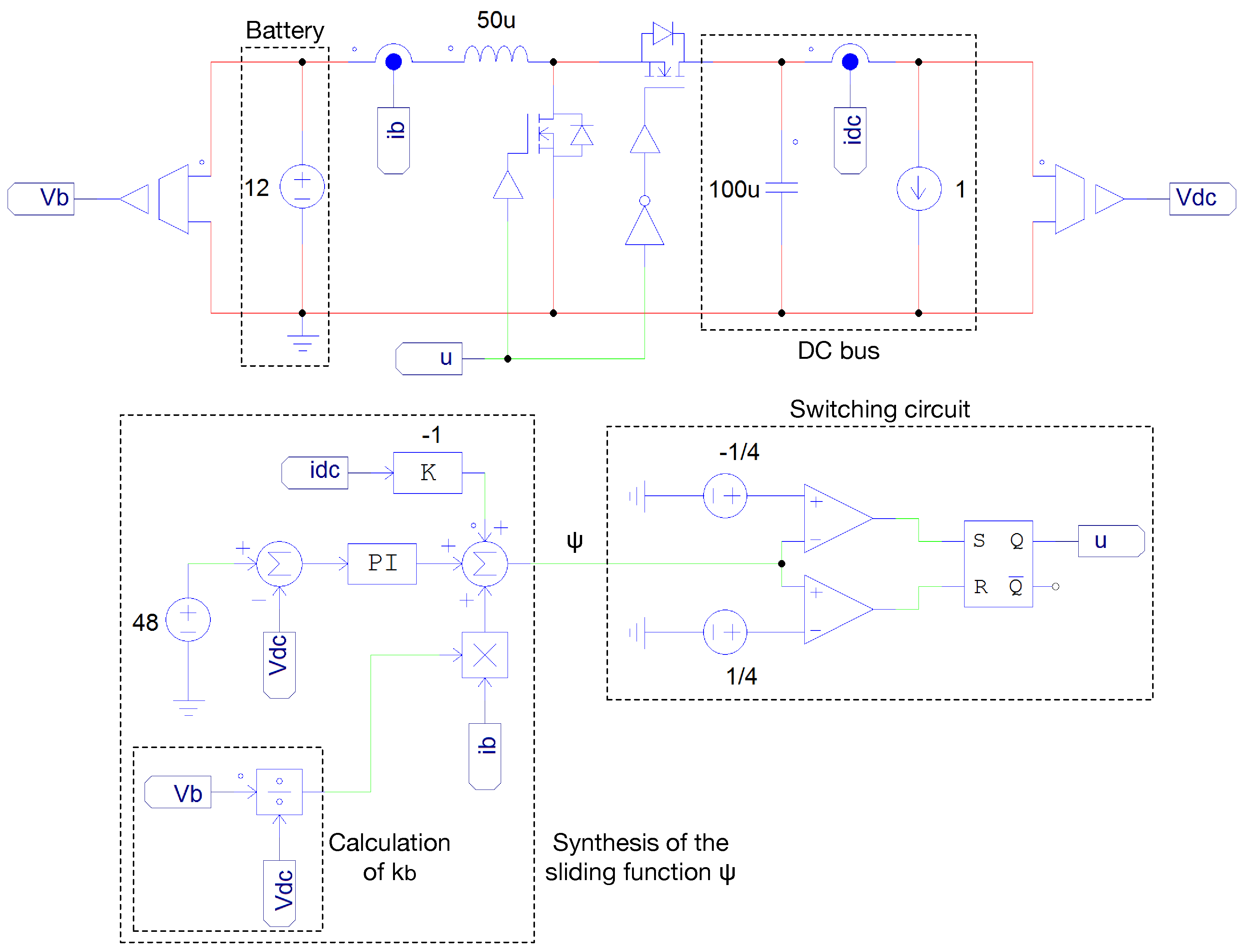
A widely used battery charger/discharger DC/DC converter is presented in
Figure 2, which is based on a bidirectional boost (buck) converter [
38]. Moreover, this figure also illustrates a classical cascade current-voltage control structure, in which the current controller acts on the MOSFET signal
u directly (e.g., sliding-mode, peak current, valley current controllers) or using a PWM (e.g., average current control). This structure is used to avoid the non-minimum phase condition exhibited by the transfer function between the DC bus voltage and the converter duty cycle. This is achieved by controlling the inductor current, i.e., the battery current, which exhibits a minimum phase transfer function with respect to the duty cycle. Then, the inductor is modeled as a current source to provide a minimum-phase first-order transfer function between the DC bus voltage and the current reference; hence, a linear controller can be used to regulate the bus voltage. However, this strategy requires a narrow bandwidth in the voltage loop to ensure the validity of the current source approximation. This is the main drawback of the cascade structure: the bandwidth of the voltage controller is between 5 and 10 times smaller than the current loop [
39,
40,
41]. Hence, the controller speed is constrained, which reduces its ability to compensate fast perturbations.
The cascade structure has also been used to control the power flow between the battery and the DC bus. This case was reported in [
38], which uses an inner control loop to regulate the battery current and an outer control loop to regulate the DC bus energy. Note that the circuit presented in
Figure 2 has an equivalent behavior: in a power system with a regulated DC bus, similar to the one presented in
Figure 1, the difference between the load power and power provided by the main generator is stored/supplied in the DC bus capacitor. Therefore, the battery charger/discharger must be controlled to regulate the DC bus voltage, which forces transferring that power difference from the DC bus capacitor into the battery. In this case, if the DC bus voltage is increased by a positive power difference between the generator and load power profiles, then the charger/discharger transfers that energy from the DC bus to the battery; similarly, if the DC bus voltage is decreased by a negative power difference between the generator and load power profiles, then the charger/discharger extracts that energy from the battery to supply the DC bus.
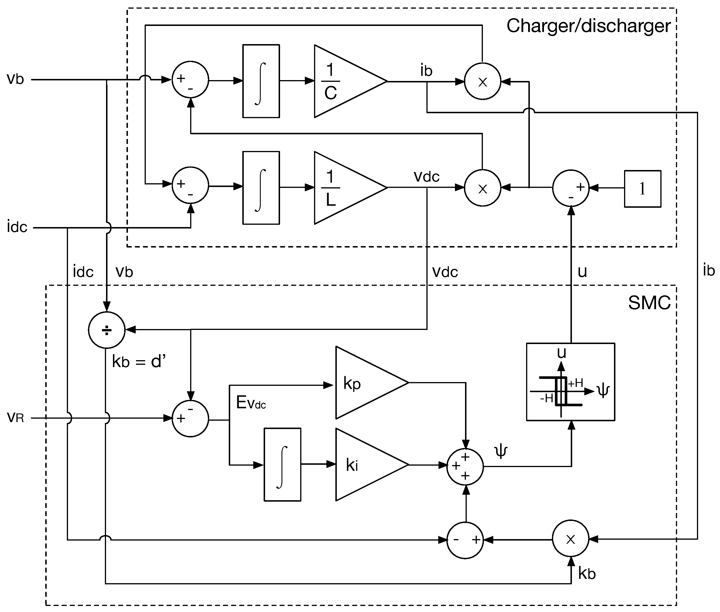
To avoid the bandwidth constraint imposed by the cascade solution, the work reported in [
15] uses a unified sliding-mode controller for the charger/discharger, as illustrated in
Figure 3. Since this solution does not require any model approximation, the voltage control can be designed with the highest bandwidth possible, which provides a faster response compared with the cascade solution. Therefore, the unified controller has higher speed, which improves its ability to compensate perturbations. Moreover, since the SMC is designed using the non-linear model of the DC/DC converter, it ensures the system stability and desired performance in any operating conditions, which provides a safe operation in the entire operation range.
The SMC designed in [
15] is based on the sliding function
and sliding surface
presented in (
1) and (
2), respectively. In these expressions,
represents the battery current, which is equal to the inductor current as observed in
Figure 2 and
Figure 3;
represents the DC bus voltage; and
represents the desired bus voltage, i.e., the reference value. Moreover,
and
are parameters designed to impose a desired dynamic response on the DC bus voltage.
However, both the cascade and unified control solutions have a main disadvantage: the controller is not able to instantaneously identify a perturbation in the bus current; therefore, the controller reacts to the perturbation in the bus voltage, which causes large voltage disturbances. For example, in the cascade solution, the current controller acts on the battery current only when the voltage (or power) controller detects a perturbation in the bus voltage (or power); hence, the compensation provided by the current controller is delayed, which in turn delays the voltage (or power) compensation. The same behavior is observed in the results of the unified SMC reported in [
15].
Figure 4 presents the simulation of the unified SMC reported in [
15], which was designed to provide a bus voltage equal to 48 V. The controller must provide a maximum voltage deviation of 2 V for current transients in the bus up to 1 A. The simulation shows a correct behavior up to 20 ms, when a 3 A current transient occurs in the DC bus, causing a voltage drop to almost 45 V (3 V).
The magnified area of the simulation (from 19.8 ms to 21.0 ms) also reveals the reason for the large voltage deviation caused by current transients: the change in the bus current must be compensated by the battery current, which due to power balance corresponds to a theoretical battery current of
. However, as observed in the magnified region of the figure, the battery current imposed by the controller is considerably slower than the theoretical battery current; hence, the current difference must be provided by the bus capacitor, producing a voltage drop. This behavior is unavoidable in the structure of
Figure 3 because, as observed in the magnified region of
Figure 4, the battery current is defined by the error between the bus voltage and the reference. Therefore, the battery current changes only when a deviation in the bus voltage occurs.
This undesired behavior can be removed by introducing the measurement of the bus current into the control scheme, which will enable the controller to impose a faster change in the battery current. The next section proposes a new sliding-mode controller based on this concept.
3. Proposed Sliding-Mode Controller
With the aim of improving the current disturbance rejection for the charger/discharger, the control structure proposed in
Figure 5 considers the measurement of the bus current. Moreover, the controller must be designed to take advantage of this new information. In addition, since the charger/discharger must be controlled in both positive and negative power flows by the same controller and because the bandwidth of the system must be set as high as possible, i.e., no linearization processes involved, the proposed controller is based on sliding-mode theory.
The proposed SMC is based on the sliding function
and surface
presented in (
3) and (
4), respectively. This new surface includes the bus current
, a new parameter
weighting the battery current
, the error between the bus voltage
and the reference value
weighted by the parameter
, and the integral of the error between
and
weighted by the parameter
. Then, the parameters
,
and
must be designed to impose a desired dynamic response on the bus voltage.
The viability of implementing an SMC based on the surface
presented in (
4) depends on three conditions [
42]: transversality, reachability and equivalent control. These conditions are analyzed in the following subsections.
3.1. Converter Model and Sliding Function Expressions
The first step in evaluating the viability of the sliding-mode controller is to provide an explicit expression for the sliding function derivative, which also requires a switched model for the DC/DC converter [
43].
The converter dynamic behavior is described in terms of the switched differential equations presented in (
5) and (
6), where
L,
C and
u represent the inductance, capacitance and MOSFET control signal, respectively.
From the charge and flux balances in the capacitor and inductor, respectively [
44], the steady-state battery and bus voltages are related by (
7), where
d represents the converter duty cycle. Similarly, the steady-state battery and bus currents are related by (
8).
The derivative of the sliding function (
3) is presented in (
9), which considers the reference value to be constant, i.e.,
. This assumption is valid since a DC bus is commonly controlled to provide a constant voltage [
15,
26]. In fact, the objective of the proposed controller is to keep the bus voltage constant even under transients of the load current (or power). Finally, the explicit expression (
10) for the sliding function derivative is obtained by substituting (
5) and (
6) into (
9).
3.2. Transversality Condition
The transversality condition analyzes the ability to act on the sliding function to reach the sliding surface. This condition is formalized in (
11), which ensures that the converter control signal
u is present in the sliding function derivative [
45]. If the transversality condition (
11) is fulfilled, then the SMC is able to modify the sliding function trajectory by changing its derivative to reach the surface. Otherwise, the SMC output has no effect on the sliding function trajectory, and the bus voltage will not be controllable.
By substituting (
10) into (
11), the transversality expression is obtained, as presented in (
12). This expression can be equal to zero since the battery current is negative in the charging stage. Therefore, such an expression must be analyzed to define the constraints that ensure the fulfillment of the transversality condition (
11).
Another important implication of the transversality value is the definition of the reachability conditions, which are imposed by the transversality sign [
42], as will be discussed in the following subsection. In addition, these reachability conditions impose the control law of the MOSFETs. Therefore, to ensure a consistent implementation circuitry for the sliding-mode controller, the transversality must exhibit the same sign in any condition. This is addressed by forcing expression (
12) to exhibit a positive sign in the charging (
), stand-by (
) and discharging (
) stages. A positive sign is selected rather than a negative sign to simplify the implementation.
The constraints that ensure a positive sign for the transversality in the three possible stages of the charger/discharger are as follows:
Stand-by stage (
): since
L and
are positive quantities, the parameter
must be set as a positive quantity, as reported in (
13).
Charging stage (
): since
L,
C,
and
are positive quantities, the parameter
must be set as a negative quantity, as reported in (
14).
Discharging stage (
): since
L,
C,
and
are positive quantities, the parameter
must fulfill the constraint presented in (
15) to ensure the positive sign of the transversality.
In conclusion, the constraints reported in (
16) must be fulfilled to ensure that the transversality condition (
11) is satisfied and to simultaneously impose a positive sign of (
12) for any operating conditions.
3.3. Reachability Conditions
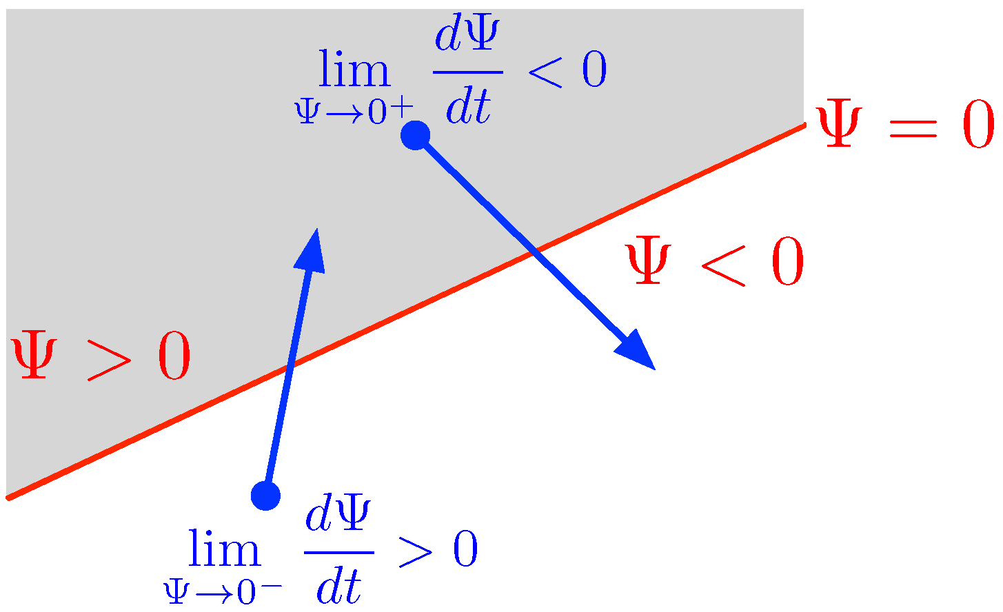
The reachability conditions analyze the ability of the system to reach the desired surface
. This concept is illustrated in
Figure 6: when the system operates under the surface, which means a negative value of the sliding function (
, the derivative of the sliding function must be positive to enable the system to reach the surface
. Similarly, when the system operates over the surface, which means a positive value of the sliding function (
, the derivative of the sliding function must be negative to enable the system to reach
. Then, the continuous switching between positive and negative derivatives of
around
creates the sliding mode [
42].
However, the sign of the derivative of
depends on the transversality sign:
implies that a positive value of
u (
) causes a positive change in
. Similarly,
implies that
causes a negative change in
. Therefore, since this work has imposed a positive sign of the transversality in (
16), the following conditions must be fulfilled to ensure the reachability of the surface:
Substituting the expression of
presented in (
10), evaluated for
, into (
17) leads to (
19). This inequality enables establishing a restriction that must be fulfilled to ensure the surface reachability.
By using the charge and flux balance principles presented in (
7) and (
8), expression (
19) is rewritten as constraint (
20), which defines the relation between the maximum derivative of
and the parameter
that ensures the existence of the sliding mode. In this expression, the terms
and
are positive, where the latter one is the transversality (
12). However, the term
could be positive or negative; hence, the worst case (lower value) to be evaluated corresponds to the condition in which
has an opposite sign to
.
A particular case for (
20) occurs for a step perturbation in the DC bus current, which is the fastest (and strongest) perturbation possible: in this case, restriction (
20) is not fulfilled in the very short time
in which the step occurs because
, but after that short time, the current is almost constant, i.e.,
. Considering that
Section 4 will demonstrate that
must be negative (
36) for stability reasons, expression (
20) is modified to define the maximum magnitude of
that ensures the reachability of the surface, presented in (
21), which corresponds to the most restrictive case:
with opposite sign to
, i.e.,
.
The other case
produces the inequality provided in (
22), which is always fulfilled.
To summarize, constraint (
21) provides the maximum magnitude of
to ensure reachability when the bus voltage is lower than the reference, i.e.,
.
The second reachability condition (18) is also analyzed by evaluating the expression of
provided in (
10) for
:
Using the charge and flux balance principles presented in (
7) and (
8), expression (
23) is rewritten as constraint (
24), which defines the relation between the minimum derivative of
and the parameter
that ensures the existence of the sliding mode. In this expression, the term
is negative, and the term
is positive. However, the term
could be positive or negative; hence, the worst case (higher value) to be evaluated corresponds to the condition in which
has the same sign as
.
In the particular case for (
24) with a step perturbation in the bus current, the restriction is not fulfilled in the very short time
in which the step occurs because
, but after that short time, the current is almost constant, i.e.,
. Considering that
is negative, expression (
24) is modified to define the maximum magnitude of
that ensures the reachability of the surface, presented in (
25), which corresponds to the most restrictive case:
with the same sign as
, i.e.,
.
The other case
produces the inequality in (
26), which is always fulfilled.
To summarize, constraint (
25) provides the maximum magnitude of
to ensure reachability when the bus voltage is greater than the reference, i.e.,
.
In conclusion, the system is able to reach the surface
when the restrictions presented in (
20), (
21), (
24) and (
25) are fulfilled.
3.4. Equivalent Control
The equivalent control condition analyzes the saturation of the control signal to ensure that the system is always in a closed-loop state. The equivalent control corresponds to the average value
of the binary control signal
u within the switching period
, which is reported in (
27). Then, the equivalent control condition imposes that
must be constrained within the possible values of
u [
42,
45], which in DC/DC converters are
and
. The equivalent control condition is formalized in (
28).
It is evident that the equivalent control (
27) is equal to the converter duty cycle, i.e.,
. Therefore, fulfilling the equivalent control condition (
28) prevents saturation of the duty cycle, which ensures that the controller is continuously acting on the system to compensate perturbations. Otherwise, if the duty cycle is saturated, then the converter will operate without any control.
The equivalent control condition assumes the existence of the sliding mode, which ensures that the sliding function is in the sliding surface and its trajectory is parallel to the surface [
42]. These conditions are formalized as follows:
The expression for
is obtained using the following procedure: first, the switched differential Equations (
5) and (
6) are averaged within the switching period; then, the expression for
in (
9) is recalculated based on these averaged expressions, changing
u by the equivalent control
. Finally,
is obtained by evaluating (30) with the averaged version of
. The expression of
for the proposed SMC is presented in (
31).
Finally, evaluating the equivalent control condition (
28) considering the expression for
presented in (
31) leads to the same restrictions provided in (
20), (
21), (
24) and (
25). This result is expected since in [
42], it was demonstrated that any SMC for DC/DC converters that fulfills the reachability conditions also fulfills the equivalent control condition. In any case, this subsection is devoted to demonstrating that the proposed sliding-mode controller avoids duty-cycle saturation.
3.5. Summary
The proposed sliding-mode controller based on the sliding function (
3) and sliding surface (
4) must fulfill the constraints reported in (
16), (
20), (
21), (
24) and (
25) to ensure the sliding function controllability, surface reachability and non-saturation of the duty cycle. Moreover, the existence of the sliding mode guarantees operation of the system within the sliding surface (
29) and forces its trajectory to be parallel to the surface (30). These conditions ensure global stability of the system [
46].
4. Design of the Sliding-Mode Dynamics
The sliding-mode dynamics are imposed with the parameters
,
and
. From the sliding function (
3), it is observed that selecting parameter
equal to the complement of the converter duty cycle, as provided in (
32), forces the term
to become equal to the average current in the bus capacitor
(within the switching period
), which only disregards the switching ripple. This value for
fulfills the restriction imposed in (
16) and simultaneously enables combining both
and
measurements into a single current value to simplify the mathematical analysis.
The sliding-mode controller imposes the closed-loop dynamics (
29) and (30), which are both linear for the selected sliding function. By using the
value presented in (
32), condition (
29) becomes the expression in (
33). Since this equation is also linear, the equivalent dynamics are expressed in the Laplace domain as reported in (
34). Finally, the closed-loop transfer function
between the DC bus voltage and the reference value is provided in (
35).
Considering that
is negative (
16), transfer function (
35) indicates that a negative
value is required to ensure stable sliding-mode dynamics, i.e., negative closed-loop poles. This condition is formalized in (
36).
The following subsections address the design of to obtain a desired dynamic response in the DC bus voltage.
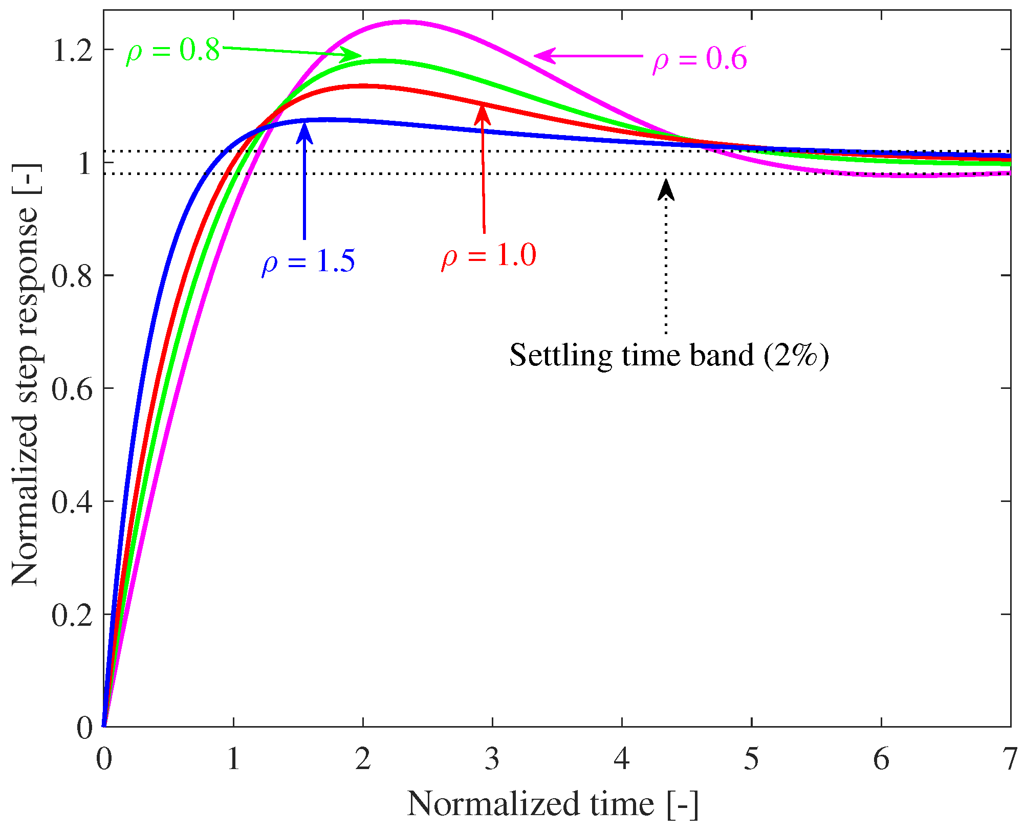
4.1. Selection of the Type of Dynamic Response
The two poles of the transfer function
can be designed in three different ways depending on the damping ratio
: complex-conjugate (
), real and equal (
), or real and different (
). To study the dynamic behavior of the closed-loop system depending on the type of damping ratio,
is rewritten as shown in (
37), where
represents the natural frequency of the system. To exclusively analyze the effect of the damping ratio, the transfer function is normalized in terms of the natural frequency using the normalized Laplace variable
as in (
38).
Figure 7 shows the normalized dynamic response of
to a step perturbation for different damping ratios: the higher the damping ratio is, the lower is the maximum overshoot. However, also note that
produces an overshoot equal to 13.5%, and even
produces an overshoot equal to 7.6%. Therefore, to ensure a low overshoot, it is necessary to design
with
, which requires the design of two real and different poles.
The results presented in
Figure 7 are valid for any natural frequency; hence, it is a general analysis. Finally, in the following subsections, the two real poles are designed to impose a given maximum overshoot and settling time, both defined by the load requirements.
4.2. Design of the Maximum Overshoot
It is important to limit the maximum (and minimum) DC bus voltage caused by perturbations in the bus current. These constraints depend on the voltage levels required by the load for normal operation. Therefore, a maximum overshoot must be imposed on .
The overshoot is designed in terms of the poles of
and considering a step perturbation, which is the strongest (and fastest) perturbation possible. For this analysis,
is expressed in terms of the two real poles
and
of the characteristic equation presented in (
39). The objective of this subsection is to find an expression for
and
that limits the overshoot
under a given maximum value.
The step response
in the Laplace domain is calculated in (
40), and the time response to a unitary step is presented in (
41). This time-domain waveform will be used to design
and
.
To normalize the design of the maximum overshoot, the relation between the poles
and
is defined as the
m value presented in (
42). Then, the time response of the closed-loop system is rewritten as shown in (
43).
The maximum overshoot occurs at
when the derivative of (
43) is equal to zero:
The solution of (
44) is reported in (
45). Then, the condition for imposing a given maximum overshoot
is reported in (
46): the value of the bus voltage described by (
43) at
must be equal to
. Substituting (
43) into (
46) leads to (
47), which is a non-linear equation that enables calculating the value of
m required to impose the desired maximum overshoot
. This equation must be solved using numerical methods, e.g., by using
fsolve from MATLAB.
Note that (
47) does not depend on the specific value of
; rather, it depends on the relation
m between
and
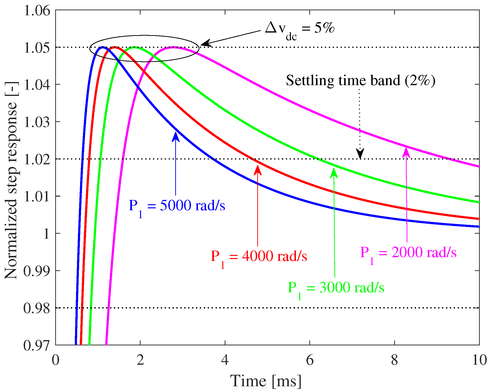
. To illustrate this condition, several values of
(and the associated values of
) were used to simulate the step response (
43) for a specific value of
m. The adopted value of
was obtained by solving Equation (
47) for a maximum overshoot
5%. Then, four values for
rad/s were tested, calculating the values of
rad/s using Equation (
42). The simulation results are presented in
Figure 8, where it is verified that the time response of
exhibits a maximum overshoot
5% for all the
conditions tested, which confirms the correctness of (
47). Moreover,
Figure 8 also shows that it is possible to design the settling time of
using the value of
; the procedure is presented in the next subsection.
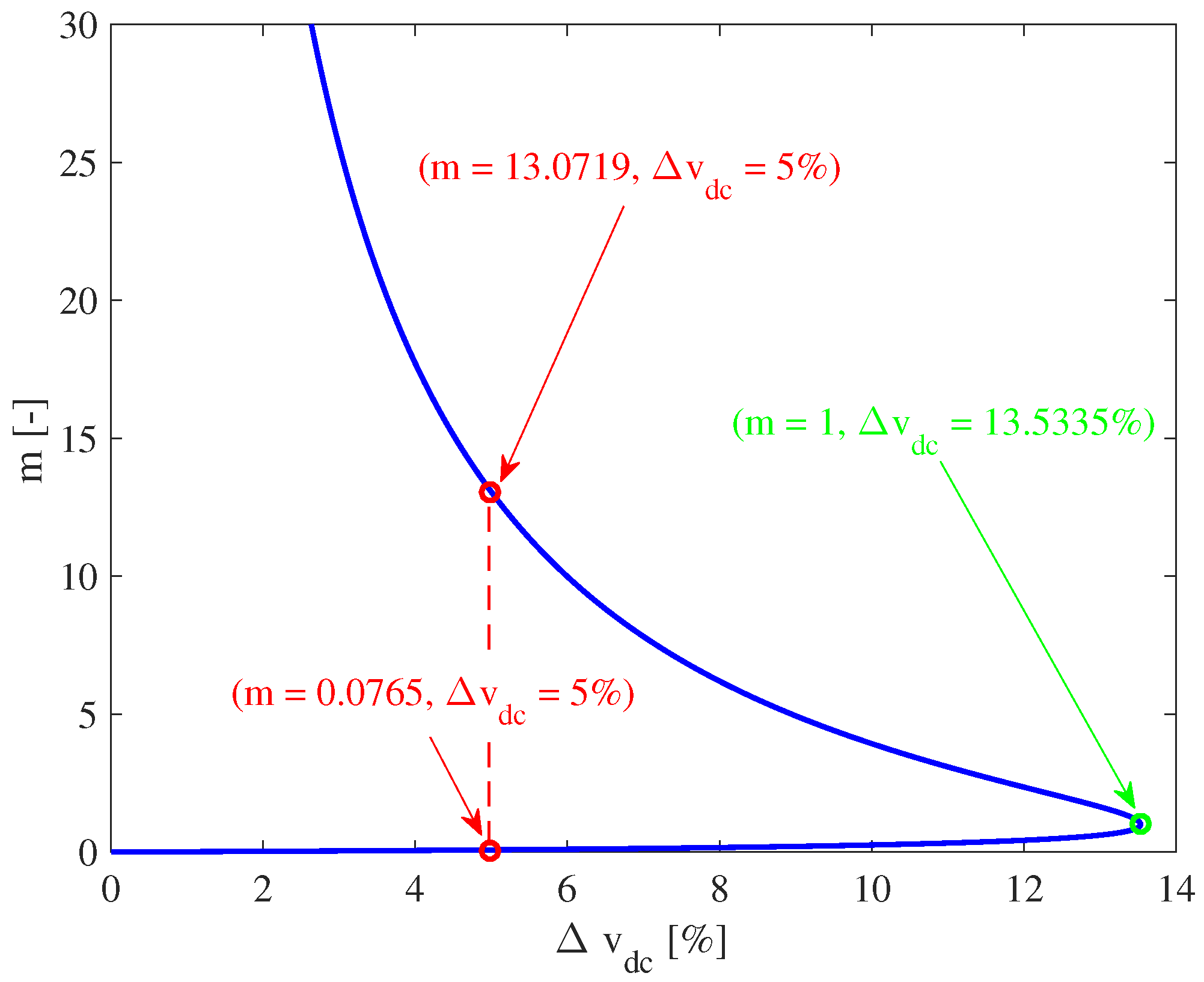
Expression (
47) has two limits. The first limit
0% occurs for
and
, which according to (
42) corresponds to
with a pole in infinity, i.e., a first-order transfer function. The second limit
13.5335% occurs for
, which according to (
42) corresponds to
with two real and equal poles. Therefore, the system response can be designed to have a maximum overshoot within
13.5335%. Moreover, Equation (
47) always has two equivalent solutions, as reported in
Figure 9, where
5% is obtained for
and
. For example, considering
rad/s and
results in
rad/s, while considering
rad/s and
results in
rad/s. Therefore, solving (
47) has two possible (and equivalent) domains for
m:
and
.
Figure 9 also indicates that
5% requires poles with a very large difference in magnitude, e.g.,
3% requires
, which could be difficult to implement.
4.3. Design of the Settling Time
The other performance criterion commonly used to specify the behavior of a DC bus corresponds to the settling of the voltage after perturbations. The value of is selected from the time that the load is able to operate in a condition different from the nominal voltage.
In this work,
is designed to provide a desired settling
measured at a given settling time band
, where the most classical band is
[
47].
Figure 8 shows that the settling time
occurs when the time response of the system (
43) is
. However, there are two crosses with
: one before the maximum overshoot and another one after the maximum overshoot. Therefore, the settling time fulfills
, where
corresponds to the time (
45) in which the maximum overshoot occurs.
On the basis of the previous analysis, the system response (
43) is rewritten as shown in (
48) to calculate the value of
that provides the desired settling time
for the band
, which includes the value of
m calculated in the previous section to impose the maximum overshoot. This equation must be solved using numerical methods, e.g., by using
fsolve from MATLAB.
To test the correctness of (
48), four instances of
were designed to guarantee a settling time of
ms for a band
considering different maximum overshoots.
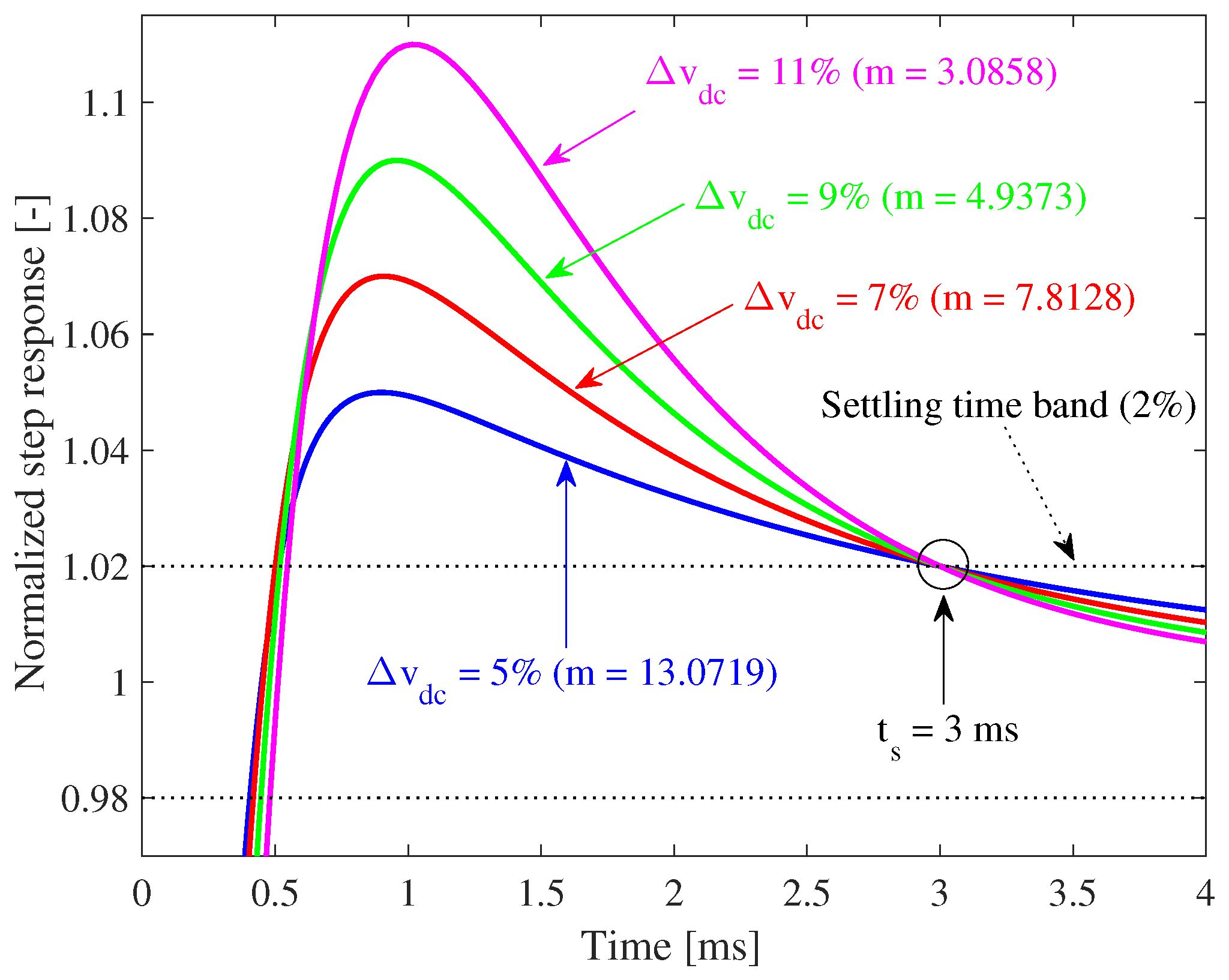
Figure 10 shows the simulation of these designs, which confirms that parameterizing the dynamic response using (
48) ensures that the desired settling time is fulfilled for any feasible value of
m.
Table 1 presents the maximum overshoots, the values of
m and the poles calculated using (
42), (
47) and (
48) depicted in
Figure 10.
4.4. Calculation of Parameters and
The sliding function (
3) and sliding surface are parameterized in terms of
and
. Therefore, the design of the sliding-mode dynamics in terms of the poles
and
must be translated to
and
values.
Contrasting the coefficients of
in both (
35) and (
39) leads to the following expressions for
and
:
These values of
and
must fulfill the constraints reported in (
16), (
20), (
21), (
24) and (
25) to ensure the global stability of the sliding-mode controller.
4.5. Summary
The design of the sliding-mode dynamics must be performed using the following steps:
6. Design Example and Simulation Results
This section presents a design example of the proposed controller for the charger/discharger circuit illustrated in
Figure 5. The DC/DC converter has the following passive elements:
H and
F. Moreover, the battery has a nominal voltage
V, and the DC bus voltage
must be regulated to
V. The controller design is performed by following the steps summarized in
Section 4.5.
This example considers a desired settling time
ms for a band
% and a maximum overshoot
%. Moreover, the parameter
is adapted continuously based on (
32), as reported in
Figure 12, dividing
by
. Then,
is calculated from (
47), and the pole
rad/s is calculated from (
48). The pole
rad/s is calculated by using (
42), and
A/V and
A/(V · s) are calculated using (
49) and (
50), respectively.
Considering a maximum supported battery current of
A and evaluating constraint (
16) results in
, which fulfills the transversality condition. Moreover, evaluating (
21) reveals that
fulfills the reachability conditions for
V; hence,
V. Similarly, evaluating (
25) indicates that such a
value fulfills the reachability conditions for
V; hence,
V. Therefore, the calculated values for
and
ensure global stability for the bus voltage
V.
The hysteresis band parameter
A was designed using (
60) to provide a steady-state switching frequency
kHz in stand-by mode (
A). This value of
H imposes steady-state switching frequencies equal to
kHz and
kHz for DC bus currents of
A (charge stage with
A) and 1 A (discharge stage with
A), respectively.
Figure 14 presents the circuit scheme implemented in the electrical simulator PSIM, in which the switching circuit and the synthesis of the sliding function are observed. This scheme uses a PI block and an adder from PSIM to implement the terms
of
; the transfer function of the PI block from PSIM is presented in (
63), where the PI block parameters
and
were calculated using the expressions presented in (
64).
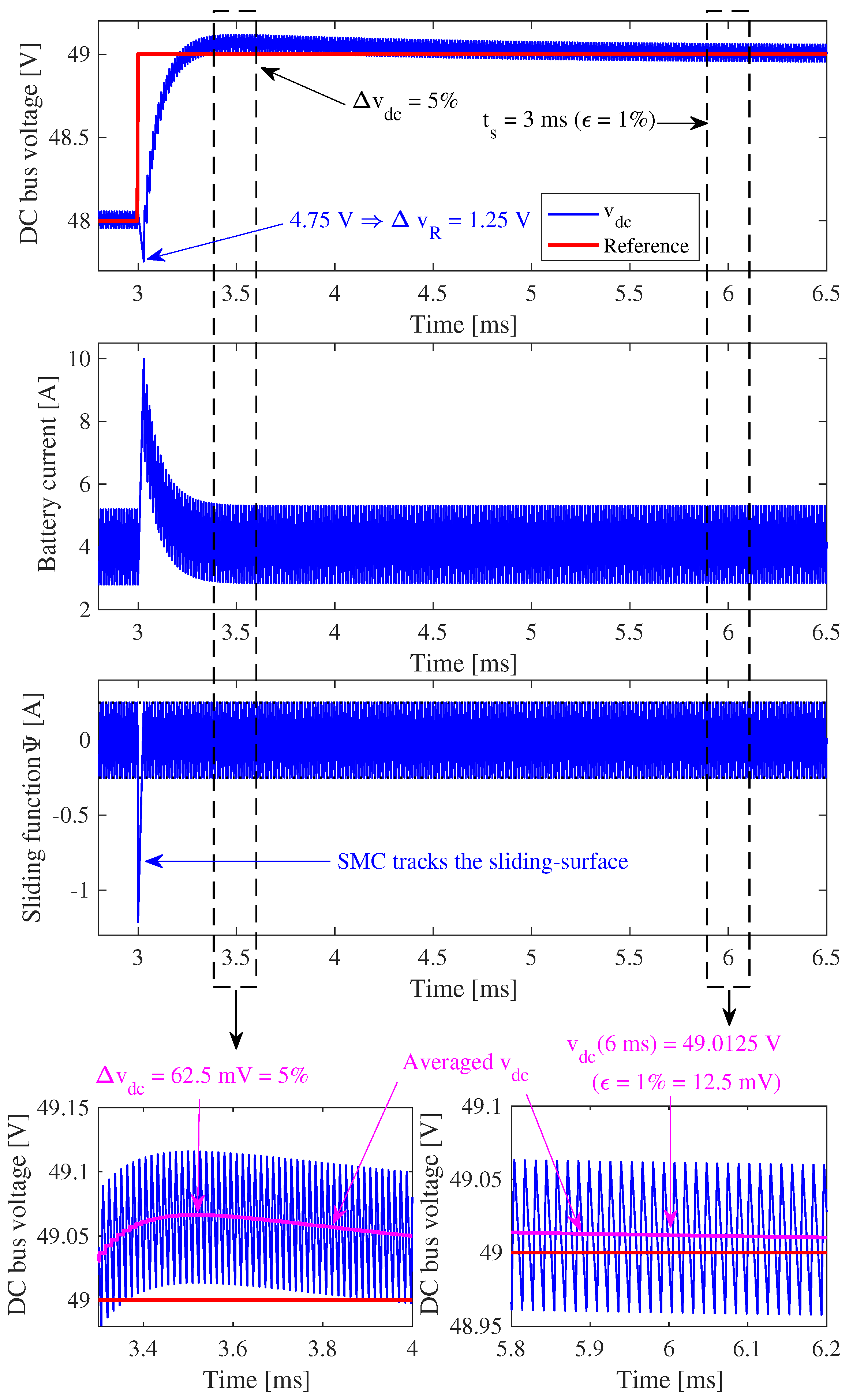
Figure 15 shows the simulation of the proposed sliding-mode controller with a step change of 1 V in the reference value. This simulation shows that the controller forces a fast change in the battery current to accelerate the bus voltage response. However, as described in
Section 5.3, this action requires
during the time in which the battery current is increased, forcing the bus capacitor to provide the bus current, which produces a small voltage drop
V. Therefore, the effective reference change faced by the controller is
V; this means that the maximum overshoot must be
V
mV, and the band
% corresponds to
V
mV. The magnified plots at the bottom of
Figure 15 confirm the correct behavior of the controller, where the maximum overshoot and settling time are measured with the average signal of
to remove the switching ripple.
The simulation also shows that the fast change in the reference value forces the sliding function to leave the surface during a very short time, but the fulfillment of the reachability conditions drives the system to return to the surface. This behavior demonstrates the global stability provided by the proposed solution. In conclusion, the controller performance presented in
Figure 15 verifies the correctness and accuracy of the analyses and design process proposed in the previous sections.
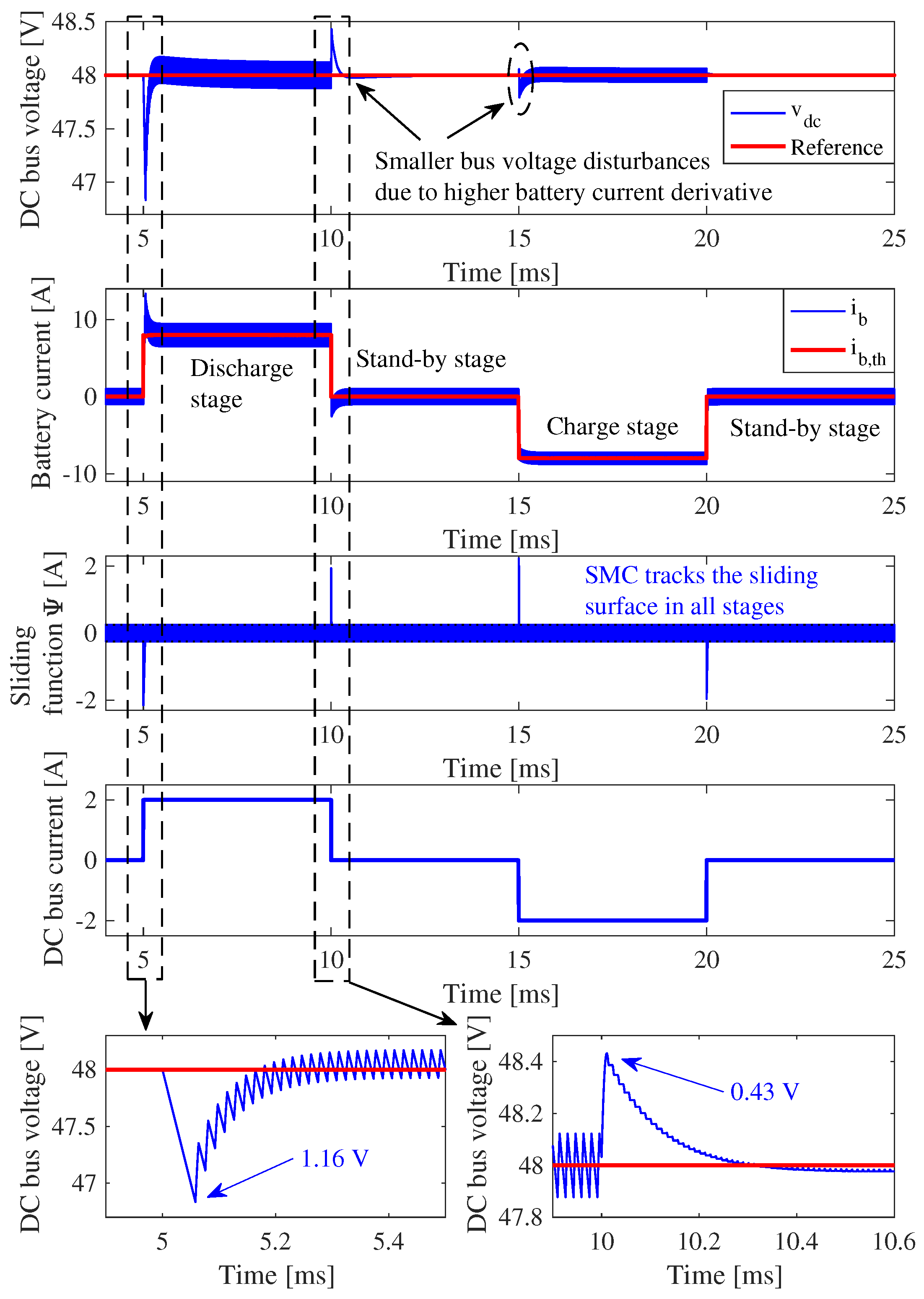
Figure 16 presents the simulation of the proposed SMC with perturbations in the DC bus current for all the operating conditions: stand-by stage (
A), charge stage (
A) and discharge stage (
A). The simulation considers step perturbations in the bus current with a magnitude equal to 2 A, which is 100% higher than the magnitude of the perturbations used to test the controller reported in [
15]. The simulation results demonstrate the satisfactory performance of the controller in compensating the bus current perturbations. Similarly, the simulation shows a fast and accurate tracking of the sliding surface in all the operating conditions. Note that the perturbations produce different deviations in the bus voltage: in the discharge stage, the battery current
increases with the slope
(
) and decreases with the slope
(
), which has a higher magnitude. Therefore, the transition from stand by to discharge is slower than the transition from discharge to stand by; hence, a larger voltage deviation occurs in the former transition. This comparison is presented in the magnified region at the bottom of
Figure 16.
In contrast, the transition from stand by to charge occurs with the slope (); hence, it produces a lower voltage deviation compared with the transition from stand by to discharge. Finally, the transition from charge to stand by occurs with the slope (), but due to the small voltage ripple in the stand-by condition, the voltage deviation is negligible.
Figure 17 presents an additional simulation that contrasts the performances of the proposed controller and the SMC without measuring
reported in [
15]. The results demonstrate the improved disturbance rejection provided by the proposed solution:
Bus current step from 0 A to 1 A (5 ms): the bus voltage deviation produced under the control of the new solution is only
of the deviation produced under the control of the solution in [
15].
Bus current step from 1 A to 0 A (10 ms): the bus voltage deviation produced under the control of the new solution is only
of the deviation produced under the control of the solution in [
15].
Bus current step from 0 A to
A (15 ms): the bus voltage deviation produced under the control of the new solution is only
of the deviation produced under the control of the solution in [
15].
Bus current step from
A to 2 A (20 ms): the bus voltage deviation produced under the control of the new solution is only
of the deviation produced under the control of the solution in [
15].
This improved disturbance rejection is due to the faster battery current response provided by the proposed SMC. Such a condition is observed in the magnified region at the bottom of
Figure 17, where the battery current imposed by the proposed SMC increases faster to compensate the bus current in a shorter time. This behavior results in a lower current extraction from the bus capacitor to provide a lower voltage deviation of the bus voltage.
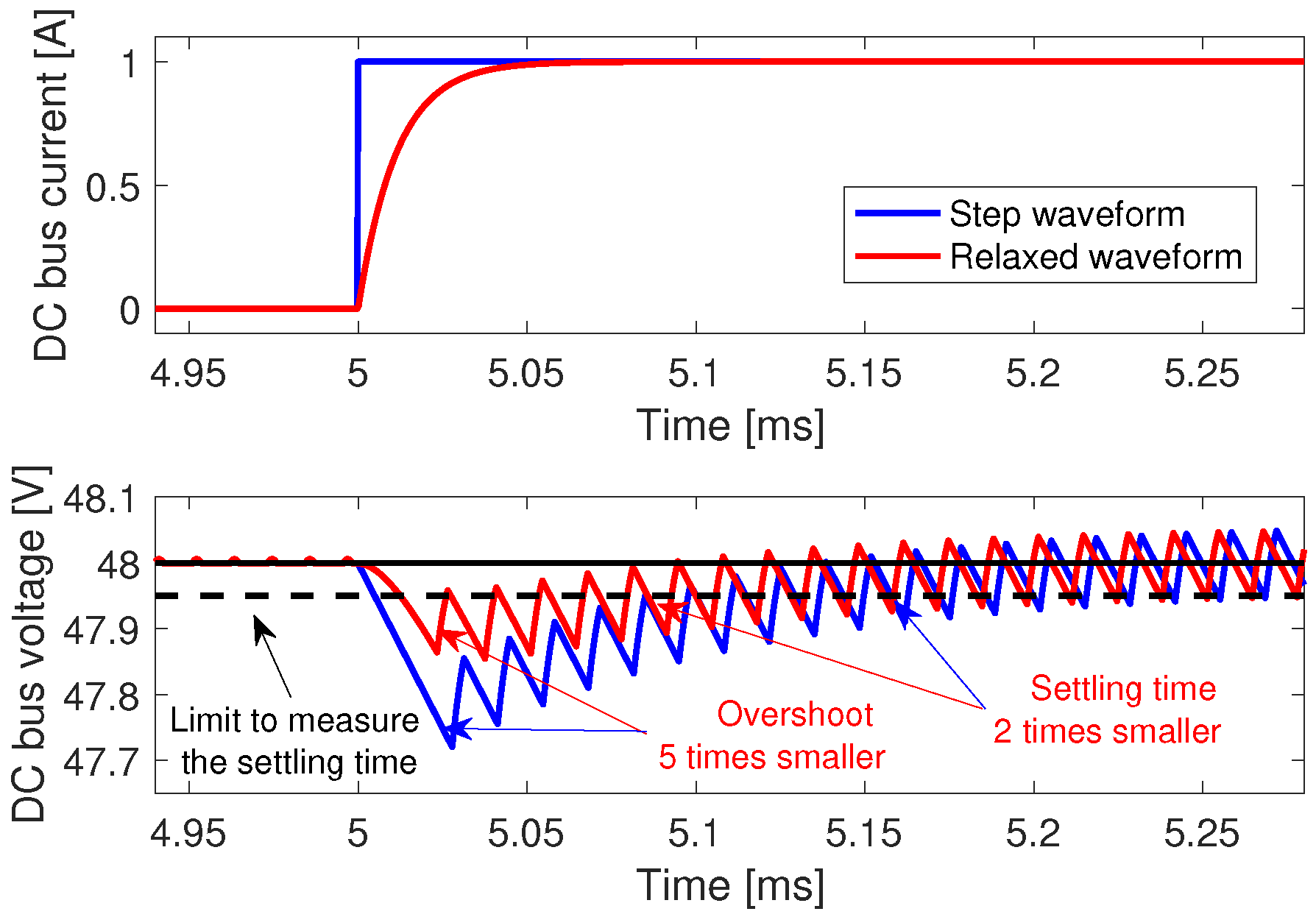
It must be noted that step-like current perturbations, similar to ones considered in the previous analyses and simulations, could be triggered by sudden connections and disconnections of loads and generators to/from the DC bus. However, some real loads require a charge produce, e.g., electrical machines, which produces a relaxed waveform with a limited frequency content. Therefore, since the control system developed in this paper considers the worst-case scenario (step-like perturbations), this solution will provide shorter settling times and overshoots in presence of relaxed waveforms.
Figure 18 shows the performance of the proposed SMC for both step-like and relaxed current perturbations in the DC bus: assuming a current transient with frequencies limited to 14 kHz (relaxed waveform), the maximum voltage overshoot is reduced 5 times and the settling time is reduced to the half, both in comparison with a step-like current transient (step waveform). Therefore, the solution proposed in this paper guarantees voltage overshoots and settling times smaller or equal to the limits defined in the design process.
7. Experimental Validation
To provide an experimental proof-of-concept, the battery charger/discharger and the proposed SMC were implemented as reported in
Figure 19. In particular,
Figure 19a shows the schematic diagram of the experimental platform. The prototype consists of a MT12330HR sealed lead-acid battery from MTEK [
50], a BOP 50-20GL four-quadrant source/load from Kepco [
51] to emulate the DC bus, the bidirectional power converter reported in
Figure 5, and digital and analog circuits implementing the sliding-mode controller.
The implementation of the sliding surface includes two current-sensing circuits based on the AD8210 [
52]: one of them measuring the DC bus current and the another measuring the battery current. Moreover, the DC bus voltage and battery voltage are scaled using voltage dividers. With this information, the adaptive surface of the SMC is calculated in a TMS320F28335 Delfino Microcontroller from Texas Instruments [
53].
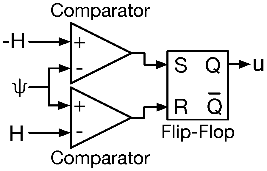
The hysteresis comparator was implemented with the timer TS555 [
49] according to
Figure 11, whose reference voltage is imposed by the TMS320F28335 through a MCP4822 digital-to-analog converter (DAC) [
54], and according to
Section 6, the hysteresis band was established as
A. However, this value was eventually scaled to a reference voltage within
V ± 0.83 V since the TS555 has a fixed
V. The TS555 output, i.e., the control signal
u, is delivered to the HIP4081A MOSFET driver [
55], which sets the states of both MOSFETs. The experimental setup is depicted in
Figure 19b.
With the aim of providing a comparative analysis between the solution proposed in this paper and the SMC reported in [
15], both SMCs were experimentally tested under the same conditions. Due to the physical limitations of the BOP 50-20GL four-quadrant source/load, the experiments consider relaxed current perturbations similar to the ones reported in
Figure 18. Moreover, some parameters of this experimental evaluation are different from the parameters used in the simulation examples presented in the previous section: the experimental DC/DC power converter has a 44
F capacitor and a 22
H inductor. Finally, the DC bus voltage is regulated at 36 V to have a safe margin from the maximum voltage supported by the BOP 50-20GL (50 V).
For the experimental tests, the dynamic response of the system was defined with a maximum overshoot of 5%, which requires, according to
Table 1, establishing the poles
and
at
rad/s and
rad/s, respectively, with
. Moreover, the settling time was set to 3 ms for
%. Then, using Equations (
49) and (
50), the parameters
A/V and
A/(V·s) were calculated. These values ensure the global stability of the system by fulfilling the transversality and reachability conditions reported in
Section 6.
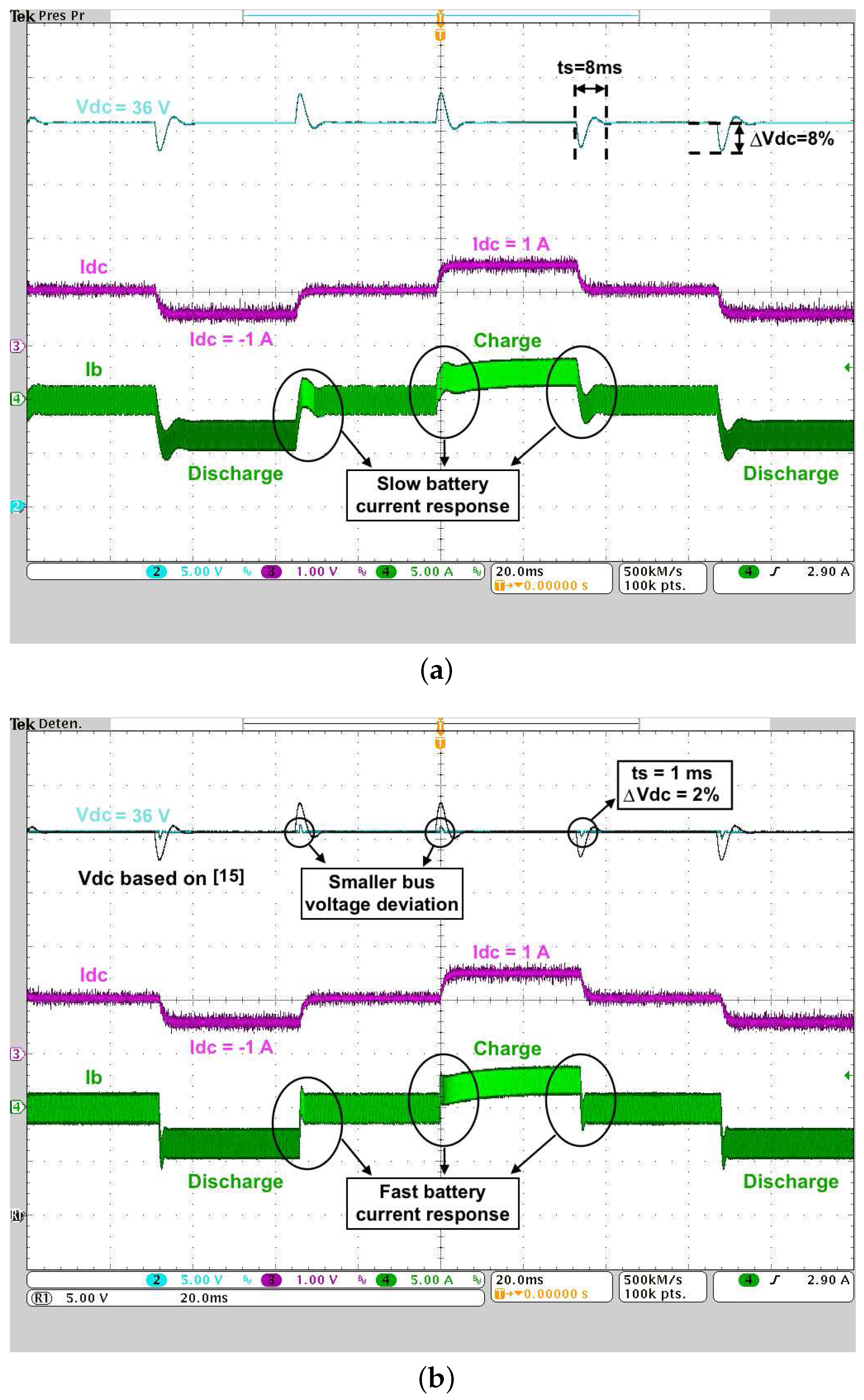
Figure 20a presents the waveforms obtained with the SMC reported in [
15]. The upper waveform shows the DC bus voltage, the middle one is the DC bus current, and the waveform at the bottom is the battery current. Similarly,
Figure 20b shows, in the waveforms at the top, the comparison of the DC bus voltages generated by both the proposed SMC and the SMC reported in [
15]. Moreover, the waveform in the middle is the same DC bus current, and the waveform at the bottom is the battery current generated by the proposed SMC.
To reproduce the simulations reported in
Figure 17, the experimental perturbations in the DC bus current have a magnitude of 1 A in the three operating conditions: charge, discharge and stand by.
Figure 20a shows the slow change in the battery current imposed by the SMC reported in [
15]; in contrast,
Figure 20b shows the fast change in the battery current imposed by the proposed SMC. This behavior enables the proposed SMC to provide a tighter voltage regulation. Moreover, the experiments consider a relaxed current waveform, hence the voltage overshoot and settling time must be smaller than the maximum limits imposed for the design process: 5% and 3 ms, respectively. In fact, the experimental voltage waveform reported in
Figure 20b exhibits an overshoot near to 2% and a settling time near to 1 ms. Finally, both
Figure 20a,b validate the analysis and simulations presented in the previous section and, simultaneously, demonstrate the correctness and implementation viability of the proposed solution.
8. Conclusions
This paper has presented a sliding-mode controller to regulate a bidirectional DC/DC converter interfacing a battery and a DC bus. The controller provides a satisfactory regulation of the DC bus voltage, improving the compensation of bus perturbations with respect to a previously reported solution. This tight bus regulation provides safe operating conditions to both the load and sources. The main feature of the new solution is the inclusion of the bus current in the sliding surface, which enables the controller to improve the compensation of bus perturbations. Moreover, the proposed design process ensures global stability in any operating condition, but at the price of the on-line calculation of one of the surface parameters, i.e., , which requires a fast microprocessor and ADC for the implementation.
The proposed SMC was tested under different operation conditions, achieving always the desired performance: the DC bus voltage exhibits limited voltage overshoots and settling times. In this way, the simulations reports a satisfactory match with the imposed criteria under the most extreme condition, i.e., step current perturbations. Moreover, the simulations also report smaller overshoots and settling times when the perturbations describe relaxed waveforms instead of ideal steps. Those results were confirmed by experimental measurements in a proof-of-concept platform, which ensures a safe operation of the DC bus under real conditions. Finally, both simulations and experiments were used to demonstrate the improved regulation with respect to a previously reported solution.
Another implementation challenge in power electronics is to avoid the current sensors, which are costly devices with high failure rates. For this topic, the mathematical analyses presented in this paper can be used to design an observer for the battery current. Moreover, replacing the classical boost (buck) charger/discharger with an interleaved structure will reduce the current ripple injected into the battery, which in turn will improve the battery health. These topics are currently under investigation.


