Article

Efficient Low-Cost IBC Solar Cells with a Front Floating Emitter: Structure Optimization and Passivation Layer Study

1
Wide Bandgap Semiconductor Technology Disciplines State Key Laboratory, School of Microelectronics, Xidian University, Xi’an 710071, China
2
SPIC Xi’an Solar Power Co., Ltd., Xi’an 710061, China
*
Authors to whom correspondence should be addressed.
Energies 2018, 11(4), 939; https://doi.org/10.3390/en11040939
Submission received: 23 March 2018 / Revised: 8 April 2018 / Accepted: 10 April 2018 / Published: 16 April 2018

Abstract

:
In this paper, we investigate interdigitated back contact solar cells with the front floating emitter structure systematically by using simulated and experimental methods. By comparing the front floating emitter structure with the front surface field structure, it is found that the efficiency of solar cells with the front surface field structure quickly reduces with the increasing of back surface field width; while solar cells with the front floating emitter structure can have a wider front surface field width range with minimum impact on the cell efficiency. More importantly, solar cells with the front floating emitter structure have a larger fabrication process tolerance, especially for the back surface field width, emitter width, and the bulk resistivity, which means that the fabrication process flow can be simplified and the production cost can be reduced. Based on the above results, large area (156.75 mm × 156.75 mm) interdigitated back contact solar cells with the front floating emitter structure are fabricated by using the simplified process with only one masking step. SiOx:B is used as the passivation layer, which can lead to a higher open circuit voltage and lower surface saturation current density. Finally, an efficiency of 20.39% is achieved for the large area solar cells.

1. Introduction

Interdigitated back contact (IBC) crystalline silicon solar cells are attracting much attention in the solar cells research society due to their potential to achieve a high power conversion efficiency by eliminating the shading losses altogether through putting both contacts on the rear of the cells [1,2]. Many institutes such as Fraunhofer ISE, ECN, and ISC-Konstanz are now working on IBC solar cells and their commercialization [3,4]. Some manufacturers such as SunPower and Trina have achieved over 24% efficiency on large area solar cells [5,6]. However, there are still many challenges for IBC solar cells, like a complex process flow and accurate alignment requirement compared with standard Al back surface field (Al-BSF) silicon solar cells, which increase the fabrication cost and become the bottleneck in mass production of IBC solar cells. To solve these problems, optimization of cell structure, simplification of process flow, and reduction of production cost have become the hot topics in IBC solar cells.
For conventional IBC solar cells, there is an n+-doped layer that forms the front surface field (FSF) on the front and the emitter to collect the minority carriers on the rear side separated by the non-collection area (BSF). The minority carriers generated in the region above BSF need to be transported laterally to the emitter region for collection. For a wide BSF width design, the travel distance of minority carriers generated in the region above BSF increases and the collection efficiency will be weak. Hermle et al. [7] called this effect an electrical shading effect. Due to the electric shading effect, the BSF width of FSF IBC solar cells should be less than 0.4 mm [8]. Narrow BSF width design means that a high accuracy pattern alignment is required, which will make the IBC solar cell process more complex and costly.
The front floating emitter (FFE) structure can be one optional solution to the electric shading effect. FFE structure with a p+ doped front surface floating junction instead of an n+ region on the front side can effectively reduce the composite loss caused by the minority carrier transversal transport process [9,10]. In FFE IBC solar cells, the holes generated in the region above BSF move to the nearest FFE, then laterally transport in the FFE, and finally reach the back emitter [8]. There is a lot of research work about the IBC solar cells with the FSF structure; however, the work about FFE IBC solar cells is relatively less abundant [7,11,12,13].
In this paper, we investigate FFE IBC solar cells systematically by using the simulated and experimental methods. By comparing the FFE structure with the FSF structure, it is found that FFE IBC solar cells can have a wider BSF width range with minimum impact on the cell efficiency. More importantly, FFE IBC solar cells have a larger structural parameter tolerance, especially for the BSF width, emitter width, and bulk resistivity, which means that the fabrication process flow could be simplified and the production cost is reduced. Based on the above results, we use a simplified process to fabricate large area (156.75 mm × 156.75 mm) FFE IBC cells with only one masking step. By using the SiOx:B as the passivation layer, an efficiency of 20.39% is achieved.

2. Simulation Results and Discussion

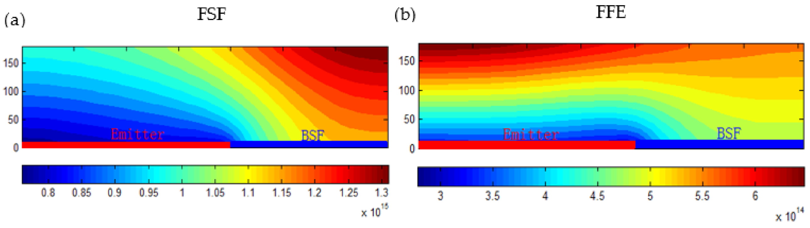
2.1. Carrier Transport Properties

We first investigate the minority carrier transport properties of both FSF and FFE IBC solar cells. Quokka 2D software was used for the simulation study. Figure 1 shows the cross-section of FFE IBC solar cells. The difference for the FSF IBC solar cells is that there is a front surface field instead of the floating emitter. Table 1 shows the parameters used in the simulation.
Figure 2a shows the calculated holes density gradient in the FSF structure. As is shown, the holes generated above the BSF have to move to the emitter region. The doped front surface produces a space charge region that drives the holes to move along the n-type silicon substrate toward the emitter. Usually, the transport path of the holes is much longer than the thickness of the silicon wafer, and recombination will inevitably occur during the transport process.
Figure 2b shows the calculated holes density gradient in the FFE structure. In the FFE structure, both the front surface floating junction and the back emitter can collect holes. The hole concentration of the front surface is higher than the back emitter hole concentration, so the transport process mainly depends on the FFE. The holes generated above the BSF region are collected by the front surface FFE first, and then propagate in the FFE to the region above the back emitter. Because there is a concentration gradient, the holes are re-injected to the back emitter, and collected by rear metal grids. This phenomenon, of holes passing through the FFE laterally and then being collected by the back emitter, is called the “pumping effect” [14]. Compared with the FSF structure, the recombination in the FFE structure will be smaller when the BSF width is large and then the carrier collection efficiency becomes larger, which will lead to a high solar cell efficiency.

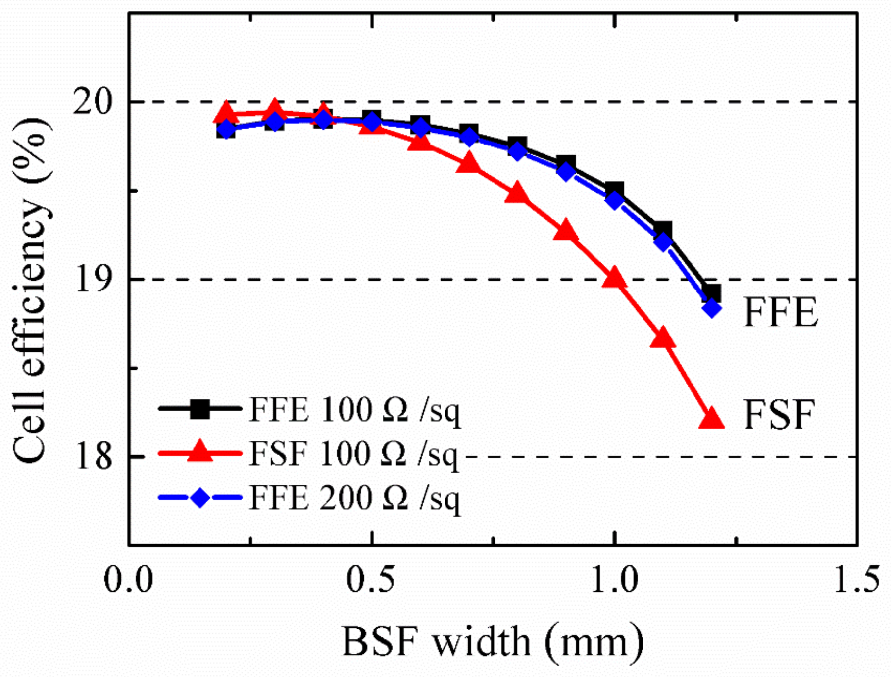
2.2. Effects of BSF Width on Solar Cell Efficiency

To investigate the effects of BSF width on the cell efficiency of both FSF and FFE IBC solar cells, the emitter width is fixed and the efficiency change with different BSF widths is shown in Figure 3. It can be seen that in both FSF and FFE structures, a narrower BSF produces a higher solar cell efficiency. Particularly, in the FSF structure, with the increase of the BSF width, the minority carrier transport path increases greatly, and the electrical shading loss leads to the rapid decrease of the solar cell efficiency, as shown in Figure 3. To avoid this effect, the typical BSF width for the FSF structure cell should be 0.2–0.4 mm. In the FFE structure, with the increase of BSF width, solar cell efficiency decreases at a much slower rate, i.e., the impact of BSF width is less in the FFE structure compared to the FSE structure. We also simulated FFE IBC solar cells with different front floating emitter sheet resistance. It can be seen from Figure 3, when increasing the sheet resistance from 100 Ω/sq to 200 Ω/sq, for 1 mm BSF width design, that cell efficiency only reduces by 0.05%. This indicates that the front surface emitter doping concentration can vary within a wide range with minimal impact on the solar cell conversion efficiency and thus the FFE structure has a wide process window, which is good, especially for mass production.

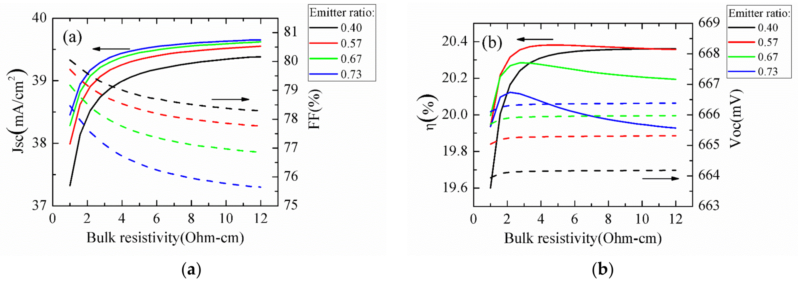
2.3. Influence of Different Resistivity and Emitter Width on FFE IBC Solar Cells

The emitter width ratio is an important factor which can affect the short-circuit current density and series resistance of IBC solar cells. When the BSF width is fixed, the increasing of the emitter width ratio means the increasing of the pitch width. Short-circuit current density Jsc [15] can be given by:
J s c = J s c , int Δ J o p t Δ J r e c
where J s c , int is the intrinsic short circuit current density, Δ J o p t is the short current density loss due to optical effects (reflection, transmission, and parasitic absorption etc.), and Δ J r e c is the short-circuit current density loss due to recombination. Δ J r e c can be further divided into Δ J r e c ,   e m i t t e r and Δ J r e c ,   s h a d , which are the recombination loss due to the emitter and recombination loss due to electrical shadow, respectively [16]. Δ J r e c ,   s h a d depends on pitch width, which can be given by:
Δ J r e c . shad ( P i t c h ) = α e l . shad P i t c h
where α e l . shad is the short-circuit current density loss due to recombination of the base, which is electrical shadow loss.
From Equations (1) and (2), J s c = J s c , int Δ J o p t Δ J r e c . emitter α e l . shad P i t c h , and Jsc increases with pitch width.
Series resistance of IBC solar cells can be given as:
R s ( V , P i t c h ) = R s , 0 ( V ) + R s , 1 ( V , P i t c h )
R s , 0 ( V ) includes the bulk resistance of vertical direction of the substrate, BSF resistance, contact resistance, and metal grids resistance [17]. R s , 1 ( V , P i t c h ) is the series resistance depending on the pitch width, including the emitter resistance and the lateral transmission resistance. R s , b a s e , l a t e r a l = 1 12 ρ b a s e d w a f e r × ( a n n ) 2 , where d w a f e r is the wafer thickness, a n n is the distance between the n+ and n+ doped regions, and ρ b a s e is the base resistivity. As the pitch width increases ( a n n increases), the cells’ lateral transmission resistance increases and the cells’ series resistance increases.
Figure 4 shows solar cell electrical parameters with different emitter width ratio and bulk resistivity values. In the simulation, the BSF area width is fixed at 600 μm, considering the alignment accuracy of the low-cost equipment like the screen printer. The pitch widths of the solar cell structure are 1000 µm, 1400 µm, 1800 µm, and 2200 µm with the corresponding emitter width ratio of 0.40, 0.57, 0.67, and 0.73, respectively. In Figure 4a, with the same resistivity, when the emitter width ratio increases, Jsc increases gradually because the increase in emitter width favours the collection of minority carriers. But when the emitter is wider, the transport path of the majority carriers generated in this region is also increased correspondingly, making the transport path larger than the thickness of the solar cell. From Equation (3), it results in an increase in the series resistance and causes a decrease in FF. In Figure 4b, the emitter size increases as the emitter width ratio increases, so that the back surface passivation effect is also increased, resulting in an increase in Voc. For the same emitter width ratio, since Voc is more dependent with the doping process, the simulation uses the same doping process, so as the resistivity increases, Voc remains unchanged. The simulation results show that for the emitter width ratio of 0.57 and corresponding pitch width of 1400 µm, the wafer resistivity can vary between 3 Ω·cm and 12 Ω·cm.

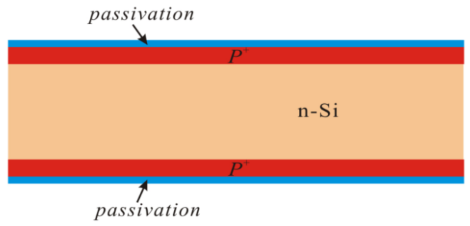
3. Experimental Results and Analysis

We used large area 156.75 mm × 156.75 mm Czochralski n-type monocrystalline silicon wafers for the experiments. The wafer thickness was 190 µm, and the wafer bulk lifetime was 2 ms. Two different resistivity wafers were used: 3 Ω·cm and 10 Ω·cm.
The process flow is shown in Figure 5. First, the wafers are saw damage etched and cleaned, and then the texturing was done by KOH solution to form random pyramids. POCl3 diffusion was used to form BSF on the rear side. After cleaning, the SiNx mask was deposited by using PECVD. Laser ablation was used to form the emitter area, and a single side etching step was used to remove the phosphorous diffusion at the laser ablation area. A tube diffusion furnace tube was used to form the FFE on the front surface of the silicon wafer, and also to form the emitter at the rear side. PECVD deposited SiNx layers were used as passivation and antireflective coating. Finally, screen printing metallization was used for IBC solar cells.
The experiment uses low-cost and simple production process, and the SiOx:B (boron-containing silicon oxide) is used as the passivation layer. In the process of boron diffusion, first, a layer of BSG was deposited on the surface of the silicon wafer at low temperature (870 °C–920 °C), then oxidized and driven-in at high temperature (950 °C–1000 °C) in oxygen atmosphere. 1% HF was used to remove a certain thickness of BSG layer, and the remaining SiOx:B layer was used as the passivation layer.

3.1. Influence of Thickness of SiOx:B Layer on Optical Properties

We conducted a simulation to study the influence of thickness of the SiOx:B layer on the optical properties. The incident light passes through the SiNx/SiOx:B structure to the doped silicon with a refractive index of 3.86. The refractive index of the upper SiNx antireflection layer is 2.05–2.12, and the refractive index of the lower SiOx:B passivation layer is 1.46. This structure causes the refractive index mismatch, which makes the SiNx/SiOx:B less reflective. The OPAL2 software was used to simulate the thickness matching of SiOx:B and SiNx layers. The reflectance, absorbance, and transmittance of different SiNx/SiOx:B structures are shown in Table 2.
From the simulation, the smaller the thickness of the SiOx:B layer, the better the transmittance of the SiNx/SiOx:B laminate structure. While the SiOx:B layer is thinner, the optimized SiNx thickness is closer to the optimized single SiNx layer, and the reflectivity of the reflected light at the SiNx and SiOx:B interfaces is lower.

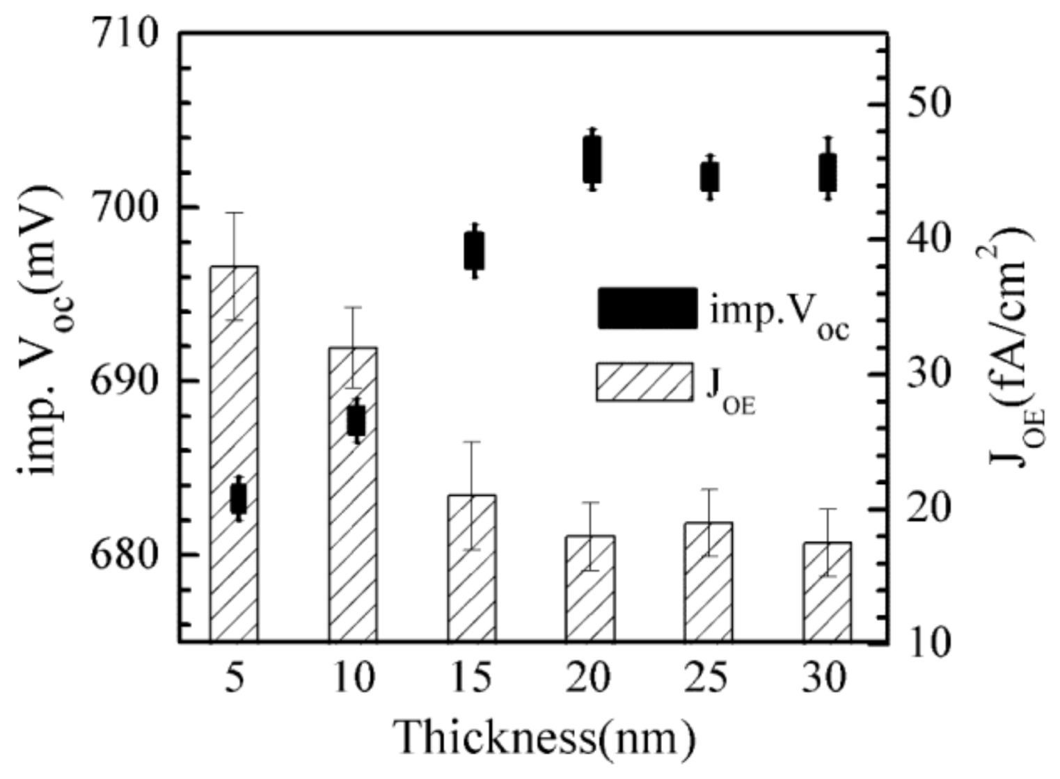
3.2. Effect of SiOx:B Layer Thickness on Passivation Quality

The p+/n/p+ symmetrical test structure is shown in Figure 6, which is used to test the passivation quality of different SiOx: B thicknesses. J0E and implied Voc were measured with the Sinton WCT-120 at a 1 × 1016 cm−3 injection level, as shown in Figure 7.
As shown in Figure 7, when the SiOx:B layer thickness is below 20 nm, implied Voc decreases with the decrease of SiOx:B layer thickness. When the SiOx:B layer thickness is 20 nm or above, J0E and implied Voc (reaches over 700 mV) remain unaffected with the different SiOx:B layer thicknesses, showing a good and stable passivation quality. This is because, when the SiOx:B is thin, its structure is not dense, and there are pinhole and induced defects. However, when the SiOx:B thickness is 20 nm or above, the SiOx:B layer becomes dense and it can effectively passivate the interface and prevent the effect of the external environment on the SiOx:B/Si interface.
On one hand, in order to achieve a better optical transmittance, the SiOx:B layer should be as thin as possible. On the other hand, in order to achieve a good passivation effect, the SiOx:B layer should be thicker than 20 nm. To balance the two sides, the optimum thickness of the SiOx:B layer is 20 nm.

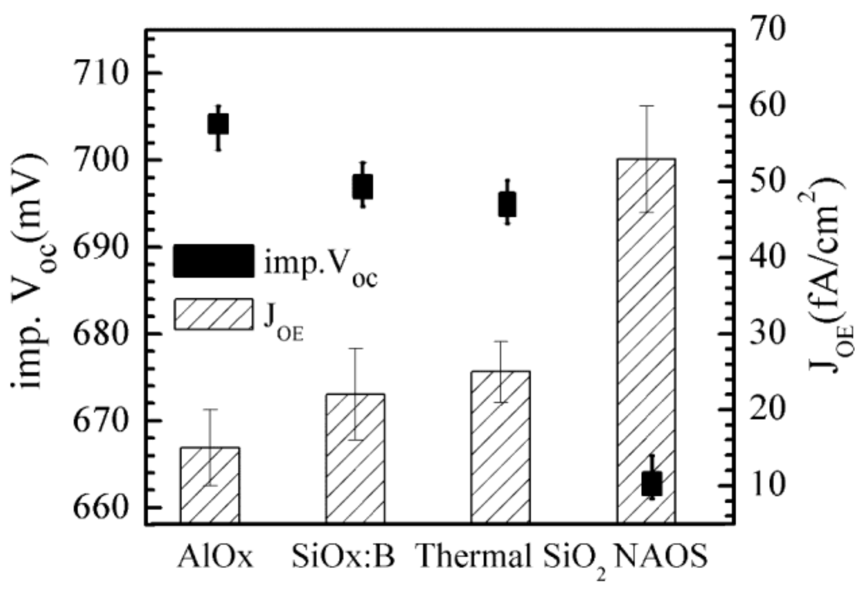
3.3. Comparison of Passivation Effect of Different Passivation Layers

Using the same symmetrical passivation structure shown in Figure 6, we compared four different passivation layers that are commonly used in industrial production. The silicon wafers are alkaline polished and boron diffused with a sheet resistance of 92 Ω/□ on both sides. Then, the samples were passivated by AlOx (PECVD), SiOx:B, thermal oxidation SiO2, and wet chemical SiO2 (NAOS), respectively. After passivation, the samples were capped on both sides with SiNx, and the passivation layer was activated with a firing furnace. J0E and implied Voc were measured with the Sinton WCT-120 at a 1 × 1016 cm−3 injection level, as shown in Figure 8.
The wet chemical grown SiO2 thickness is only 5 nm–10 nm, and the SiOx:B passivation quality is much better than NAOS. In addition, the SiOx:B passivation layer is grown at a high concentration of pure oxygen during the drive-in process of boron diffusion. On the other hand, the concentration of boron oxide in the BSG has been very low, which will greatly improve the melting point of BSG. The diffusion rate of SiO2 at the BSG/Si interface is higher than that of boron at the BSG/Si interface, so that the growth rate of SiO2 is larger than the boron diffusion rate in the BSG. Therefore, the impurity content of SiO2 at the silicon surface is very low, and the quality of the SiO2 layer can reach a similar level of thermal oxidation.
Since the SiOx:B passivation layer growth process can be integrated in the Boron diffusion process, the IBC solar cell process flow can be simplified and it can effectively reduce the production costs. In addition, previous study found that for IBC cell structure, the use of AlOx as emitter passivation will cause large efficiency degradation with reverse voltage, while the SiOx:B passivation layer did not find similar degradation [18]. Thus, the SiOx:B passivation layer is a good choice for the passivation.
Finally, solar cells were formed the base on the above simulation and passivation results using two different resistivity wafers. Table 3 shows the IV results of the cells. For high resistivity wafers, the impurity doped in the wafers is less and the solar cell short-circuit current density increases, while FF decreases with higher resistivity. The experiment results have a good match with the simulation results, as shown in Figure 4.

4. Conclusions

In this paper, we investigated the structure systematically for low cost FFE IBC solar cells. In the FFE structure, the front surface emitter has a pumping effect, which can increase the minority carrier lateral transport, and the electric shading effect is relatively small, which allows a wide BSF design. Simulation results show that for FSF IBC solar cells, the efficiency quickly reduced with the field width increasing; while FFE IBC solar cells can be designed with a wider back width and the efficiency loss is relatively smaller. The best cell efficiency was achieved with the emitter width ratio of 0.57. In addition, SiOx:B was used in FFE IBC solar cells, and its optical and passivation effects were investigated. High implied Voc and low J0E were achieved with SiOx:B passivation, which is similar to thermal oxidation passivation. It helps to reduce process steps and the production cost. Finally, large area (156.75 cm × 156.75 cm) IBC solar cells were fabricated with a simplified process flow and a cell efficiency of 20.39% was achieved.

Author Contributions

Y.Z. and C.Z. conceived the idea and guided the experiment; P.D. conducted most of the device simulation, fabrication, and data collection; H.G., C.Z., J.M., and X.Q. helped with the device measurement. All authors read and approved the manuscript.

Conflicts of Interest

The authors declare no conflicts of interest.

References

  1. Yang, G.; Ingenito, A.; Hameren, N.V.; Isabella, O.; Zeman, M. Design and application of ion-implanted polySi passivating contacts for interdigitated back contact c-Si solar cells. Appl. Phys. Lett. 2016, 108. [Google Scholar] [CrossRef]
  2. Procel, P.; Ingenito, A.; Rose, R.D.; Pierro, S.; Crupi, F.; Lanuzza, M.; Cocorullo, G.; Isabella, O.; Zeman, M. Opto-electrical modelling and optimization study of a novel IBC c-Si solar cell. Prog. Photovolt. Res. Appl. 2017, 25, 452–469. [Google Scholar] [CrossRef]
  3. Muller, R.; Schrof, J.; Reichel, C.; Benick, J.; Hermle, M. Back-junction back-contact n-type silicon solar cell with diffused boron emitter locally blocked by implanted phosphorus. Appl. Phys. Lett. 2014, 105. [Google Scholar] [CrossRef]
  4. Spinelli, P.; van de Loo, B.W.H.; Vlooswijk, A.H.G.; Kessels, W.M.M.; Cesar, I. Quantification of pn-junction recombination in interdigitated back-contact crystalline silicon solar cells. IEEE J. Photovolt. 2017, 7, 1176–1183. [Google Scholar] [CrossRef]
  5. Smith, D.D.; Cousins, P.J.; Masad, A.; Westerberg, S.; Defensor, M.; Ilaw, R.; Dennis, T.; Daquin, R.; Bergstrom, N.; Leygo, A.; et al. SunPower’s Maxeon Gen III solar cell: High Efficiency and Energy Yield. In Proceedings of the 39th IEEE PVSC, Tampa, FL, USA, 16–21 June 2013. [Google Scholar]
  6. Xu, G.C.; Yang, Y.; Zhang, X.L.; Chen, S.; Liu, W.; Chen, Y.; Li, Z.L.; Chen, Y.F.; Altermatt, P.P.; Verlinden, P.J.; et al. 6 inch IBC cells with efficiency of 23.5% fabricated with low-cost industrial technologies. In Proceedings of the 43rd IEEE PVSC, Portland, OR, USA, 5–10 June 2016. [Google Scholar]
  7. Hermle, M.; Granek, F.; Schultz, O.; Glunz, S.W. Shading Effects in Back-Junction Back-Contacted Silicon Solar Cells. In Proceedings of the 33rd IEEE PVSC, San Diego, CA, USA, 11–16 May 2008. [Google Scholar]
  8. Cesar, I.; Guillevin, N.; Burgers, A.R.; Mewe, A.A.; Koppes, M.; Anker, J.; Geerligs, L.J.; Weeber, A.W. Mercury: A back junction back contact front floating emitter cell with novel design for high efficiency and simplified processing. Energy Procedia 2014, 55, 633–642. [Google Scholar] [CrossRef]
  9. Granek, F.; Hermle, M.; Huljic, D.M.; Schultz, O.; Glunz, S.W. Enhanced lateral current transport via the front N+ diffused layer of n-type high-efficiency back-junction back-contact silicon solar cells. Prog. Photovolt. Res. Appl. 2009, 17, 47–56. [Google Scholar] [CrossRef]
  10. Burgers, A.R.; Guillevin, N.; Mewe, A.A.; Suvvi, A.; Spinelli, P.; Weeber, A.W.; Cesar, I. FFE IBC cells: Impact of busbars on cell performance with circuit modelling. Energy Procedia 2015, 77, 21–28. [Google Scholar] [CrossRef]
  11. Magnone, P.; Debucquoy, M.; Giaffreda, D.; Posthuma, N.; Fiegna, C. Understanding the influence of busbars in large-area IBC solar cells by distributed spice simulations. IEEE J. Photovolt. 2015, 5, 552–558. [Google Scholar] [CrossRef]
  12. Yang, G.T.; Zhang, Y.; Procel, P.; Weeber, A.; Isabella, O.; Zeman, M. Poly-Si(O)x passivating contacts for high-efficiency c-Si IBC solar cells. Energy Procedia 2017, 124, 392–399. [Google Scholar] [CrossRef]
  13. Müller, R.; Reichel, C.; Schrof, J.; Padilla, M.; Selinger, M.; Geisemeyer, I.; Benick, J.; Hermle, M. Analysis of n-type IBC solar cells with diffused boron emitter locally blocked by implanted phosphorus. Sol. Energy Mater. Sol. Cells 2015, 142, 54–59. [Google Scholar] [CrossRef]
  14. Burgers, A.R.; Cesar, I.; Guillevin, N.; Mewe, A.A.; Spinelli, P.; Weeber, A.W. Designing IBC cells with FFE: long range effects with circuit simulation. In Proceedings of the 43rd IEEE PVSC, Portland, OR, USA, 5–10 June 2016. [Google Scholar]
  15. Kluska, S.; Granek, F.; Rudiger, M.; Hermle, M.; Glunz, S.W. Modeling and optimization study of industrial n-type high-efficiency back-contact back-junction silicon solar cells. Sol. Energy Mater. Sol. Cells 2010, 94, 568–577. [Google Scholar] [CrossRef]
  16. Hermle, M.; Granek, F.; Schultz, O.; Glunz, S.W. Analyzing the effects of front-surface fields on back-junction silicon solar cells using the charge-collection probability and the reciprocity theorem. J. Appl. Phys. 2008, 103. [Google Scholar] [CrossRef]
  17. Mohr, A. Silicon concentrator cells in a two-stage photovoltaic system with a concentration factor of 300x. In Fakultat fur Angewandte Wissenschaften; University Freiburg: Freiburg, Germany, 2005. [Google Scholar]
  18. Muller, R.; Reichel, C.; Yang, X.; Richter, A.; Benick, J.; Hermle, M. Long term stability of solar modules made from compensated Sog-Si or Umg-Si solar cells. Energy Procedia 2017, 124, 365–370. [Google Scholar]
Figure 1. Cross-section of FFE IBC solar cells. The dashed box indicates the unit cells used in the device simulations.
Energies 11 00939 g001
Figure 2. Gradient of the holes density in the simulated IBC cell structures: (a) FSF and (b) FFE.
Energies 11 00939 g002
Figure 3. Efficiency of FFE IBC and FSF IBC cells with different BSF widths. Also shows the cell efficiency for different FFE sheet resistance values.
Energies 11 00939 g003
Figure 4. Solar cell electrical parameters with different emitter width ratio and bulk resistivity values. (a) Change in Jsc and FF with different emitter width ratio and bulk resistivity values; (b) Change in Efficiency and Voc with different emitter width ratio and bulk resistivity values.
Energies 11 00939 g004
Figure 5. Flow chart of the cells fabrication process steps.
Energies 11 00939 g005
Figure 6. Symmetric structure for passivation quality test.
Energies 11 00939 g006
Figure 7. J0E and implied Voc change with SiOx:B thickness.
Energies 11 00939 g007
Figure 8. Comparison of J0E and implied Voc with different passivation layers.
Energies 11 00939 g008
Table 1. Parameters used in this simulation work.
Parameter NameValue
cell thickness190
emitter diffusion half width400
base diffusion half width300
emitter contacts width60
base contact width60
n-type bulk resistivity10 Ω·cm
bulk lifetime2 ms
emitter diffusion sheet resistance90 Ω/□
base diffusion sheet resistance70 Ω/□
FSF sheet resistance100 Ω/□
FFE sheet resistance100/200 Ω/□
emitter diffusion J0-passivated40 fA/cm2
emitter diffusion J0-contacted80 fA/cm2
base diffusion J0-passivated50 fA/cm2
base diffusion J0-contacted100 fA/cm2
front diffusion J030 fA/cm2
emitter contact resistance<1 × 10⁻⁶ Ω·cm2
base contact resistance1 × 10−4 Ω·cm2
external series resistance0.38 Ω·cm2
effective intrinsic carrier density ni, eff9.65 × 109 cm-3
Table 2. Effect of different SiOx:B layer thicknesses on the optical properties.
SiOx:B Thickness (nm)SiNx Thickness (nm)Reflectance (%)Absorption (%)Transmittance (%)
5744.10.595.4
10714.30.595.2
15674.60.594.9
206450.594.5
25605.30.594.2
30575.80.593.7
Table 3. IV results of FFE IBC cells.
Resistivity (Ω·cm)Voc (mV)Jsc (mA/cm2)FF (%)η (%)
3663.139.0278.520.31
10662.939.5477.820.39

