Article

An Enhanced Hybrid Switching-Frequency Modulation Strategy for Fuel Cell Vehicle Three-Level DC-DC Converters with Quasi-Z Source

1
School of Electrical and Information Engineering, Tianjin University, 92 Weijin Rd, Nankai District, Tianjin 300072, China
2
Changchun Power Supply Company, 4799 Renmin Street, Changchun 130022, China
3
Department of Electrical and Electronic Engineering, University of Nottingham Ningbo China, Ningbo 315100, China
4
Department of Electrical and Electronic Engineering, University of Nottingham, Nottingham NG7 2RD, UK
*
Author to whom correspondence should be addressed.
Energies 2018, 11(5), 1026; https://doi.org/10.3390/en11051026
Submission received: 28 March 2018 / Revised: 18 April 2018 / Accepted: 19 April 2018 / Published: 24 April 2018
(This article belongs to the Collection Electric and Hybrid Vehicles Collection)

Abstract

:
For fuel cell vehicles, the fuel cell stack has a soft output characteristic whereby the output voltage drops quickly with the increasing output current. In order to interface the dynamic low voltage of the fuel cell stack with the required constant high voltage (400 V) of the inverter DC link bus for fuel cell vehicles, an enhanced hybrid switching-frequency modulation strategy that can improve the voltage-gain range is proposed in this paper for the boost three-level DC-DC converter with a quasi-Z source (BTL-qZ) employed in fuel-cell vehicles. The proposed modulation strategy retains the same advantages of the original modulation strategy with more suitable duty cycles [1/3, 2/3) which avoids extreme duty cycles. Finally, the experimental results validate the feasibility of the proposed modulation strategy and the correctness of its operating principles. Therefore, the BTL-qZ converter is beneficial to interface the fuel cell stack and the DC bus for fuel cell vehicles by using the proposed modulation strategy.

1. Introduction

With the increase of the number of automobiles, more and more attention has been paid to the environmental pollution caused by automobile exhaust emissions. Almost all governments are increasing the research and development of renewable energy vehicles, including plug-in hybrid electric vehicles, blade electric vehicles with hybrid energy sources, and fuel cell vehicles [1,2,3].
Fuel cells are electrochemical devices that process hydrogen and oxygen to generate electric power, leaving water vapour as their only by-product. Fuel cell vehicles are an important contributor to those clean energy vehicles and have been applied widely in practice, due to the advantages of the environmental friendship, the reliability and the high efficiency [4,5,6,7]. However, the fuel cell has a “soft” output characteristic—its output voltage drops quickly with an increase of the output current [8,9,10,11,12,13]. Therefore, the fuel cell stack has to be interfaced with the inverter high voltage (400 V) DC link bus through a step-up DC-DC converter with a wide voltage-gain range [14,15].
Regarding the previously described characteristic of the fuel cell, many wide input-voltage range boost converters have been presented. Cascaded boost DC-DC converters were proposed in [16,17]. The interleaving structure was applied in the front-end of the converter for reducing the input current ripple [18], and interfacing the input side with the high voltage side (i.e., the DC link bus) by the second boost stage. Even though a high voltage-gain with a wide input-voltage range can be realized by such a structure, many disadvantages, such as a reduced efficiency, increased volume, a complex controller and low reliability still exist. In order to simplify the converter structure between the fuel cell stack and the DC link bus, and improve the operating performance of fuel cells [19,20], a non-isolated DC-DC converter with a coupled inductor was proposed in [21], where a high voltage-gain can be achieved by only one power stage. However, it suffers from the high voltage stress across the power semiconductors, due to the leakage inductance, which reduces the efficiency and the reliability of this converter [22]. Although the voltage stress can be reduced by an active-clamped circuit in [23], the active-clamped switch added and the floating gate driver increase both the circuit complexity and the cost. In addition, some optimized DC-DC converters are proposed for PV generation systems and the auxiliary power supply of fuel cell vehicles [24,25], with the synchronous rectification and zero voltage switching (ZVS) operations. As to the power interface between the fuel cells and the DC bus for fuel cell vehicles, a wide voltage-gain range is required.
Z source net has been applied in the traditional step-up DC-DC converters to achieve the higher voltage-gain [26], but this converter may introduce additional maintenance and safety issues for fuel-cell vehicles, due to the penalty of the discontinuous input current and the non-common grounds between the input and the load sides. To solve this issue, a quasi-Z source circuit was presented in [27,28,29]. It can be used in the step-up DC-DC converters with the merits of the lower capacitor voltages and the common ground [30]. For the better application of the step-up DC-DC converters with the quasi-Z source, a combination of the improved common ground three-level converter was applied in [31,32,33] and the quasi-Z network was proposed in [34], namely a wide input-voltage range Boost three-level DC-DC converter with a quasi-Z source (BTL-qZ) for fuel cell vehicles, as shown in Figure 1.
This topology was controlled by the phase-shifted 180-degree modulation strategy as shown in Figure 2 [34]. The equivalent frequency of the inductor current in the BTL-qZ converter is twice the switching frequency, as shown in Figure 2l,m, which reduces the output current ripple of the fuel cell source. In addition, the voltage of the flying-capacitor can be clamped well at half of the output voltage by the total capacitor voltages of the quasi-Z source net, and the voltage stress across all power semiconductors is half of the output voltage. The step-up voltage-gain M1 of the BTL-qZ DC-DC converter can be obtained as:
M 1 = 2 3 4 m
where m is the modulation index for Q1 and Q2 in Figure 1, and 0.5 ≤ m < 0.75.
Because there are only three switching states (S1S2 = 01, S1S2 = 10, and S1S2 = 11, where “0” represents the turn-off of power switches Q1, Q2) existing for the BTL-qZ converter, when it is controlled by the phase-shift 180-degree modulation strategy, namely S1S2 = 00 is absent in [34]. In this paper, an enhanced hybrid switching-frequency modulation strategy without any extra hardware is proposed to further improve the voltage-gain range for the BTL-qZ DC-DC converter. Because it contains the switching state S1S2 = 00 in each switching period for the BTL-qZ converter. As a result, its voltage-gain range can be improved significantly, comparing with the phase-shifted 180-degree modulation strategy.
This paper is organized as follows: in Section 2, the operating principles of the converter controlled by the hybrid switching-frequency modulation strategy are analysed in detail, and the voltage-gain is deduced. The comparisons between the proposed modulation strategy and the original phase-shifted 180-degree modulation strategy from the aspects of voltage-gain and the stresses on the components are shown in Section 3. The application of the converter for fuel cell vehicles is presented in Section 4. In Section 5, the experimental results measured from the prototype controlled by the hybrid switching-frequency modulation strategy are shown and analysed finally, a summary of the proposed modulation strategy for the BTL-qZ converter is presented and the conclusion is delivered in Section 6.

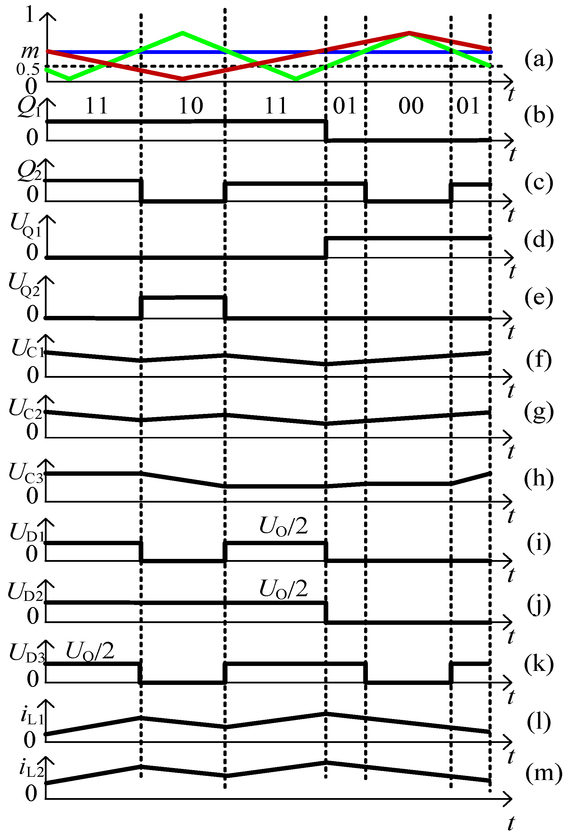
2. Operating Principle of the Hybrid Switching-Frequency Modulation Strategy

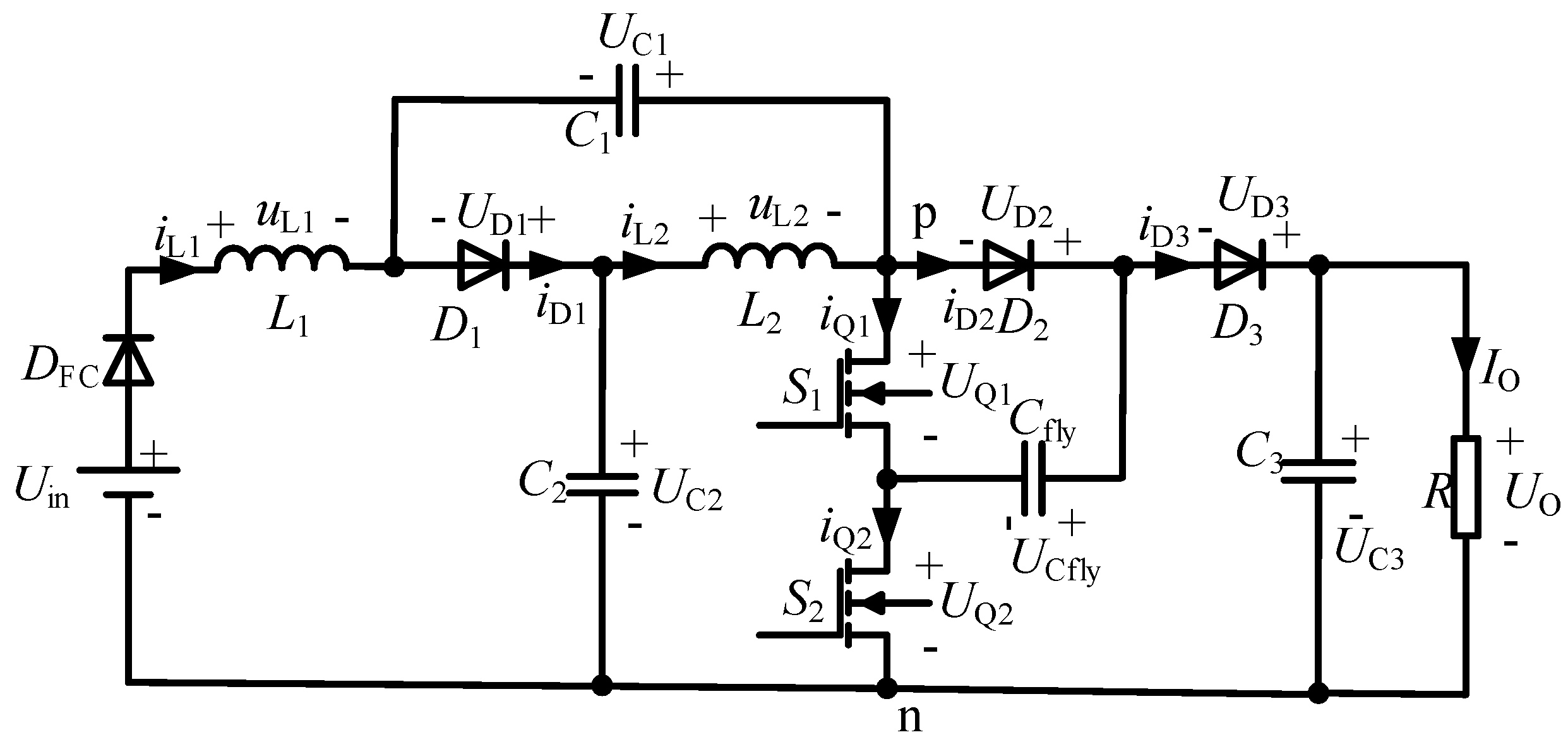
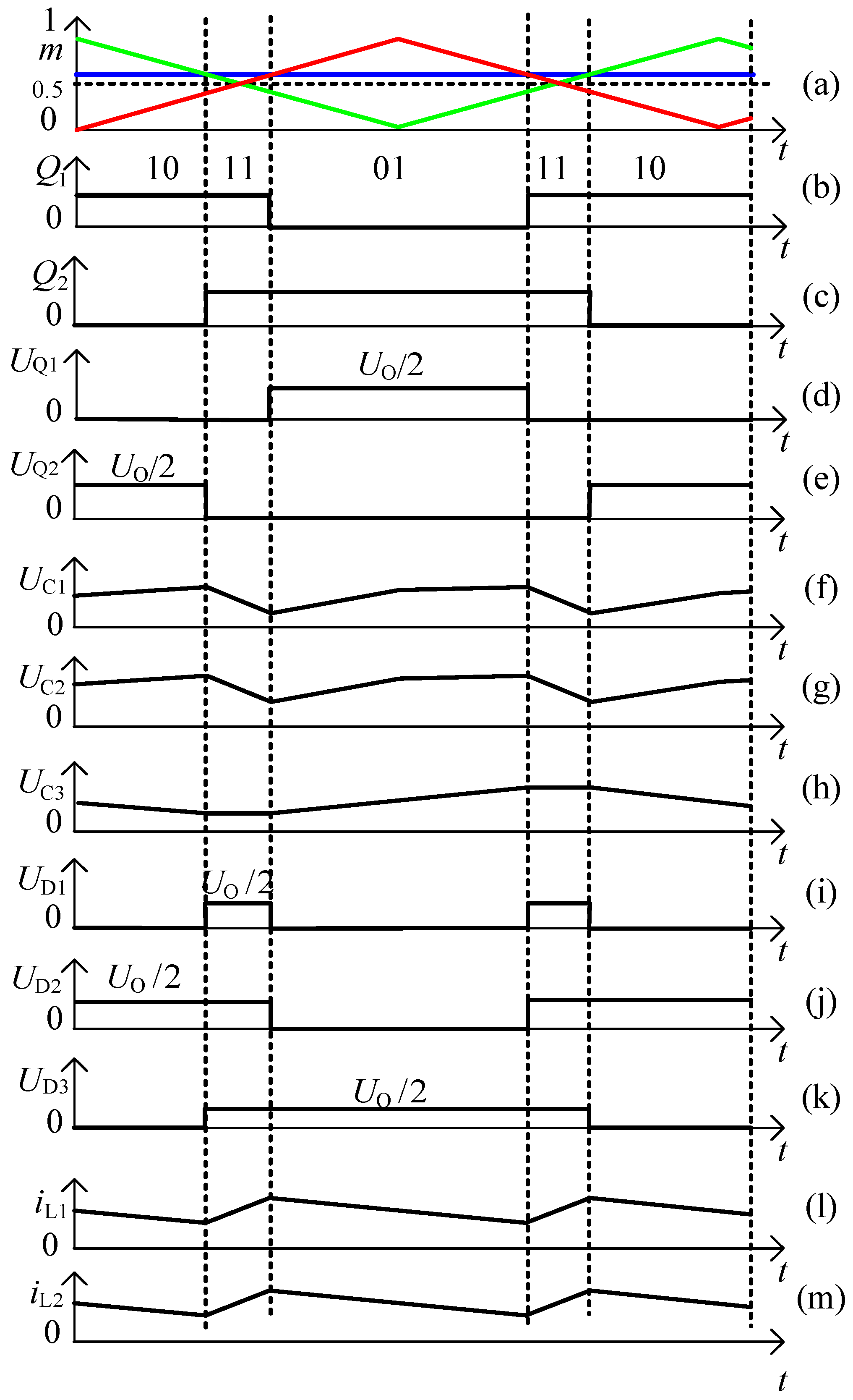
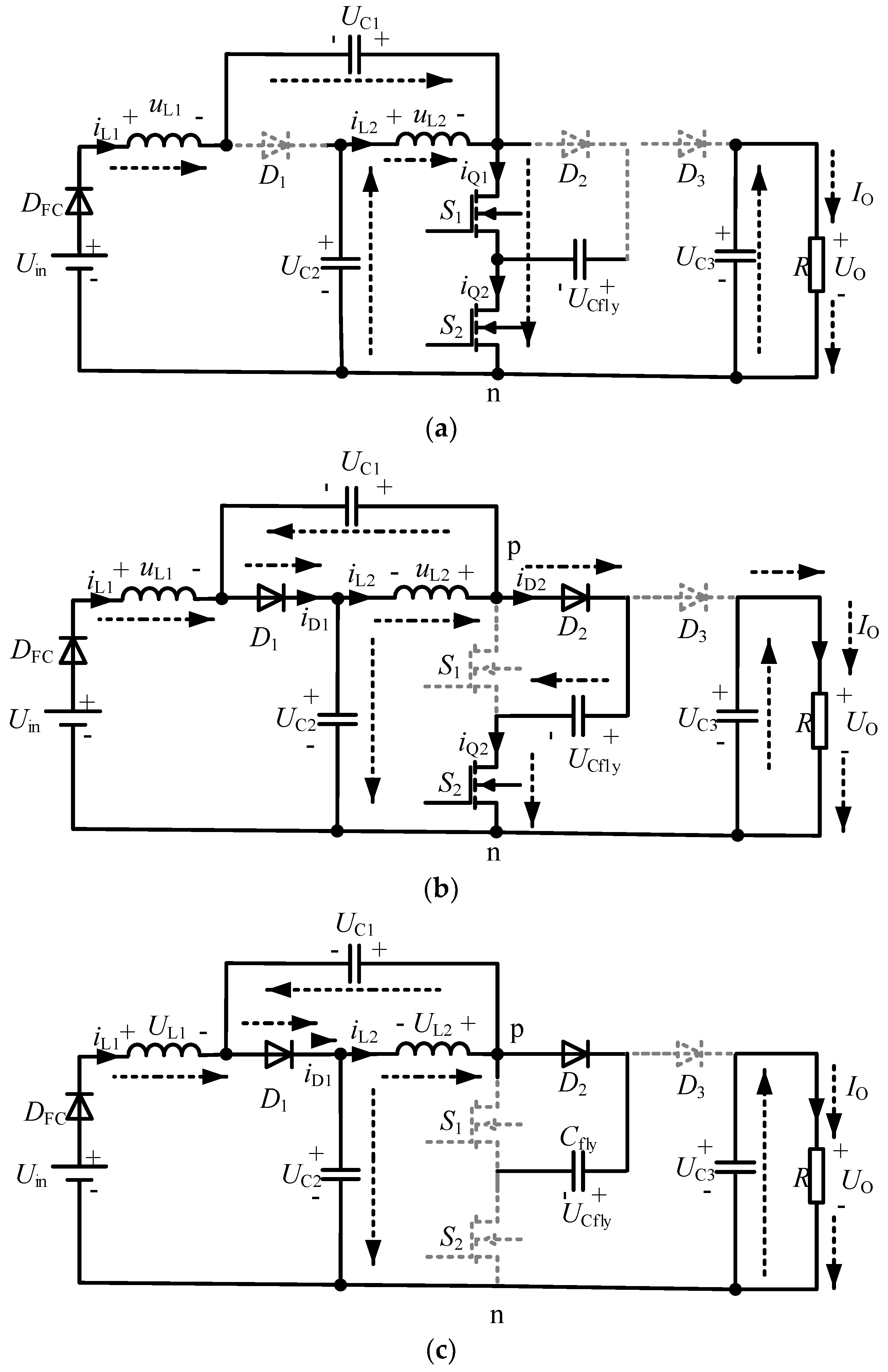
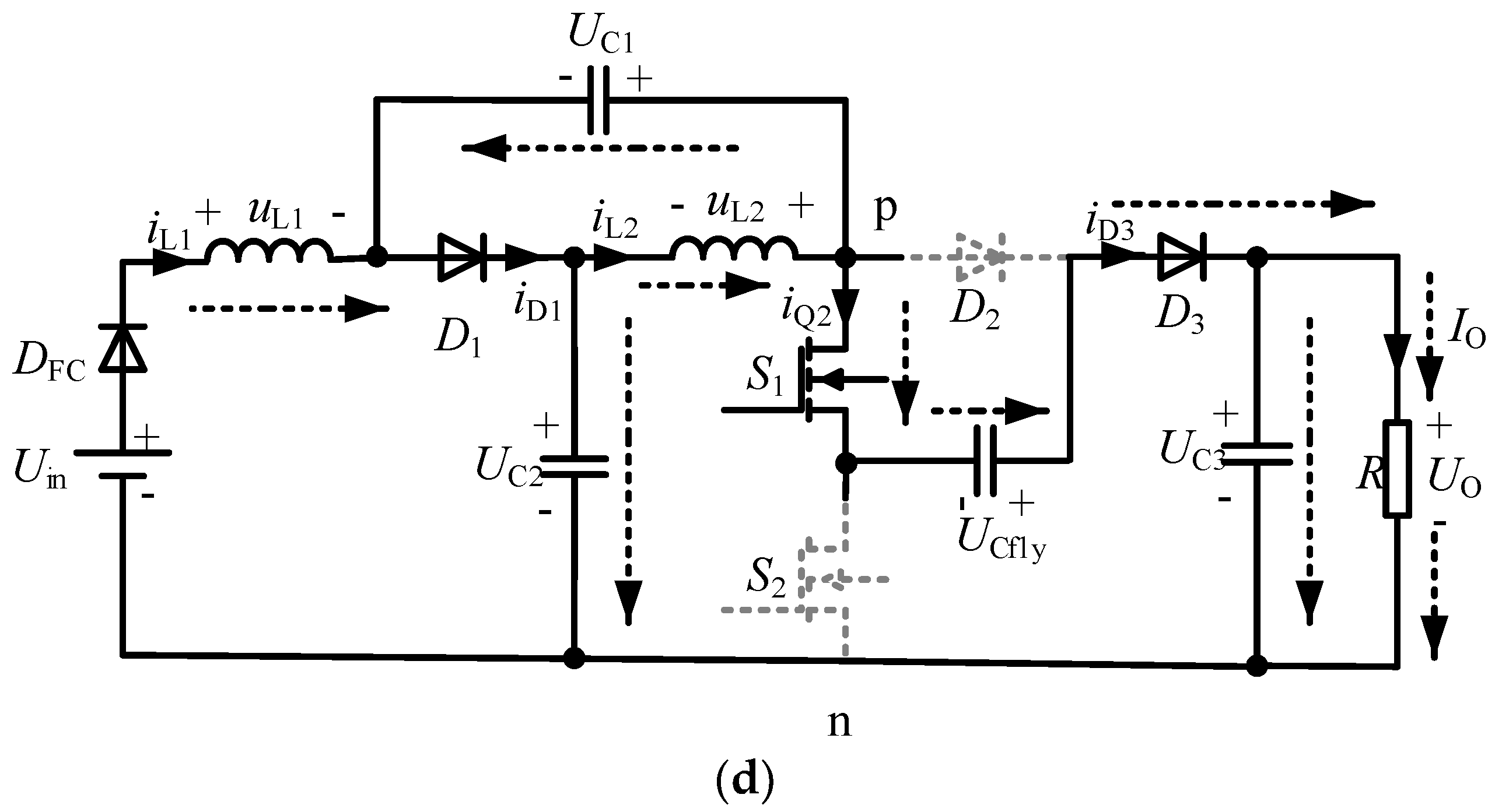
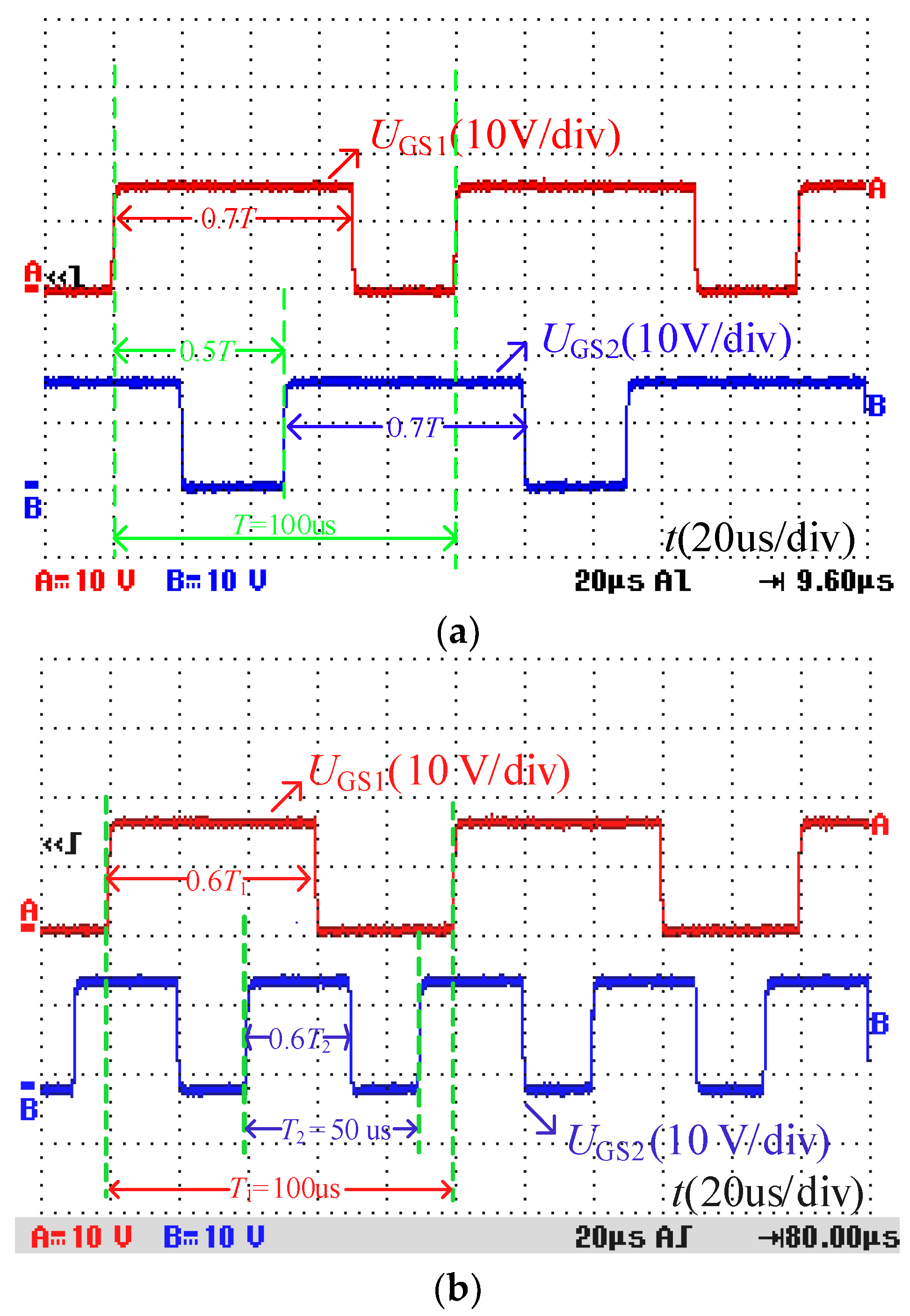
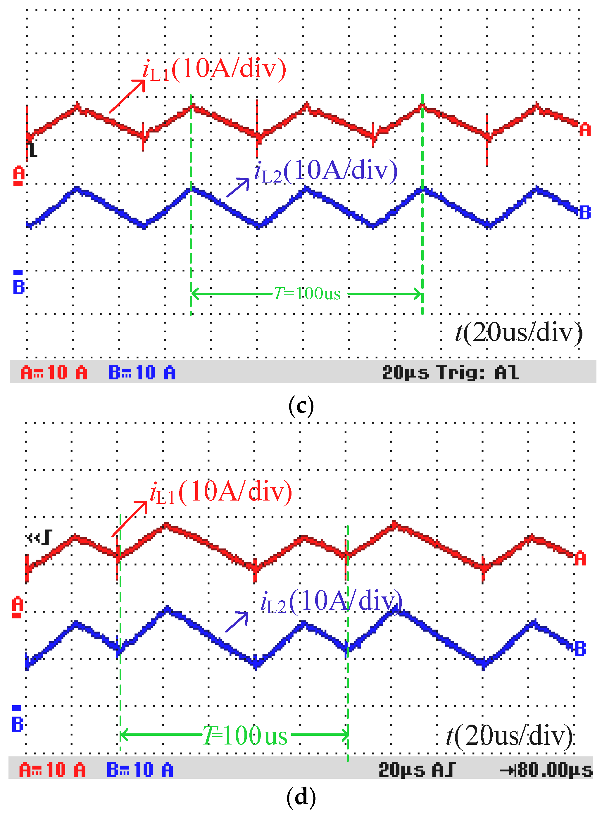
2.1. Analysis of Operating States
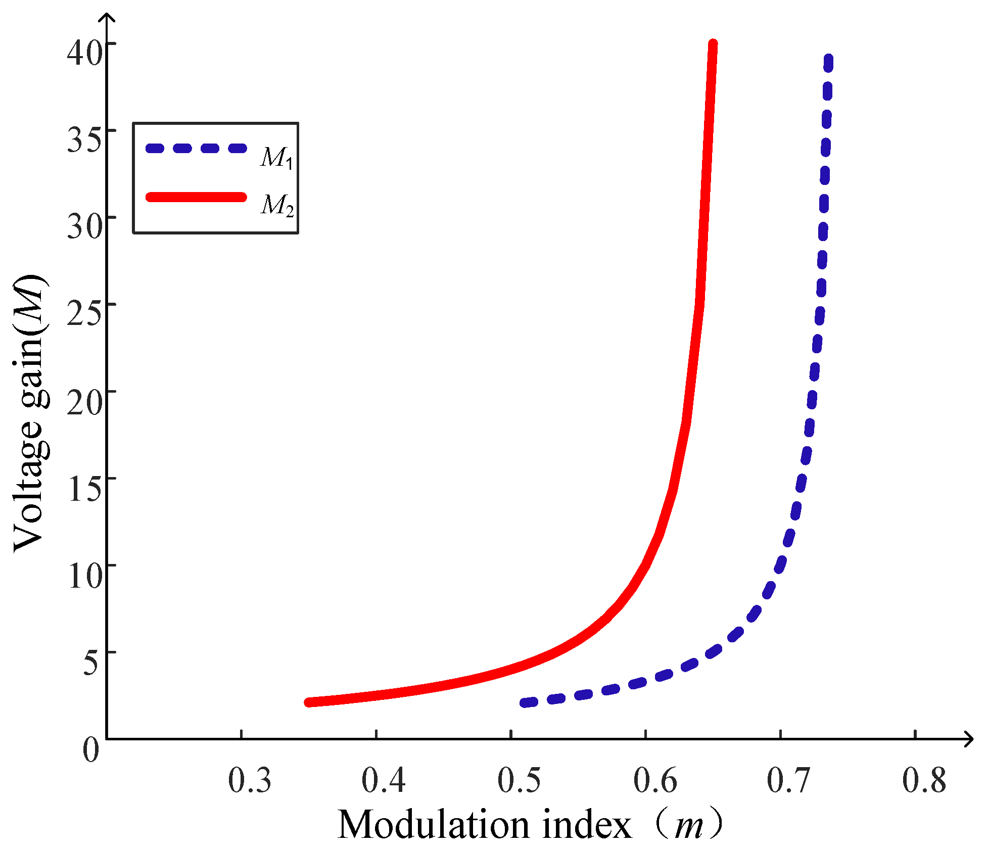
There are two power switches in the topology as shown in Figure 1, and the corresponding gate signals can be modulated in theory by two carriers and two modulation waves. Therefore, there are four combination modes for two carriers: with the same frequency and the different phases, with the same frequency and the phase, with the different frequencies and the same phase, and with the different frequencies and phases. In addition, the modulation indices can also be different. Therefore, the modulation methods for the BTL-qZ converter are flexible and various in theory. The phase-shifted 180-degree modulation strategy in [34] is implemented by the two gate signals with the same duty cycles and the 180-degree phase difference. Under the control of the phase-shifted 180-degree modulation strategy, the switching state S1S2 = 00 (as shown in Figure 3c) is absent. In order to improve the operating performance by containing the switching state S1S2 = 00, the hybrid switching-frequency modulation strategy is proposed in this paper. The carrier frequency of Q2 is twice the carrier frequency of Q1. In addition, the gate signals of Q1 and Q2 have the same modulation index.
Figure 4 shows the key waveforms of the BTL-qZ converter controlled by the hybrid switching-frequency modulation strategy. According to Figure 4b,c, there are six switching processes in each switching period of Q1, i.e., “S1S2 = 11→10→11→01→00→01”. Therefore, the inductors can charge and discharge twice in each switching period of Q1 respectively. The currents of L1 and L2 are shown in Figure 4l,m. The energy flow paths of the BTL-qZ converter in different switching states are shown in Figure 3. The analysis of the different switching states are summarized as follows:
(1) S1S2 = 11: According to the equivalent circuit of this switching state in Figure 3a, and the key waveforms in Figure 4, Q1 and Q2 are both turned on, while diodes D1D3 are all turned off. Therefore, the input voltage source Uin and the capacitor C1 transfer the energy to the inductor L1 through the diode DFC and the power switches Q1 and Q2. C2 transfers the energy to L2 through Q1 and Q2. Due to the conduction of Q1 and Q2, and the turn-off of D2 and D3, the cathode of Cfly is connected to the ground, and the anode of Cfly is suspended. So the voltage across Cfly keeps invariant. Capacitor C3 supplies the energy for the load.
(2) S1S2 = 01: There are four energy flow loops in this switching state as shown in Figure 3b. L2 is discharging, at the same time C1 is charging through D1. The inductor current iL2 and the capacitor voltage UC1 are shown in Figure 4m,f. L1 and Uin connected in series are discharging, while C2 is charging through DFC and D1. Thus the inductor current iL1 and the capacitor voltage UC2 can be illustrated in Figure 4l,g. L1, L2 and Uin in series are discharging, while the flying-capacitor Cfly is charging through DFC, D1, D2, and Q2. Capacitor C3 supplies the energy for the load.
(3) S1S2 = 00: From the equivalent circuit in Figure 3c, and the key waveforms in Figure 4, diodes D1 and D2 are turned on, while Q1 and Q2 are both turned off. Hence, Uin and L1 transfer the energy to C2 through the diode DFC and D1, L2 transfers energy to C1 through D1, and capacitor C3 supplies the energy for the load. In addition, due to the turn-off of Q1 and Q2, the anode of Cfly is suspended. So the voltage across Cfly keeps invariant, which is similar to the switching state S1S2 = 11.
(4) S1S2 = 10: D2 is turned off due to the reverse voltage across Cfly, and Q2 is turned off. At the same time, D1, D3 and Q1 are turned on. As a result, there are three energy flow paths left, as shown in Figure 3d. Cfly, Uin, L1, and L2 connected in series are discharging to supply the energy for the load and C3 through DFC, D1, Q1 and D3. Uin and L1 transfer energy to C2 through DFC and D1. L2 transfers energy to C2 through D1.
When S1S2 = 01, as shown in Figure 3b, Q2 is turned on, namely UQ2 = 0. By means of Kirchhoff’s Voltage Laws (KVL), UCfly can be obtained as follows:
U Cfly = U C 1 + U C 2
Based on Figure 3c and KVL, when the switching state changes from “S1S2 = 01” to “S1S2 = 00”, UCfly can be described as follows:
U Q 2 = U C 1 + U C 2 U Cfly
According to (2) and (3), when S1S2 = 00, the voltage stress across Q2 is also equal to zero, namely UQ2 = 0. Therefore, when the switching state changes from “S1S2 = 01” to “S1S2 = 00”, Q2 can be turned off in the zero voltage switching. When the switching state changes from “S1S2 = 00” to “S1S2 = 01”, Q2 can be turned on in the zero voltage switching. According to the gate signal and the corresponding voltage stress across Q2 in Figure 4c,e, the frequency of the voltage across Q2 is half the frequency of the gate signal of Q2. Therefore, the switching losses of power switches can be reduced due to this special characteristic of hybrid switching-frequency modulation strategy.

2.2. Voltage-Gain

In order to simplify the analysis, the operating conditions are assumed as follows:
(1)
The capacitance of the capacitors in Figure 1 is infinite, as well as the inductance of the inductors. Therefore, capacitors are regarded as constant voltage sources, and inductors can be considered as constant current sources.
(2)
All the power semiconductors and energy storage components are in the ideal conditions, namely the on-state resistances of the power semiconductors, the forward voltage drops of the diodes, and the equivalent series resistances (ESRs) of the inductors and capacitors are ignored.
According to Figure 3a–d, there are four switching states in a switching period of Q1. The durations of the corresponding states can be expressed as t1, t2, t3 and t4 respectively. The carrier frequencies for the gate signals of Q1 and Q2 are f and 2f respectively, and the modulation index (m) for Q1 and Q2 is equal. The durations of the four switching states in a switching period of Q1 can be obtained as follows by means of Figure 4a–c:
{ t 1 = ( 3 m 1 ) / f t 2 = ( 1 m ) / f t 3 = ( 1 m ) / f t 4 = ( 1 m ) / f
In addition, the BTL-qZ converter operates within the range 1/3 < m < 1 to guarantee the existence of the switching state sequence “11→10→11→01→00→01”.
When the BTL-qZ converter operates in the continuous conduction mode, the voltage-second balance equations can be obtained as follows:
{ U C 2 U in × t 2 + t 3 + t 4 = U in + U C 1 × t 1 U C 1 × t 2 + t 3 + t 4 = U C 2 × t 1
The capacitor voltages across C1, C2 and Cfly can also be obtained by Equations (4) and(5):
{ U C 1 = 3 m 1 4 6 m U in U C 2 = 3 3 m 4 6 m U in U Cfly = U C 1 + U C 2 U Cfly = U O 2
As a result, the step-up voltage-gain M2 of the BTL-qZ converter controlled by the proposed modulation strategy can be obtained by means of (4)–(6) as follows:
M 2 = 2 2 3 m
where 1/3 < m < 2/3.

3. Comparisons between Proposed and Original Modulation Strategies

3.1. Comparisons of Voltage Gain

In Figure 5, the comparison of voltage gain M versus modulation index m between the proposed and the original modulation strategies is obtained by means of (1) and (7). According to Figure 5, the relationship between the voltage gains is M2 > M1, when m > 0.5 and the modulation indices for the proposed and the original modulation strategies are both equal. Therefore, compared with the original modulation strategy in [34], the BTL-qZ converter controlled by the proposed modulation strategy benefits from the higher voltage-gain. In addition, the maximum effective modulation index for the proposed modulation strategy is less than 2/3, which is much closer to 0.5 than that for the original modulation strategy which is “0.75”. Hence, when the same high voltage-gain is required, comparing with the original modulation strategy in [34], the modulation index of the proposed modulation strategy is closer to 0.5, namely the proposed modulation strategy benefits from avoiding the extreme duty cycle better.

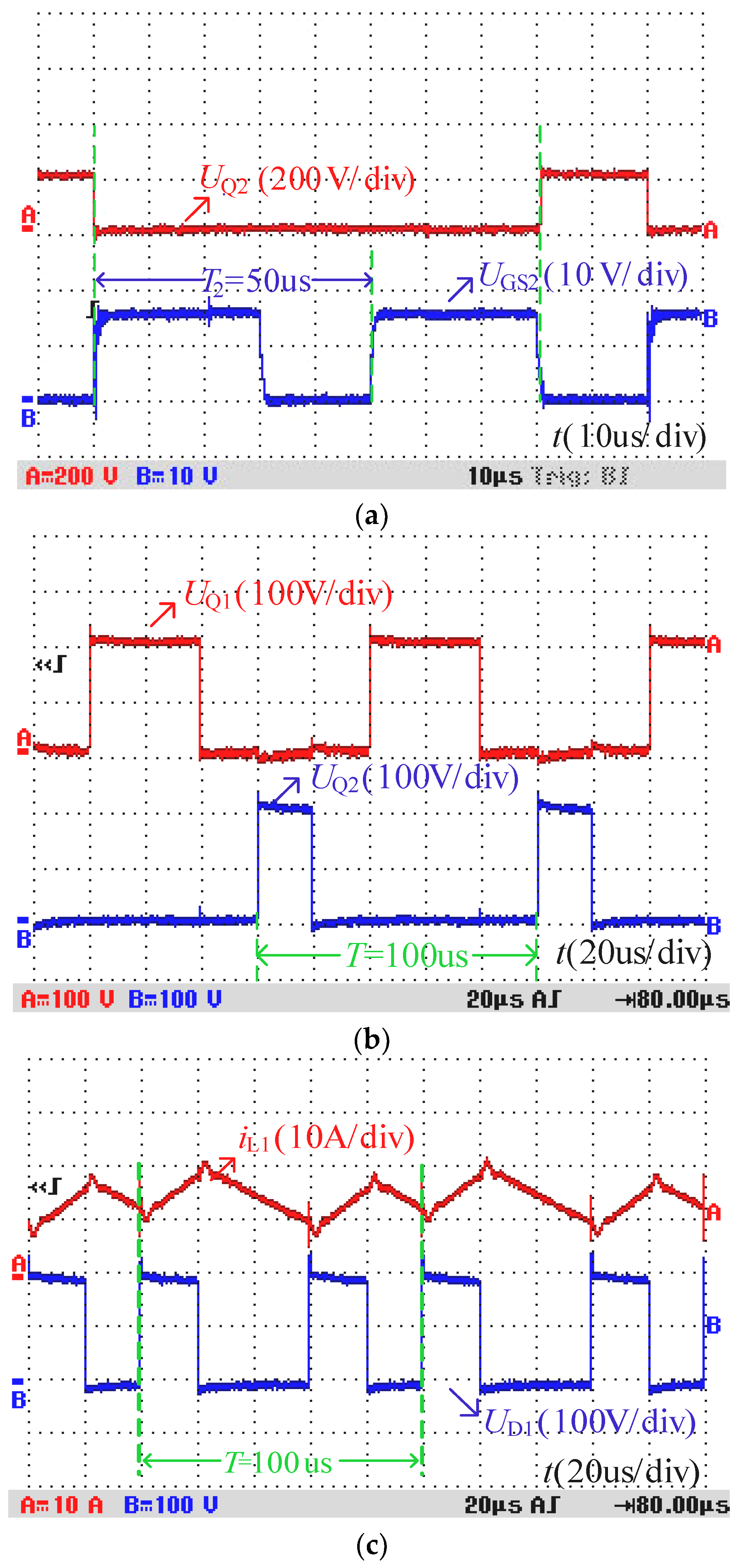
3.2. Comparisons of Voltage and Current Stresses

In Table 1, the voltage stress across the components in BTL-qZ converter controlled by the proposed and the original modulation strategies is compared, when the voltage gain M and the output voltage UO are under the same conditions, respectively. According to Table 1, the theoretical voltage stress across the corresponding capacitors and the power semiconductors in BTL-qZ converter controlled by the two modulation strategies are all equal. Hence, the proposed modulation strategy still retains the advantage of the low component voltage stress for the BTL-qZ converter.
In Table 2, the current stress on the components for BTL-qZ converter controlled by the proposed and the original modulation strategies is compared, when the voltage gain M and the output current IO are under the same conditions, respectively. According to Table 2, the theoretical current stresses on the corresponding power switches for BTL-qZ converter controlled by the two modulation strategies are equal to 2MIO. However, the theoretical current stress on D1 under the proposed modulation strategy is 2MIO, which is higher than the original modulation strategy. In addition, the corresponding theoretical current stresses on D2 and D3 under the two modulation strategies can also be obtained, which are equal respectively. Therefore, it is easy to choose the diodes with the same rated parameters. However, the theoretical current stress for the proposed modulation strategy is higher than that of the original modulation strategy. Hence, the current stresses on diodes under the proposed modulation strategy are all greater than those of the original modulation strategy.

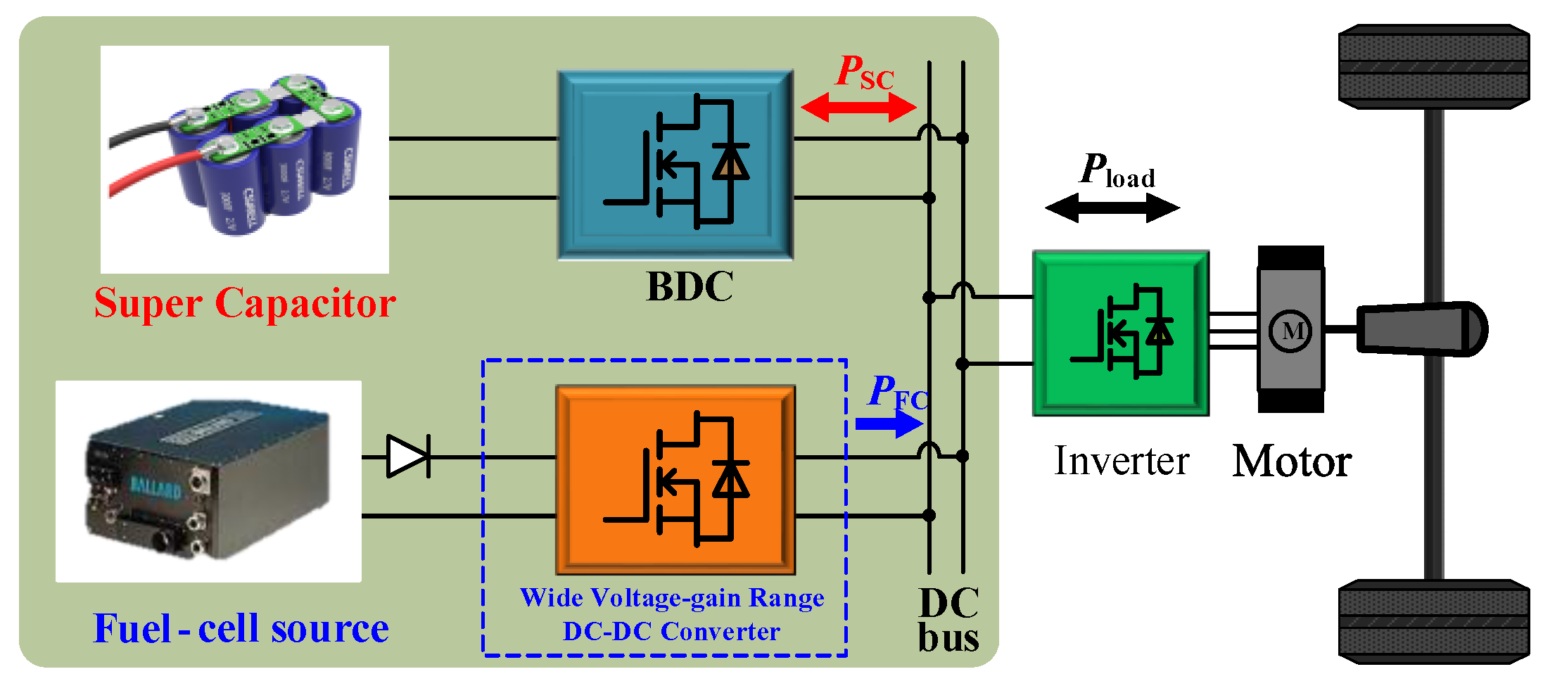
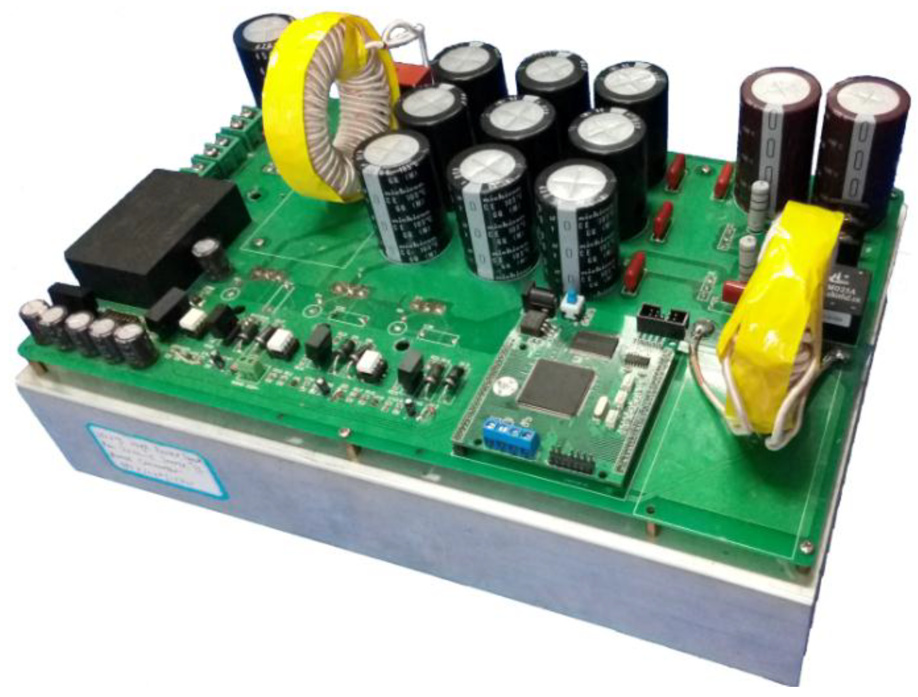
4. Application of the Converter for Fuel Cell Vehicles

On the basis of the output characteristic of the fuel cell presented previously, the powertrain of fuel cell vehicles with the required converters is shown in Figure 6. The energy sources consist of the fuel-cell source and the super capacitor. The low voltage of the fuel-cell source is boosted to match the high voltage of the DC bus by a wide voltage-gain range DC-DC converter. At the same time, the fuel-cell source provides the average power (PFC) for the DC bus. The super capacitor is deployed to supply the instantaneous peak power (PSC) required due to the slow dynamic response of the fuel-cell source, and to absorb the power recovery from the DC bus by the bidirectional DC-DC converter (BDC). Accordingly, the power interface between the fuel-cell source and the DC bus should have a wide voltage-gain range characteristic, as well as a high voltage-gain feature. When the fuel cell vehicle operates at a constant speed, the fuel-cell source provides the stable energy for the load (Pload), and charges the super capacitor if it is needed. When the fuel cell vehicle accelerates, the super capacitor supplies the instantaneous power required from the motor. Then the fuel-cell source can increase its output power gradually, and ensure the vehicle still has the fast dynamic response. When the fuel cell vehicle decelerates or brakes, the fuel-cell source decreases its output power, and the super capacitor absorbs the regenerative energy.

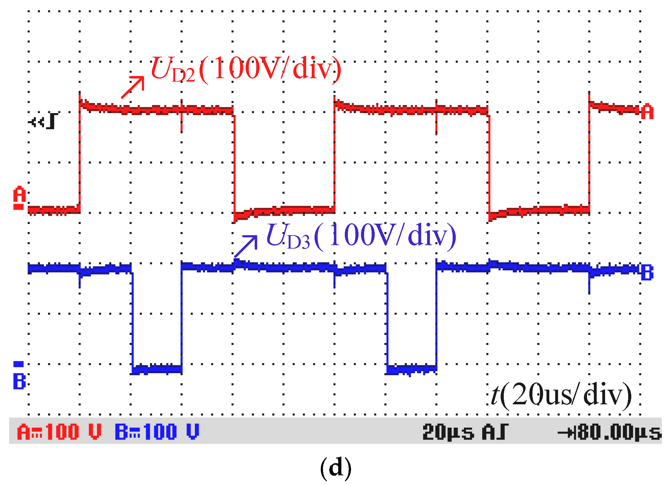
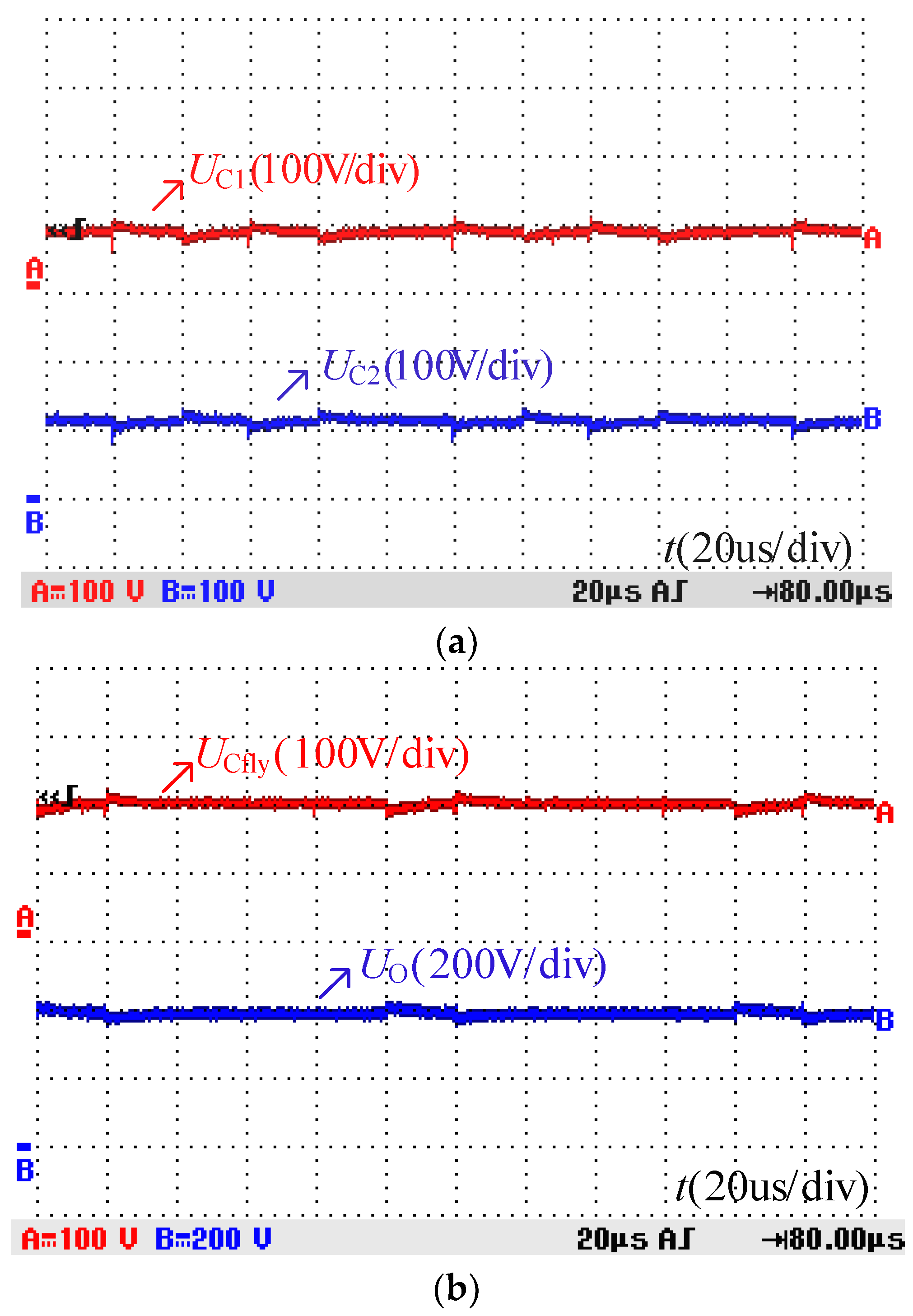
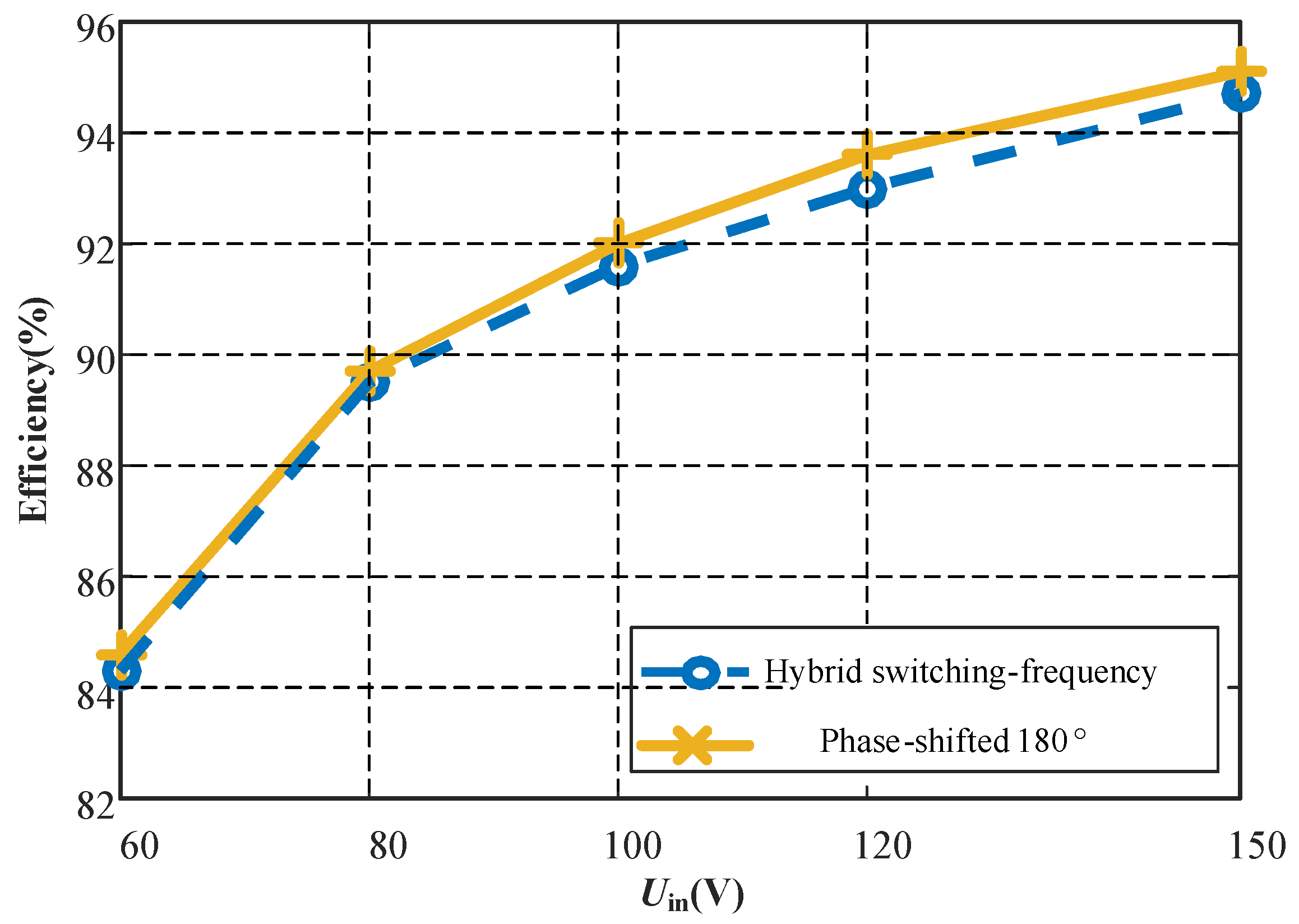
5. Experimental Results and Analysis

In order to validate the operating performance of the BTL-qZ converter controlled by the proposed modulation strategy, a BTL-qZ experimental prototype is developed as shown in Figure 7. The parameters of this prototype are the same as those in [34], which are listed in Table 3.
The gate signals of Q1 and Q2 and inductor currents of L1 and L2 with the two modulation strategies are shown in Figure 8, when the voltage gain is M = 10 and the output voltage is UO = 400 V. For the original modulation strategy, as shown in Figure 8a, the frequencies of the gate signals for both Q1 and Q2 are 10 kHz. As to the proposed modulation strategy, as shown in Figure 8b, the frequencies of the gate signal for Q2 is 20 kHz. According to Figure 8, the duty cycles of Q1 and Q2 are both the same with the two modulation strategies, but different duty cycles are needed for achieving the voltage gain 10. As a result, the duty cycles 0.7 for the original modulation strategy, and the duty cycles 0.6 for the proposed modulation strategy are required respectively, which agree with the theoretical analysis. Comparing with these duty cycles, the conclusion that the proposed modulation strategy can avoid extreme duty cycles better than the original modulation strategy, under the same condition of the high step-up voltage-gain can be achieved.
Inductor currents of L1 and L2 with the two modulation strategies are shown in Figure 8c,d, when the output voltage is UO = 400 V and the load is R = 400 Ω. From Figure 8c, the current ripple rates and the frequencies of iL1 and iL2 are about 62.07% and 20 kHz, respectively. Therefore, the equivalent frequency of the inductor current is double the switching frequency. According to Figure 8d, the current ripple rates of iL1 and iL2 are about 66.67%. Although the frequency of iL1 and iL2 are 10 kHz, the inductor can charge and discharge twice in each switching period of Q1, respectively. In addition, the charging time is identical, but the discharging time is different. So the approximate current ripple can be achieved under the proposed modulation strategy, comparing with the original modulation strategy.
The gate signal and the voltage stress across Q2 are shown in Figure 9a, when the voltage gain is M = 10 and the output voltage is UO = 400 V. According to Figure 9a, although the frequency of the gate signal for Q2 is 20 kHz, the frequency of the voltage stress across Q2 is still 10 kHz, which agrees with the theoretical analysis of the hybrid switching-frequency modulation strategy mentioned in Figure 4c,e.
The voltage stress across the power semiconductors and the capacitors with the two modulation strategies are shown in Figure 9 and Figure 10, when the output voltage is UO = 400 V and the voltage gain is M = 10. From Figure 9b–d, it can be observed that the voltage stress across all the power semiconductors is 200 V. According to Figure 10a, the voltage stresses across C1 and C2 are 80 V and 120 V respectively. From Figure 10b, the voltage stress across Cfly is 200 V (i.e., half of the output voltage) approximately. Therefore, these experimental results validate the correctness of the theoretical analysis of the voltage stress across the power semiconductors and the corresponding capacitors with the two modulation strategies respectively. When the output voltage is UO = 400 V and the load resistance is R = 400 Ω, the efficiency η measured by a power analyser (WT3000, Yokogawa, Tokyo, Japan) for different input voltages varying from 150 V to 60 V under the two modulation strategies is shown in Figure 11. It is noticed that when the input voltage declines, the efficiency decreases correspondingly due to the increasing losses caused by the increasing input current. The maximum measured efficiencies of the BTL-qZ converter controlled by the original and proposed modulation strategies are 95.1% and 94.7% respectively, which are approximately equal. However, the minimum measured efficiencies of the BTL-qZ converter controlled by the proposed modulation strategy is 86.3% which is 1.7% higher than that with the original modulation strategy in [34].

6. Conclusions

An enhanced hybrid switching-frequency modulation strategy is proposed for the boost three-level DC-DC converter with a quasi-Z source (BTL-qZ) employed in fuel cell vehicles. The proposed modulation strategy retains many advantages of the phase-shifted 180-degree modulation strategy, such as the low input current ripple, the low voltage stress across the power semiconductors, and the controllable voltage across the flying capacitor. In addition, compared with the phase-shifted 180-degree modulation strategy, the BTL-qZ converter controlled by the proposed modulation strategy can achieve a higher voltage gain range, with the more proper duty cycles [1/3, 2/3) for the power switches rather than [1/2, 3/4), which can avoid the extreme duty cycles better than the original modulation strategy. Therefore, it is beneficial for the BTL-qZ converter to interface the wide voltage range fuel cell source and the high voltage DC bus in fuel cell vehicles.

Author Contributions

Yun Zhang, Jilong Shi and Mark Sumner conceived and designed the experiments; Chuanzhi Fu performed the experiments; Jilong Shi and Ping Wang analyzed the data; Jing Li contributed reagents/materials/analysis tools; Yun Zhang, Chuanzhi Fu and Wei Zhang wrote the paper.

Conflicts of Interest

The authors declare no conflict of interest.

Nomenclature

L1, L2Inductances of the inductors in the quasi-Z source.
C1, C2, C3, CflyCapacitances of the capacitors in the quasi-Z source, the output capacitor and the flying capacitor.
PThe rated power of the converter.
RThe load resistance.
M1, M2The step-up voltage-gains of the BTL-Qz DC-DC converter with the 180-degree modulation phase-shifted strategy and the enhanced hybrid switching-frequency modulation strategy.
mThe modulation index of power switches Q1 and Q2.
UCflyThe voltage across the flying capacitor in the converter.
UC1, UC2The voltages across the capacitors in the quasi-Z source.
UQ1, UQ2The voltage stresses across power switches Q1 and Q2.
UD1, UD2, UD3The voltage stresses across diodes D1, D2 and D3.
t1-t4The durations of the corresponding switching states.
fThe carrier frequency of the gate signal Q1.
Uin, UOThe input and output voltages of the converter.
UGS1, UGS2The gate signals of power switches Q1 and Q2.
iL1, iL2The inductor currents of L1 and L2.

References

  1. Migliardini, F.; Capasso, C.; Corbo, P. Optimization of hydrogen feeding procedure in PEM fuel cell systems for transportation. Int. J. Hydrogen Energy 2014, 39, 21746–21752. [Google Scholar] [CrossRef]
  2. Veneria, O.; Capassoa, C.; Patalano, S. Experimental investigation into the effectiveness of a super-capacitor based hybrid energy storage system for urban commercial vehicles. Appl. Energy 2017. [CrossRef]
  3. Omar, N.; Daowd, M.; Hegazy, O.; Bossche, P.; Coosemans, T.; Mierlo, J. Electrical double-layer capacitors in hybrid topologies—Assessment and evaluation of their performance. Energies 2012, 5, 4533–4568. [Google Scholar] [CrossRef]
  4. Gopinath, R.; Kim, S.; Hahn, J.H.; Enjeti, P.N.; Yeary, M.B.; Howze, J.W. Development of a low cost fuel cell inverter system with DSP control. IEEE Trans. Power Electron. 2004, 19, 1256–1262. [Google Scholar] [CrossRef]
  5. Palma, L.; Enjeti, P.N. A modular fuel cell, modular DC–DC converter concept for high performance and enhanced reliability. IEEE Trans. Power Electron. 2009, 24, 1437–1443. [Google Scholar] [CrossRef]
  6. Pagano, M.; Piegari, L. Electrical networks fed by fuel-cells for uninterruptible electrical supply. In Proceedings of the IEEE International Symposium on Industrial Electronics-ISIE, L’Ayuila, Ttaly, 8–11 July 2002; pp. 953–958. [Google Scholar]
  7. Tekin, M.; Hissel, D.; Pera, M.C.; Kauffmann, J.M. Energy-management strategy for embedded fuel-cell systems using fuzzy logic. IEEE Trans. Ind. Electron. 2007, 54, 595–603. [Google Scholar] [CrossRef]
  8. Jia, J.; Wang, G.; Cham, Y.T.; Wang, Y.; Han, M. Electrical characteristic study of a hybrid PEMFC and ultracapacitor system. IEEE Trans. Ind. Electron. 2010, 57, 1945–1953. [Google Scholar]
  9. Prasanna, U.R.; Rathore, A.K. Dual three-pulse modulation-based high-frequency pulsating DC link two-stage three-phase inverter for electric/hybrid/fuel cell vehicles applications. IEEE J. Emerg. Sel. Top. Power Electron. 2014, 2, 477–486. [Google Scholar] [CrossRef]
  10. Su, G.; Tang, L. A reduced-part, triple-voltage DC–DC converter for EV/HEV power management. IEEE Trans. Power Electron. 2009, 24, 2406–2410. [Google Scholar]
  11. Pera, M.C.; Candusso, D.; Hissel, D.; Kauffmann, J.M. Power Generation by Fuel Cells. IEEE Ind. Electron. Mag. 2007, 1, 28–37. [Google Scholar] [CrossRef]
  12. Shen, M.; Joseph, A.; Wang, J.; Peng, F.Z.; Adams, D.J. Comparison of Traditional Inverters and Z-Source Inverter for Fuel Cell Vehicles. IEEE Trans. Power Electron. 2007, 22, 1453–1463. [Google Scholar] [CrossRef]
  13. Fontes, G.; Turpin, C.; Astier, S. A Large-Signal and Dynamic Circuit Model of a H2/O2 PEM Fuel Cell: Description, Parameter Identification, and Exploitation. IEEE Trans. Ind. Electron. 2010, 57, 1874–1881. [Google Scholar] [CrossRef]
  14. Martins, G.M.; Pomilio, J.A.; Buso, S.; Spiazzi, G. Three-phase low frequency commutation inverter for renewable energy systems. IEEE Trans. Ind. Electron. 2006, 53, 1522–1528. [Google Scholar] [CrossRef]
  15. Wai, R.J.; Lin, C.Y.; Duan, R.Y.; Chang, Y.R. High-efficiency DC–DC converter with high voltage gain and reduced switch stress. IEEE Trans. Ind. Electron. 2007, 54, 354–364. [Google Scholar] [CrossRef]
  16. Todorovic, M.H.; Palma, L.; Enjeti, P.N. Design of a Wide Input Range DC–DC Converter with a Robust Power Control Scheme Suitable for Fuel Cell Power Conversion. IEEE Trans. Ind. Electron. 2008, 55, 1247–1255. [Google Scholar] [CrossRef]
  17. Shahin, A.; Hinaje, M.; Martin, J.; Pierfederici, S.; Raël, S.; Davat, B. High Voltage Ratio DC–DC Converter for Fuel-Cell Applications. IEEE Trans. Ind. Electron. 2010, 57, 3944–3955. [Google Scholar] [CrossRef]
  18. Zhang, M.T.; Jiang, Y.; Lee, F.C.; Jovanovic, M.M. Single-phase three-level boost power correction converter. Proc. APEC 1995, 1, 434–439. [Google Scholar]
  19. Fontes, G.; Turpin, C.; Astier, S.; Meynard, T. Interactions between fuel cell and power converters: Influence of current harmonics on a fuel cell stack. IEEE Trans. Power Electron. 2007, 22, 670–678. [Google Scholar] [CrossRef]
  20. Kwon, J.M.; Kim, E.H.; Kwon, B.H.; Nam, K.H. High-efficiency fuel cell power conditioning system with input current ripple reduction. IEEE Trans. Ind. Electron. 2009, 56, 826–834. [Google Scholar] [CrossRef]
  21. Tseng, K.C.; Liang, T.J. Novel high-efficiency step-up converter. Proc. Inst. Electr. Eng. Electr. Power Appl. 2004, 151, 182–190. [Google Scholar] [CrossRef]
  22. Prudente, M.; Pfitscher, L.L.; Emmendoerfer, G.; Romaneli, E.F.; Gules, R. Voltage Multiplier Cells Applied to Non-Isolated DC–DC Converters. IEEE Trans. Power Electron. 2008, 23, 871–887. [Google Scholar] [CrossRef]
  23. Zhao, Q.; Lee, F.C. High-efficiency, high step-up DC–DC converters. IEEE Trans. Power Electron. 2003, 18, 65–73. [Google Scholar] [CrossRef]
  24. Graditi, G.; Adinolfi, G.; Tina, G.M. Photovoltaic optimizer boost converters: Temperature influence and electro-thermal design. Appl. Energy 2014, 115, 140–150. [Google Scholar] [CrossRef]
  25. Peng, F.Z.; Li, H.; Su, G.; Lawler, J.S. A new ZVS bidirectional DC–DC converter for fuel cell and battery application. IEEE Trans. Power Electron. 2004, 19, 54–65. [Google Scholar] [CrossRef]
  26. Amodeo, S.J.; Chiacchiarini, H.G.; Oliva, A.R. High-performance control of a DC–DC Z-source converter used for an excitation field river. IEEE Trans. Power Electron. 2012, 27, 2947–2957. [Google Scholar] [CrossRef]
  27. Anderson, J.; Peng, F.Z. A class of quasi-Z-source inverters. In Proceedings of the IEEE Industry Applications Society Annual Meeting, Edmonton, AB, Canada, 5–9 October 2008; pp. 1–7. [Google Scholar]
  28. Yang, S.; Peng, F.Z.; Lei, Q.; Inoshita, R.; Qian, Z. Current-fed quasi-Z-source inverter with voltage Buck–Boost and regeneration capability. IEEE Trans. Ind. Appl. 2011, 47, 882–892. [Google Scholar] [CrossRef]
  29. Ellabban, O.; Abu-Rub, H.; Ge, B. A quasi-Z-source direct matrix converter feeding a vector controlled induction motor drive. IEEE J. Emerg. Sel. Top. Power Electron. 2015, 3, 1063–1072. [Google Scholar] [CrossRef]
  30. Patidar, K.; Umarikar, A.C. High step-up pulse-width modulation DC–DC converter based on quasi-Z-source topology. IET Power Electron. 2015, 8, 477–488. [Google Scholar] [CrossRef]
  31. Ruan, X.; Li, B.; Chen, Q.; Tan, S.; Tse, C.K. Fundamental considerations of three-level DC–DC converters: Topologies, analyses, and control. IEEE Trans. Circuits Syst. I Reg. Papers 2008, 55, 3733–3743. [Google Scholar] [CrossRef]
  32. Chen, H.; Liao, J. Design and implementation of sensorless capacitor voltage balancing control for three-level Boosting PFC. IEEE Trans. Power Electron. 2014, 29, 3808–3817. [Google Scholar] [CrossRef]
  33. Dusmez, S.; Hasanzadeh, A.; Khaligh, A. Comparative analysis of bidirectional three-level DC–DC converter for automotive applications. IEEE Trans. Ind. Electron. 2015, 62, 1063–1072. [Google Scholar] [CrossRef]
  34. Zhang, Y.; Shi, J.; Zhou, L.; Li, J.; Sumner, M.; Wang, P.; Xia, C. Wide Input-Voltage Range Boost Three-Level DC-DC Converter with Quasi-Z Source for Fuel Cell Vehicles. IEEE Trans. Power Electron. 2017, 32, 6728–6738. [Google Scholar] [CrossRef]
Figure 1. Boost three-level DC-DC converter with quasi-Z source (BTL-qZ) for fuel cell vehicles in [34].
Energies 11 01026 g001
Figure 2. Key waveforms of the BTL-qZ converter controlled by phase-shifted 180-degree modulation strategy. (a) Modulation wave and carriers; (b) Gate signal of Q1; (c) Gate signal of Q2; (d) Voltage stress across Q1; (e) Voltage stress across Q2; (f) Capacitor voltage across C1; (g) Capacitor voltage across C2; (h) Capacitor voltage across C3; (i) Voltage stress across D1; (j) Voltage stress across D2; (k) Voltage stress across D3; (l) Inductor current of L1; and (m) Inductor current of L2.
Energies 11 01026 g002
Figure 3. Energy flow paths of the BTL-qZ converter in different switching states. (a) S1S2 = 11; (b) S1S2 = 01; (c) S1S2 = 00; (d) S1S2 = 10.
Energies 11 01026 g003aEnergies 11 01026 g003b
Figure 4. Key waveforms of the BTL-qZ converter controlled by hybrid switching-frequency modulation strategy. (a) Modulation wave and carriers; (b) Gate signal of Q1; (c) Gate signal of Q2; (d) Voltage stress across Q1; (e) Voltage stress across Q2; (f) Capacitor voltage across C1; (g) Capacitor voltage across C2; (h) Capacitor voltage across C3; (i) Voltage stress across D1; (j) Voltage stress across D2; (k) Voltage stress across D3; (l) Inductor current of L1; and (m) Inductor current of L2.
Energies 11 01026 g004
Figure 5. Comparisons of voltage gain versus modulation index for different modulation strategies.
Energies 11 01026 g005
Figure 6. Powertrain of fuel cell vehicles.
Energies 11 01026 g006
Figure 7. Experimental prototype.
Energies 11 01026 g007
Figure 8. Gate signals of Q1 and Q2 and inductor currents of L1 and L2 with two modulation strategies. (a) Gate signals of Q1 and Q2 with phase-shifted 180-degree; (b) Gate signals of Q1 and Q2 with hybrid switching-frequency; (c) Inductor currents of L1 and L2 with phase-shifted 180-degree; (d) Inductor currents of L1 and L2 with hybrid switching-frequency.
Energies 11 01026 g008aEnergies 11 01026 g008b
Figure 9. Experimental waveforms of gate signals, voltage stresses and inductor currents with hybrid switching-frequency modulation strategy. (a) Gate signal and voltage stress across Q2; (b) Voltage stresses across Q1 and Q2; (c) Inductor current of L1 and voltage stress across D1; (d) Voltage stresses across D2 and D3.
Energies 11 01026 g009aEnergies 11 01026 g009b
Figure 10. Experimental waveforms of capacitor voltages with two modulation strategies. (a) Voltage stress across Capacitors C1 and C2 with hybrid switching-frequency modulation strategy; (b) Voltage stress across Capacitors Cfly and output voltage UO in hybrid switching-frequency modulation strategy.
Energies 11 01026 g010
Figure 11. Compared efficiencies with different input voltages with two modulation strategies.
Energies 11 01026 g011
Table 1. Comparisons of voltage stress for components in BTL-qZ converter controlled by proposed and original modulation strategies respectively.
Modulation StrategyC1C2CflyQ1Q2D1D2D3
Phase shifted 180-degree M 2 4 M U O M + 2 4 M U O UO/2UO/2UO/2UO/2UO/2UO/2
hybrid switching-frequency M 2 4 M U O M + 2 4 M U O UO/2UO/2UO/2UO/2UO/2UO/2
Table 2. Comparisons of current stress for components in BTL-qZ converter controlled by proposed and original modulation strategies respectively.
Modulation StrategyQ1Q2D1D2D3
Phase-shifted 180-degree2MIO2MIO ( 2 M 4 M M + 2 ) × I O 4 M M + 2 I O 4 M M + 2 I O
hybrid switching-frequency2MIO2MIO2MIO 6 M M + 2 I O 6 M M + 2 I O
Table 3. Main experimental parameters of the BTL-qZ converter in [34].
Parameters and ComponentsValues (units)
Input voltage Uin40~150 V
Output voltage UO400 V
Inductor L1228 μH
Inductor L2225 μH
Capacitors C1, C2 and Cfly450 V/660 μF
Capacitor C3450 V/440 μF
Rated power P400 W
Load R400 Ω
MOSFETs Q1 and Q2IXTK102N30P
Diodes DFC, D1, D2 and D3DSEC60-03A

