A Novel Three-Level Voltage Source Converter for AC–DC–AC Conversion
by
 ,
,
Zongbin Ye
1,2,* ,
,
Anni Chen
1,2,
Shiqi Mao
1,2,
Tingting Wang
1,2,
Dongsheng Yu
1,2 and
Xianming Deng
1,2 1
Jiangsu Province Laboratory of Mining Electric and Automation, China University of Mining and Technology, Xuzhou 221008, China
2
School of Electrical and Power Engineering, China University of Mining and Technology, Xuzhou 221008, China
*
Author to whom correspondence should be addressed.
Energies 2018, 11(5), 1147; https://doi.org/10.3390/en11051147
Submission received: 26 March 2018
/
Revised: 26 April 2018
/
Accepted: 27 April 2018
/
Published: 4 May 2018
(This article belongs to the Special Issue Multilevel Converters: Analysis, Modulation, Topologies, and Applications)
Abstract
:This paper presents a novel three-level voltage source converter for AC–DC–AC conversion. The proposed converter based on H-bridge structure is studied in detail. The control method with traditional double-closed-loop control strategy and voltage balancing algorithm is applied to the rectifier side. Correspondingly, a simplified modulation algorithm is applied to the inverter side, and the voltage balancing of inverter side is realized through the optimal selection of switching combination. Then, the application of the proposed topology is assessed in general and ideal operation conditions. Furthermore, the proposed topology with a variable voltage variable frequency (VVVF) is verified in experimental conditions. The performance of the proposed converter and control strategy is evaluated by experimental and simulation results.
1. Introduction
With the development of the multilevel converter (MC), it has become a cost-effective solution of medium-voltage AC drives [1]. Due to its merits compared with a conventional two-level voltage source converter—such as lower voltage stress on switches, improved output waveforms, reduced common mode voltage, and high voltage capability—MC has been applied to more emerging fields [2,3,4]. The areas of applications include renewable energy generation, electric vehicle traction [5], high-power energy storage system [6], micro-grids [7], high-voltage ac or dc transmission [8,9,10], and some newly-developing fields.
In general, there are two conventional types of AC–DC–AC multilevel converters in view of whether it has common dc-links. The diode-clamped MC (DCMC) [11] and fly-capacitor MC (FCMC) [12] are widespread adopted structures with common dc-links, which can operate in four quadrants and be supplied by single rectifier. Besides, there are some other topologies, such as five-level active neutral-point-clamped MC (5L-ANPC) [13], modular MC (MMC) [9,10], and some newly-developed MC [14,15,16]. However, these kinds of MCs, except MMC, are hard to extend towards higher output voltage levels and power grades because of the complicated structures. The other drawback of these types is the poor ability to deal with some special systems which have different voltage grades, e.g., connection of two grids with different voltage grades [16,17,18]. Separated dc-links are the features of the other types of MCs, including cascaded H-bridge MC (CHBMC) [17], five-level H-bridge NPC (5L-HNPC) [18], and some hybrid and asymmetrical cascaded H-bridge MCs with different sub-modules [19] or dc-link voltages [20]. It has the advantage of flexible extending of the output levels and power rating. However, the bulky and expensive phase-shifting transformers for isolated dc sources make it hard to increase the power density. A back-to-back CHB converter without any isolating device [21] can avoid these problems. However, short-circuits caused by the hardware topology are difficult to solve and the proposed topology cannot be expanded to a three phase system.
In this paper, a new three-level voltage source converter for AC–DC–AC conversion is proposed. It can be used in three-phase system and more easily to extend to higher voltage level than a back-to-back NPC converter. Compared to the back-to-back CHB converter proposed in [21], a half H-bridge cell used in the new topology provides more redundant vectors and makes it overcome the short-circuit problem, which simplifies the control method. In addition, the proposed topology utilizes fewer switches at the cost of increasing the number of dc-link capacitors, the separated dc links will decrease the total dc voltage of the system, which is beneficial for the insulation design in many fields [22].
The rest of the paper is organized as follows. In Section 2, the circuit configuration, characteristics and working principles of the proposed topology are studied in detail. The overall control strategy and pulse-width modulation strategy considering the voltage balance control is given in Section 3. In Section 4, two operation conditions are analyzed, and the simulation and experimental results demonstrate the effectiveness of the proposed control strategies. Section 5 concludes the paper.
2. Circuit Configuration of Proposed Three-Level Voltage Source Converter
2.1. Circuit Configuration
The proposed three-level converter is presented in Figure 1. It includes two basic submodules, power unit I and power unit II. Port 2 of power unit II in the three-phase topology is connected together, forming the neutral point N of the converter.
For convenience, the rectifier side, common part, inverter side I, and inverter side II can be defined as shown in Figure 1. The rectifier side connects in series with three-phase inductors and the grid through three phase electrical terminals A, B, and C. The three electrical terminals A, B, and C of inverter side connect with the three-phase load.
2.2. Working Principle of Rectifier Side
All the dc-link voltage values are assumed to be equal to Udc. Obviously, the output voltage levels relative to neutral point N are determined by and . uX_rec (X = A, B, C) is defined as the output voltage of rectifier side, which can be obtained as Equation (1).
2.3. Working Principle of Inverter Side I
Combined with the common parts shown in Figure 1, inverter side I can produce three level voltages similar to uX_rec. uX_inv referenced to N is obtained as Equation (2).
2.4. Master–Slave Control Principle
Combining with common part, there will be no problem obviously when rectifier side or inverter side I works independently. Due to the special structure, the operation principle of each side cannot be analyzed independently when they work together. In other words, there is a coupling relationship between two sides. Since any side can be chosen as the master control side, the rectifier side is chosen as an example. Hence the switching command of S2 is decided by rectifier side. Output voltage levels of uX_inv will be limited in some switching combinations. For example, if rectifier side is P, S2 should be 0. However, if the inverter side I needs to be N, S2 should be 1. Consequently, a contradiction appears.
In order to reduce the coupling relationship, a submodule power unit I is added on the right of power unit II, which is defined as inverter side II, as shown in Figure 1. According to the switching states, the switching commands of S3S4S5 can be decided after switching commands of S1S2 are generated as shown in Table 1. The output voltage of inverter side, uX_inv can be rewritten as Equation (3).
2.5. Comparison with Classic Multilevel Topologies
For better understanding of the proposed technology, it is necessary to make a comparison over classic multilevel converter topologies. In order to achieve four-quadrant AC–DC–AC conversion, NPC, FC, and CHB are arranged in a back-to-back (B2B) scheme [23]. As a matter of convenience, the proposed topology is abbreviated as CMC. The state-of-the-art 4.5 kV, 450 A and 3.3 kV, 450 A IGBTs are applied in aforementioned three level and five level topologies, respectively, with the output line-to-line voltage Vll_rms = 3 kV and power rating of 600 kW. It is assumed that the voltage rating of each clamping diode and flying capacitor is equal to the main switch device voltage rating. A comprehensive list of the requested components number of each converter topology is shown in Table 2 [24,25]. Obviously, the counts of active devices of these types are equal except the CMC, which needs two extra switches in each phase. A total of 36 diodes are requested in a five level B2B NPC converter, and the count will increase dramatically with the number of levels. Capacitors contain dc-link capacitors and flying capacitors, so the number of capacitors—as an example—for 5L B2B FC topology is 4 + 18. These large numbers of capacitors increase size and cost of the converter and reduce the reliability. Through the total component amount, CHB topology is extremely advantageous in quantity in the Table, but it must be equipped with a transformer and PWM rectifier for four-quadrant applications. In the rest of the topologies, CMC topology, without clamping diodes and capacitors, has a lower number of components than other topologies with the improvement of voltage level.
To compare with the B2B 3L-NPC, the switching losses for both topologies are calculated and normalized according to the method proposed in [26] and the datasheet of IGBT. The result is shown in Figure 2 where the modulation index of the inverter side ranges from 0.5 to 1.15 and the power factor of the load ranges from 0.7 to 1.
3. Control Method of the Proposed Three-Level Voltage Source Converter
3.1. Control Method
Since this work focuses on testing the proposed three-level converter topology, a common control method should be used. So dual close loop control structure in d–q synchronous reference frame is adopted in rectifier side [20]. The voltage loop contains a conventional proportional-integral (PI) controller to regulate the average value of capacitor voltage of CX_rec, Udc_ave_rec to reference value Udcref_rec (=Udc). The reference current of the q-axis (i*q) is set to a certain value to adjust input power factor of the whole converter. Then, the inner current loops generate the reference voltage of rectifier side, u*X_rec. Subsequently, the zero sequence voltage uz_rec generated by the voltage balancing algorithm is injected to u*X_rec to control voltage values of CX_rec. Then a simplified modulation algorithm in [27] is adopted to calculate the duration time of switching states, P/O/N, in the rectifier side and inverter side.
Due to the coupling relationship, proper switching commands of S2/S3/S4/S5 should be chosen to achieve voltage balancing of the capacitors CX_inv. The optimal selection of switching combination (OSSC) is introduced later to generate the converter switching commands of S1~S5. The whole control block diagram of the proposed three-level converter is shown in Figure 3.
3.2. Modulation Algorithm
A simplified PWM strategy [27] which is easier and more flexible to realize different targets was used as modulation algorithm. Taking inverter side as an example and assuming that Udcref_inv = Udc, uX_inv(t) consists of Udc and 0 when the reference voltage u*X_inv > 0; otherwise, uX_inv(t) consists of −Udc and 0. This divides the space vector diagram into six sectors, as denoted by S in Figure 4.
When S = 1, the voltage-second balancing principle can be represented by Equation (4), where uz represents the equivalent zero-sequence voltage. The general solutions of (4) can be obtained as Equation (5).
TX_inv stands for the duration time of switching state P when (u*X_inv − uz > 0) otherwise stands for the duration time of O.
3.3. Voltage Balancing Algorithm of Rectifier Side
There is only one capacitor in each phase. It only needs to consider the voltage balancing of CX_rec between three-phase. Assuming that uz_rec is the zero sequence voltage injected into u*X_rec, which is used to realize the targets of voltage balancing of CX_rec. The voltage-second balancing principle can be represented by Equation (6).
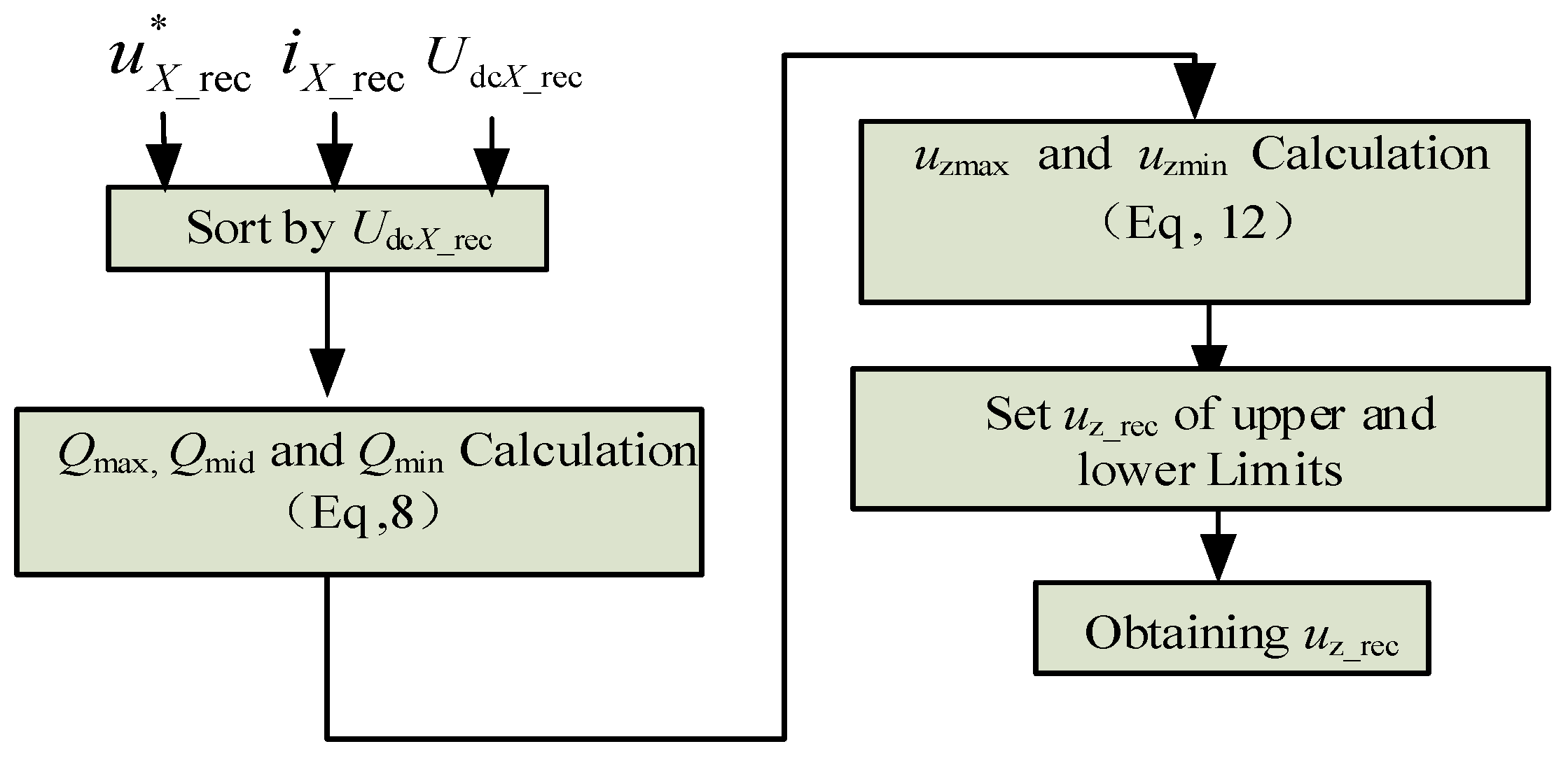
If UdcX_rec is imbalanced, uz_rec should be calculated to adjust the reference voltage u*X_rec. As an example, if voltage values of CX_rec satisfy UdcA_rec > UdcB_rec > UdcC_rec, it means that the magnitude of charge change within Ts should be QA < QB < QC. uz_rec can be changed to adjust QX. Calculation of uz_rec is as follows:
- QX, u*X_rec, and iX_rec are sorted according to UdcX_rec. In order to realize the voltage balancing, QX should satisfy Equation (7).QX is defined as Equation (8).If iX_rec > 0 and (u*X_rec − uz_rec) > 0, uX_rec consists of P/O. The current paths of S1S2 are shown in Figure 5. Obviously, QX > 0 and CX_rec is charged in this case. CX_rec is discharged within Ts when iX_rec < 0 and (u*X_rec − uz_rec) > 0.
- Substituting (8) into (7) gives (9).utemp1 = b1/a1, and utemp2 = b2/a2.
- The range of uz_rec can be obtained from Equation (9), and uz_rec can take any value within the range. However, it should satisfy Equation (11) to acquire a linear modulation.
- Calculating the limit value of uz_rec: the corresponding limitations of the injected zero-sequence voltages are given in (12).
3.4. Voltage Balancing Method of Inverter Side
Maintaining voltage balancing of the flying-capacitors in the inverter side is the main aim of this section. As introduced before, the coupling relationship shown in Table 1 can provide considerable number of redundant switching combinations. These combinations can provide a charging or discharging current paths for each flying-capacitors. The voltage balance control can be realized by selecting a proper combination. The optimal selection of switching combination can be generated as follows.
3.4.1. Effect of the Switching States on the Capacitors Voltages
According to Equation (3), the switching states of the inverter side P/O/N can be generated by inverter side I or II. However, only the switching states produced by inverter side II (S4S5) have an effect on the capacitors voltages UdcX_inv. Which inverter side is selected to generate the required switching states is decided by the inverter state, the direction of iX_inv, and switching commands of S2 as listed in Table 4.
3.4.2. Optimal Selection of Switching Combination (OSSC)
To balance the voltage of CX_inv, OSSC is set to select proper switching combinations after the previous step (1). Before selecting the switching combination, the duration of switching state (TX_rec/TX_inv) is calculated through the simplified modulation algorithm in [27], thus the inverter state and rectifier state are determined. The switching commands of S2 should be a certain state 0(1) if the rectifier side is P(N). While it cannot be decided when rectifier side is O. Based on the actual situation, iX_inv can be measured. To analyze the working principle of OSSC, the two examples are listed.
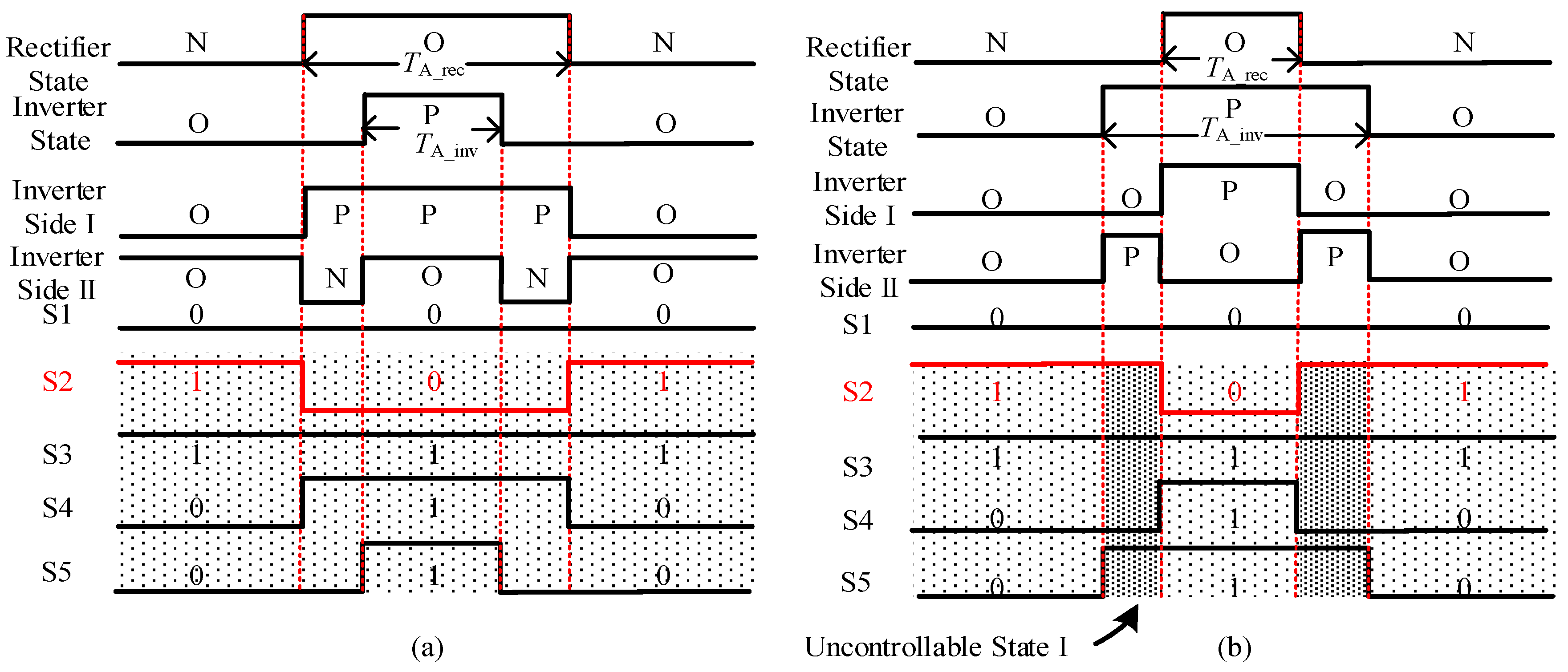
Condition I: UdcA_inv should be decreased with a proper switching combination. Referring to Table 4, when the switching state of the rectifier and inverter sides are N (S2 = 1) and O, respectively, there are two switching combinations to choose from the Table 4. It is obvious that the combination S2S3S4S5 = 1001 is the optimal one to decrease the voltage deviation in condition I. In this way, the combination of switch can be selected out at different switching states as shown in Figure 8a.
Condition II: Due to iX_inv < 0, the P state should be generated by the inverter side I as much as possible. Similarly, the combination of switching can be acquired referring the Table 4. When the calculation result of duration satisfied the inequality TA_rec < TA_inv, the situation that the switching state of rectifier and inverter side are N (S2 = 1) and P will exist as shaded areas depicted in Figure 8b. In this situation, no discharge switching combination can be found except a charge combination in Table 4. Therefore, the deviation of CX_inv is uncontrollable. Those situations, defined as ‘uncontrollable switching combination’ (USC), restrict the operation range of the converter.
3.5. Calculation of Duration Time of Each Arm
Based on the above analysis, the optimal selection of switching combination can be acquired. Then the duration time of S1~S5 in the proposed three-level converter can be calculated easily in each case as shown in Table 5. It should be noted that the high or low of S2 should be transformed as shown in Figure 8b. Then the trigger signals of each switch can be generated easily according to Table 5 in the proposed three-level converter.
4. Simulation and Experimental Analysis
4.1. Operation of the Proposed Three-Level Voltage Source Converter
4.1.1. Ideal Operation Condition
The ideal operation condition of the proposed converter is that the sign of output voltages are synchronized to the input voltages, if Equation (14) is satisfied
there will be no uncontrollable cases based on the above analyses in this operation condition. That is, the voltage deviation of CX_inv will be kept under control completely. Although this condition can balance the capacitor voltages well, the use of this structure is restricted in some applications such as power electronic transformers and AC regulators.
Sgn(u*X_rec − uz_rec) = Sgn(u*X_inv − uz),
4.1.2. General Operation Condition
In this condition, there is no connection between Sgn(u*X_rec − uz_rec) and Sgn(u*X _inv − uz), the reference voltage of inverter side
(u*X_inv − uz) can operate at the frequency and magnitude different with (u*X_rec − uz_rec). Figure 9a has been drawn to illustrate the extreme case when UdcX_inv < Udcref_inv, Sgn(u*X_rec − uz_rec) = −Sgn(u*X_inv − uz). Based on Table 5, voltage deviation of CA_inv is enlarged in most areas. However, the shadow areas can be removed under the condition that the modulation index of the rectifier side and inverter side satisfy Equation (15). Then, voltage deviation can be controlled in this extreme case.
Including this special case, the uncontrollable states can be eliminated absolutely when Sgn(u*X_rec − uz_rec) ≠ Sgn(u*X_inv − uz) and minv ≤ 1 − mrec as shown in Figure 9b. Although the time of uncontrollable state can be quantified as shown in Figure 9b when minv ≥ 1 − mrec, the voltage deviation of CX_inv still cannot be improved without efficient measures. Hence, the magnitude of output voltage will be limited. DC voltage deviation and low-frequency fluctuation will exist in the whole system.
4.2. Experimental Results
A low power prototype has been developed in lab conditions to verify the performance of the proposed three-level converter, as depicted in Figure 10. The three-level converter was built by using power IGBTs (TOSHIBA, Tokyo, Japan). The control method was implemented in a 150-MIPS float-point 32-bit TMS320F28335 board, and XC3S500E-4PQ208C of XILINX Company (San Jose, CA, USA) has been used to generate switching commands. The experimental parameter settings are shown in Table 6. In order to observe necessary signals, two scopes were used to monitor the signals after DA conversion. UAB_inv was measured by voltage probes directly.
The experimental results obtained in Figure 11 show the voltage–current waveforms of the rectifier side and inverter side at different modulation indexes minv and switching frequency f during the whole working process. Figure 11a,c shows that the three-phase current iX_rec rectifier side and iX_inv inverter side increase with the increase of modulation index and frequency. In Figure 11c, the waveforms of line-to-line voltage uAB_inv have three-levels when f = 20 Hz, minv = 0.4 and f = 30 Hz, minv = 0.6, while it changes to five-levels when f = 40 Hz, minv = 0.8 and f = 50 Hz, minv = 0.9. UdcX_rec and UdcX_inv are shown in Figure 11b,d are the waveforms of three-phase capacity of CX_rec and CX_inv. It can be seen that UdcX_rec and UdcX_inv do not change with the modulation index and frequency after the system is working. Capacitor voltages can be balanced well, and better performance of the proposed multilevel converter is verified in this process. Figure 12 shows the performance of the converter in transient-state condition with the modulation index minv changing from 0.4 to 0.6 and output frequency f changing from 20 Hz to 30 Hz. Figure 12a,b shows the input voltage–current waveforms and voltage waveforms of CX_rec. Figure 12c show the waveforms of line-to-line voltage uAB_inv and three-phase currents iX_inv. The capacitor voltages of CX_inv, UdcX_rec are shown in Figure 12d.
As can be seen from Figure 11a, when the output frequency f and modulation index minv are 20 Hz and 0.4, the peak value of three-phases on the rectifier side current iX_rec has low-frequency fluctuations, and the sine effect is not ideal; when switching to f = 20Hz and minv = 0.4, the three-phase current iX_rec stabilizes rapidly after about 25 ms, the sine is good, and the amplitude is basically the same. In the process of switching, the entire control system can achieve a balanced three-phase current and unity power factor control, and show good robust performance. UdcX_rec and UdcX_inv shown in Figure 11b,d have almost no change when the frequency and modulation index switching. They are constantly maintained at a fixed value, showing strong anti-interference performance. As shown in Figure 11c, after switching, the inverter side line-to-line voltage uAB_inv and three-phase currents iX_inv are rapidly stabilized, and the three-phase current change trend remains the same.
Obviously, the inverter side of the converter performs well in this case. Figure 13 shows the experimental results in transient-state conditions with the modulation index set at 0.8 and 0.9 and the output frequency f set from 40 Hz to 50 Hz. Figure 13a,c shows the same results as Figure 12 and will not be repeated here. According to Figure 13b,d, voltages of rectifier side and inverter side are maintained at their given values. At the same time, it becomes more stable after switching. Thus, the effectiveness of the proposed three-level converter to capacitor voltage equalization control is verified.
4.3. Simulation Results
Figure 14 shows the curves of the voltage weight total harmonic distortion WTHD with different modulation indexes minv and switching frequency fswitch based on MATLAB/Simulink.
WTHD is defined in Equation (16), where V1 and Vn mean the fundamental and n order harmonic components in line-to-line voltage respectively. As shown in Figure 14, WTHD of uAB_inv increases with the decrease of switching frequency fswitch and modulation index minv. It shows better performance when minv > 0.4, while WTHD becomes taller when minv < 0.4 in some areas. In general, the performance of the proposed converter can operate well.
4.4. Simulation Analysis of 5/3 Level Voltage Source Converter
This new topology can be expanded asymmetrically, which means the rectifier side and inverter side can work with different nominal voltages. It is possible to the proposed topology to connect the asynchronous multi-scale power network. On the basis of the proposed three level voltage source converter, the voltage level in rectifier side has been expended to five level. The circuit configuration of 5/3 level converter has shown in Figure 15. Due to the similar structure, the control methods of 5/3 level voltage source converter are as same as the aforementioned methods of the three-level converter.
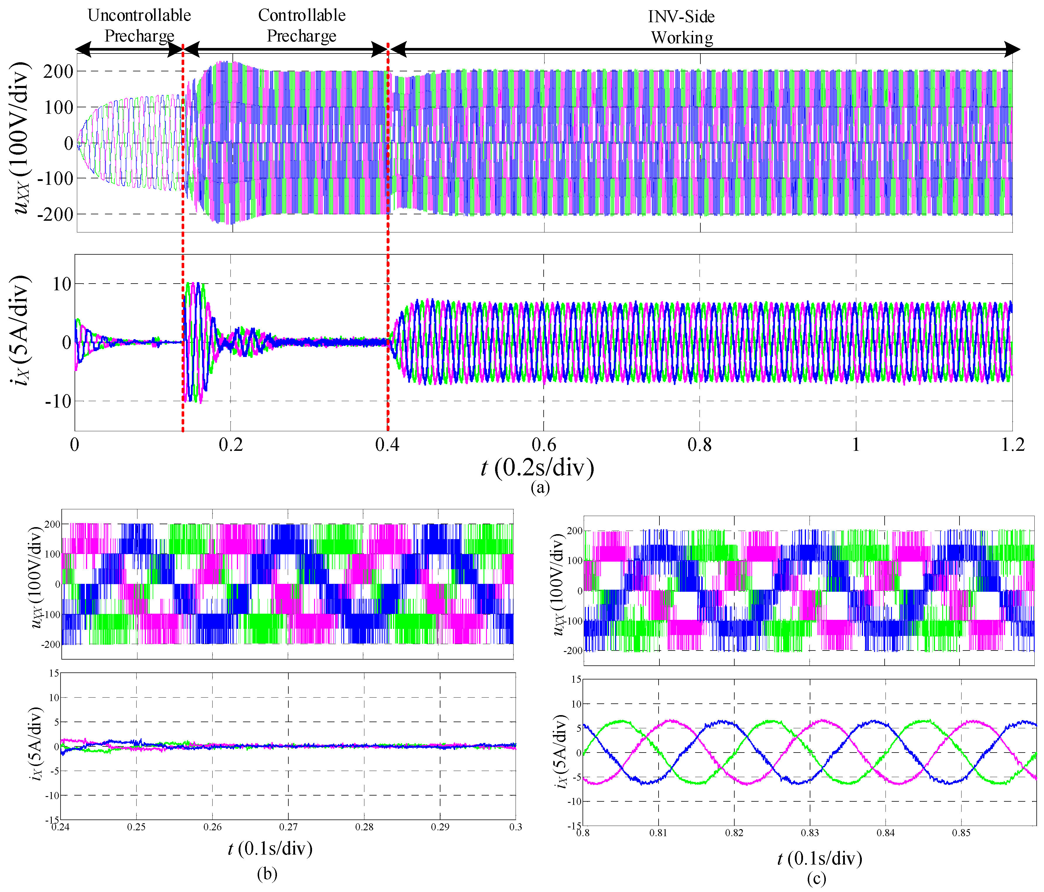
The simulation result is shown in Figure 16. The whole working process shown in Figure 16a, is divided into three sections: uncontrollable precharge, controllable precharge, and inverter side working. In the uncontrollable precharge section, uncontrollable full wave rectification is achieved only by diodes with anti-parallel device. Then the rectifier side starts in Power Unit Ⅱ, and the voltages of modules SMX1 and SMX2 are selected as 50 V and 100 V, respectively. Figure 16b,c shows line-to-line voltages and three-phase currents of the rectifier side under the modulation index set at 1. Obviously, the voltage reaches nine levels and the currents are undistorted sinusoidal waveforms.
5. Conclusions
In order to balance the voltage of flying-capacitors, a novel three-level voltage source converter for AC–DC–AC conversion was proposed in this paper. The circuit configuration and work principle of the proposed three-level voltage source converter were studied in detail. The dual double-closed-loop control strategy and voltage balancing algorithm, especially the method of inverter capacitors with OSSC, were introduced to elaborate the control method of a three-level converter. Then, two operation conditions were analyzed to assess the operating characteristics of the proposed converter. Finally, the balanced control capabilities of this new topology to the three-phase suspension capacitor voltage of the rectifier side and inverter side was verified by simulations and experiments.
Author Contributions
Conceptualization, Z.Y. and X.D.; Methodology, A.C.; Software, S.M.; Validation, A.C., T.W. and S.M.; Formal Analysis, D.Y.; Investigation, T.W.; Resources, Z.Y.; Data Curation, D.Y.; Writing-Original Draft Preparation, A.C.; Writing-Review & Editing, T.W.; Visualization, S.M.; Supervision, S.M.; Project Administration, Z.Y.; Funding Acquisition, X.D.
Funding
This work has been partially supported by the Fundamental Research Funds for the Central Universities under Award 2015XKMS030 and the National Natural Science Foundation of China (U1610113).
Conflicts of Interest
The authors declare no conflict of interest.
References
- Nguyen, L.V.; Tran, H.D.; Johnson, T.T. Virtual prototyping for distributed control of a fault-tolerant modular multilevel inverter for photovoltaics. IEEE Trans. Energy Convers. 2014, 29, 841–850. [Google Scholar] [CrossRef]
- Alishah, R.S.; Hosseini, S.H.; Babaei, E.; Sabahi, M. A New General Multilevel Converter Topology Based on Cascaded Connection of Submultilevel Units With Reduced Switching Components, DC Sources, and Blocked Voltage by Switches. IEEE Trans. Ind. Electron. 2016, 63, 7157–7164. [Google Scholar] [CrossRef]
- Buccella, C.; Cecati, C.; Cimoroni, M.G.; Razi, K. Analytical method for pattern generation in five-level cascaded H-bridge inverter using selective harmonic elimination. IEEE Trans. Ind. Electron. 2014, 61, 5811–5819. [Google Scholar] [CrossRef]
- Zamiri, E.; Vosoughi, N.; Hosseini, S.H.; Barzegarkhoo, R.; Sabahi, M. A New Cascaded Switched-Capacitor Multilevel Inverter Based on Improved Series–Parallel Conversion with Less Number of Components. IEEE Trans. Ind. Electron. 2016, 63, 3582–3594. [Google Scholar] [CrossRef]
- Tolbert, L.M.; Fang, Z.P.; Thomas, G.H. Multilevel Converters for Large Electric Drives. IEEE Trans. Ind. Appl. 1999, 35, 36–44. [Google Scholar] [CrossRef]
- Teymour, H.R.; Sutanto, D.; Muttaqi, K.M. Solar PV and Battery Storage Integration using a New Configuration of a Three-Level NPC Inverter With Advanced Control Strategy. IEEE Trans. Energy Convers. 2014, 29, 354–365. [Google Scholar]
- Pouresmaeil, E.; Montesinos-Miracle, D.; Gomis-Bellmunt, O. Control scheme of three-level NPC inverter for integration of renewable energy resources into AC grid. IEEE Syst. J. 2012, 6, 242–253. [Google Scholar] [CrossRef]
- Peng, F.Z.; Lai, J.S.; McKeever, J.W. A multilevel voltage-source inverter with separate DC sources for static var generation. IEEE Trans. Ind. Appl. 1996, 32, 1130–1138. [Google Scholar] [CrossRef]
- Pou, J.; Ceballos, S.; Knstantinou, G. Circulating current injection methods based on instantaneous information for the modular multilevel converter. IEEE Trans. Ind. Electron. 2015, 62, 777–788. [Google Scholar] [CrossRef]
- Meshram, P.M.; Borghate, V.B. A simplified nearest level control (NLC) voltage balancing method for modular multilevel converter (MMC). IEEE Trans. Power Electron. 2015, 30, 450–462. [Google Scholar] [CrossRef]
- Hatti, N.; Hasegawa, K.; Akagi, H. A 6.6-kV transformerless motor drive using a five-level diode-clamped PWM inverter for energy savings of pumps and blowers. IEEE Trans. Power Electron. 2009, 24, 796–803. [Google Scholar] [CrossRef]
- Ghias, A.M.Y.M.; Pou, J.; Agelidis, V.G.; Ciobotaru, M. Optimal switching transition-based voltage balancing method for flying capacitor multilevel converters. IEEE Trans. Power Electron. 2015, 30, 1804–1817. [Google Scholar] [CrossRef]
- Oikonomou, N.; Gutscher, C.; Karamanakos, P.; Kieferndorfand, F.D.; Geyer, T. Model predictive pulse pattern control for the five-level active neutral-point-clamped inverter. IEEE Trans. Ind. Appl. 2013, 49, 2583–2592. [Google Scholar] [CrossRef]
- Roshankumar, P.; Rajeevan, P.P.; Mathew, K.; Leon, J.I.; Franquelo, L.G. A five-level inverter topology with single-DC supply by cascading a flying capacitor inverter and an H-bridge. IEEE Trans. Power Electron. 2012, 27, 3505–3512. [Google Scholar] [CrossRef]
- Ooi, G.H.P.; Maswood, A.L.; Lim, Z. Five-level multiple-pole PWM AC-AC converters with reduced components count. IEEE Trans. Ind. Electron. 2015, 62, 4739–4748. [Google Scholar] [CrossRef]
- Narimani, M.; Wu, B.; Cheng, Z.; Zargari, N.R. A new nested neutral point-clamped (NNPC) converter for medium-voltage (MV) power conversion. IEEE Trans. Power Electron. 2014, 29, 6375–6382. [Google Scholar] [CrossRef]
- Cortes, P.; Wilson, A.; Kouro, S.; Rodriguez, J.; Abu-Rub, H. Model predictive control of multilevel cascaded H-bridge inverters. IEEE Trans. Ind. Electron. 2010, 57, 2691–2699. [Google Scholar] [CrossRef]
- Kouro, S.; Malinowski, M.; Gopakumar, K.; Pou, J.; Franquelo, L.G.; Wu, B.; Rodriguez, J.; Perez, M.A.; Leon, J.I. Recent Advances and Industrial Applications of Multilevel Converters. IEEE Trans. Ind. Electron. 2010, 57, 2553–2580. [Google Scholar] [CrossRef]
- Veenstra, M.; Rufer, A. Hybrid Cascaded Control of a Hybrid Asymmetric Multilevel Inverter for Competitive Medium-Voltage Industrial Drives. IEEE Trans. Ind. Appl. 2005, 41, 655–664. [Google Scholar] [CrossRef]
- Venugopal, J.; Subarnan, G.M. Hybrid cascaded MLI topology using ternary voltage progression technique with multicarrier strategy. J. Electr. Eng. Technol. 2015, 10, 1610–1620. [Google Scholar] [CrossRef]
- Miranbeigi, M.; Iman-Eini, H.; Asoodar, M. A new switching strategy for transformer-less back-to-back cascaded H-bridge multilevel converter. IET Power Electron. 2014, 7, 1868–1877. [Google Scholar] [CrossRef]
- Kongnun, W.; Sangswang, A.; Chotigo, S. Design of a cascaded H-bridge converter for insulation testing. In Proceedings of the IEEE International Symposium on Industrial Electronics, Seoul, Korea, 5–8 July 2009; pp. 859–863. [Google Scholar]
- Blahnik, V.; Peroutka, Z.; Talla, J. Control of cascaded H-bridge active rectifier providing active voltage balancing. In Proceedings of the 40th Annual Conference of the IEEE Industrial Electronics Society, IECON 2014, Dallas, TX, USA, October–1 November 2015; pp. 4589–4594. [Google Scholar]
- Islam, M.R.; Guo, Y.; Zhu, J.G. Performance and cost Comparison of NPC, FC and SCHB Multilevel Converter Topologies for High-voltage Applications. In Proceedings of the International Conference on Electrical Machines and Systems, Beijing, China, 20–23 August 2011; pp. 1–6. [Google Scholar]
- Fazel, S.S.; Bernet, S.; Krug, D.; Jalili, K. Design and Comparison of 4-kv Neutral-point-clamped, Flying-capacitor, and Series-connected H-bridge Multilevel Converters. IEEE Tran. Ind. Appl. 2007, 43, 1032–1040. [Google Scholar] [CrossRef]
- Minambres-Marcos, V.; Guerrero-Martinez, M.A.; Romero-Cadaval, E.; Milanes-Montero, M.I. Generic Losses Model for Traditional Inverters and Neutral Point Clamped Inverters. Electron. Electr. Eng. 2014, 20, 84–88. [Google Scholar] [CrossRef]
- Ye, Z.B.; Xu, Y.M.; Li, F.; Deng, X.M.; Zhang, Y.Z. Simplified PWM Strategy for Neutral-Point-Clamped (NPC) Three-Level Converter. J. Power Electron. 2014, 14, 519–530. [Google Scholar] [CrossRef]
Figure 1.
Circuit configuration of the proposed three-level voltage source converter.
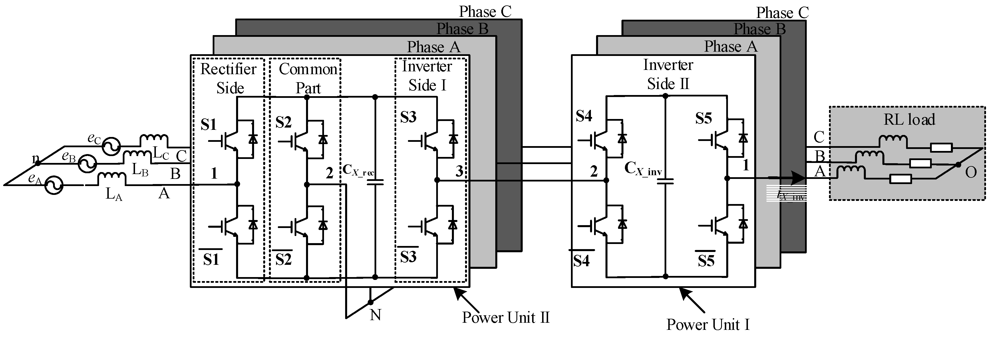
Figure 2.
Switching losses comparison.
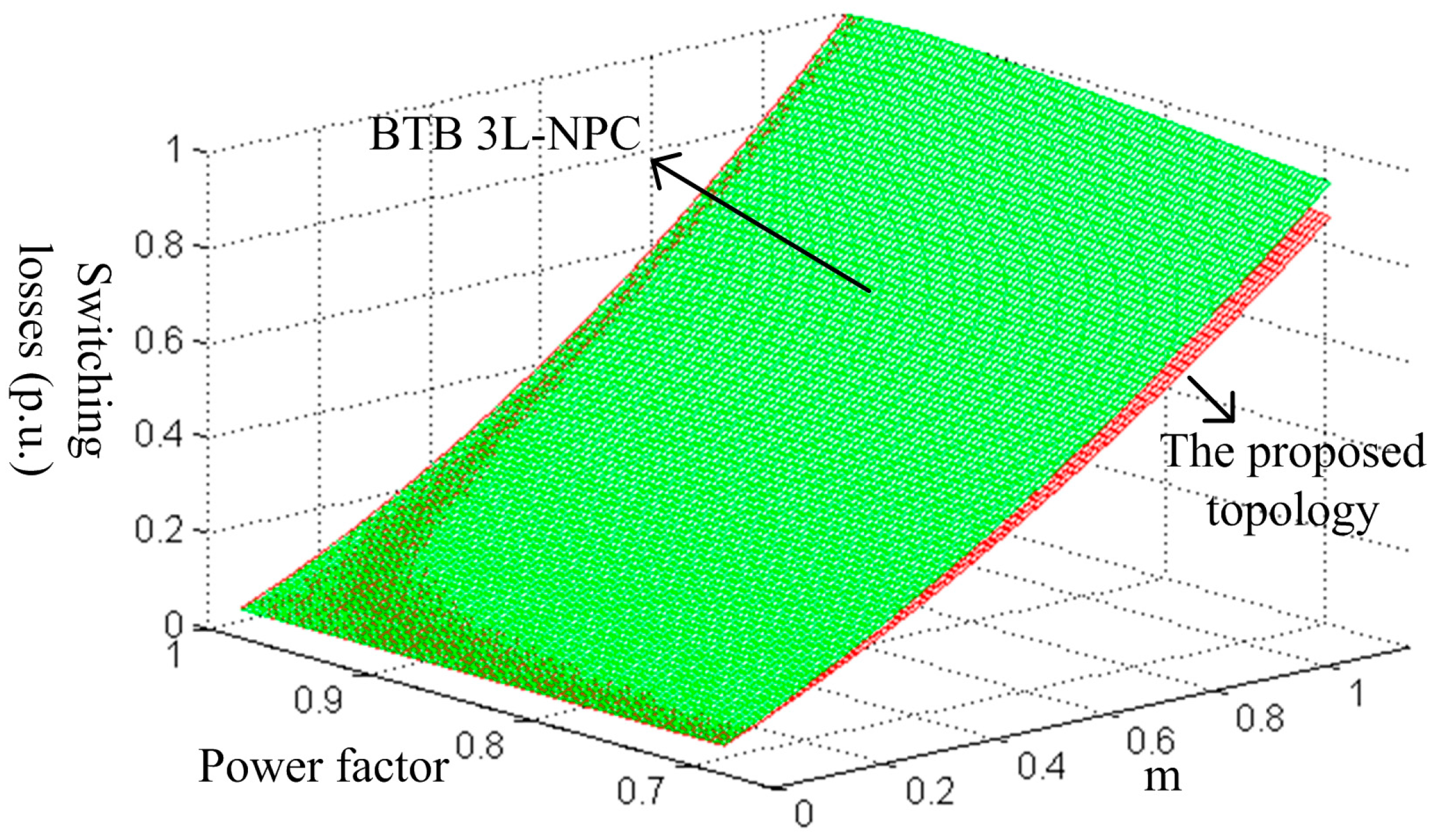
Figure 3.
Control block diagram of the proposed multilevel converter.
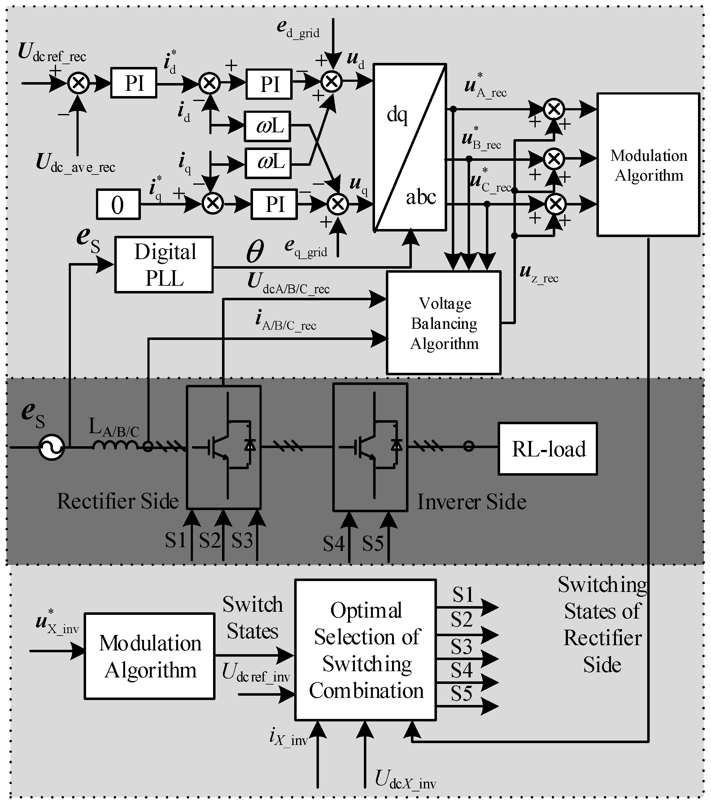
Figure 4.
Sectors for the proposed three-level converter with the simplified PWM.
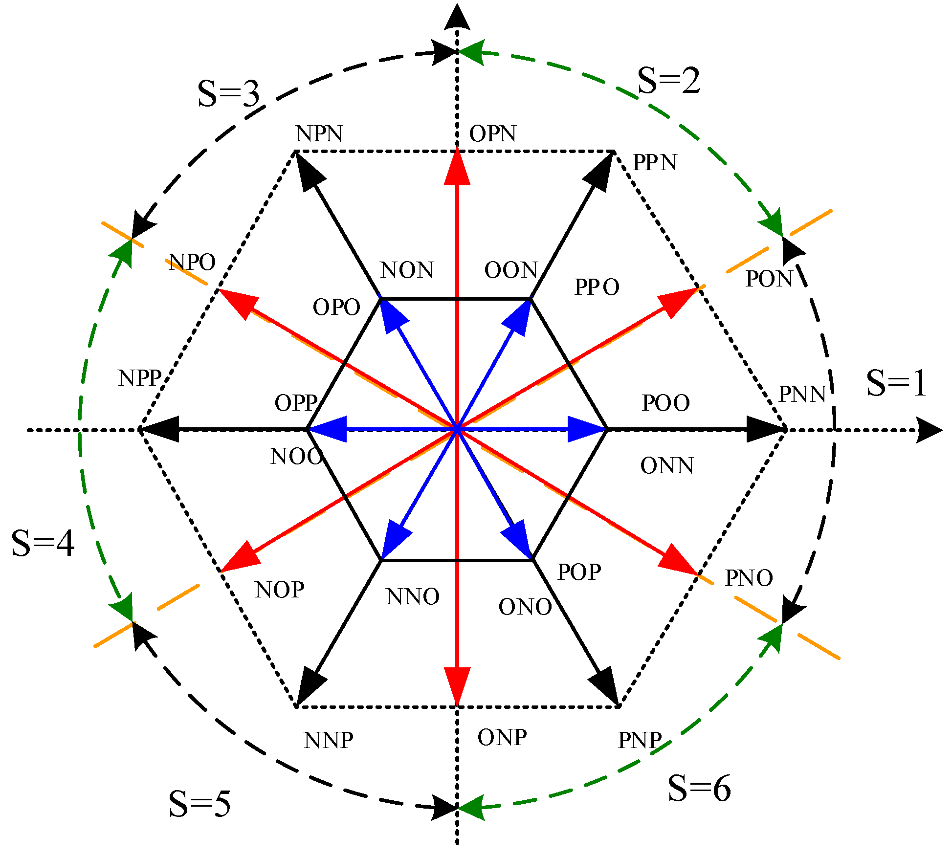
Figure 5.
Current paths of S1S2 when iX_rec > 0 and (u*X_rec − uz_rec) > 0.
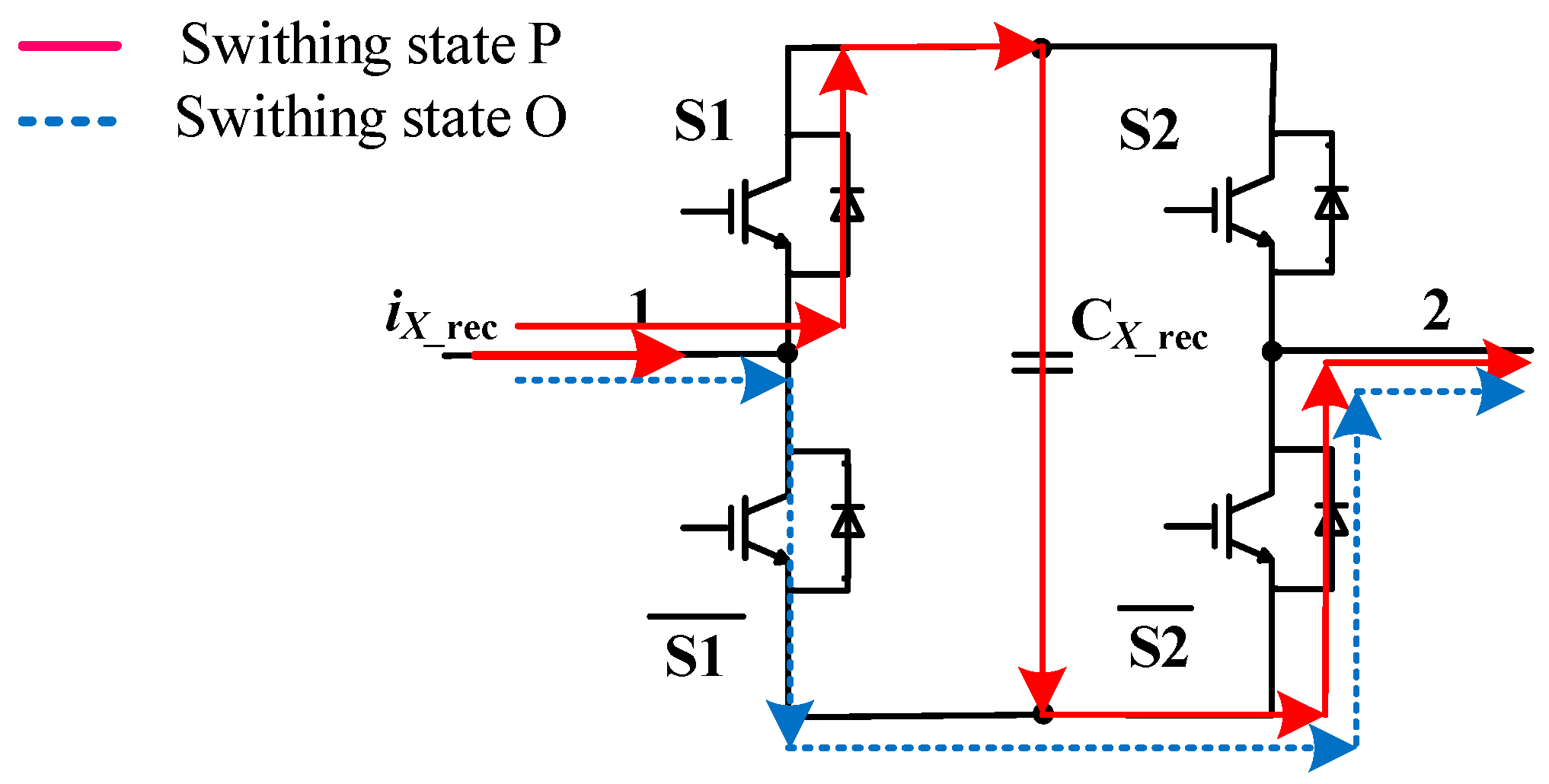
Figure 6.
Voltage balancing algorithm of CX_rec.

Figure 7.
The discharging and keeping paths of capacitor CX_inv.

Figure 8.
Converter state and switching commands. (a) (u*A_rec − uz_rec) < 0, (u*A_inv − uz) > 0, and UdcA_inv > Udcref_inv; iX_inv > 0, TA_rec > TA_inv; (b) (u*A_rec − uz_rec) < 0, (u*A_inv − uz) > 0, and UdcA_inv > Udcref_inv; iX_inv < 0, TA_rec < TA_inv.
Figure 8.
Converter state and switching commands. (a) (u*A_rec − uz_rec) < 0, (u*A_inv − uz) > 0, and UdcA_inv > Udcref_inv; iX_inv > 0, TA_rec > TA_inv; (b) (u*A_rec − uz_rec) < 0, (u*A_inv − uz) > 0, and UdcA_inv > Udcref_inv; iX_inv < 0, TA_rec < TA_inv.

Figure 9.
Analysis of voltage deviation with CA_inv. (a) When Sgn|(u*A_rec − uz_rec)| = −Sgn|(u*A_inv − uz)|; (b) when minv < 1 − mrec.
Figure 9.
Analysis of voltage deviation with CA_inv. (a) When Sgn|(u*A_rec − uz_rec)| = −Sgn|(u*A_inv − uz)|; (b) when minv < 1 − mrec.
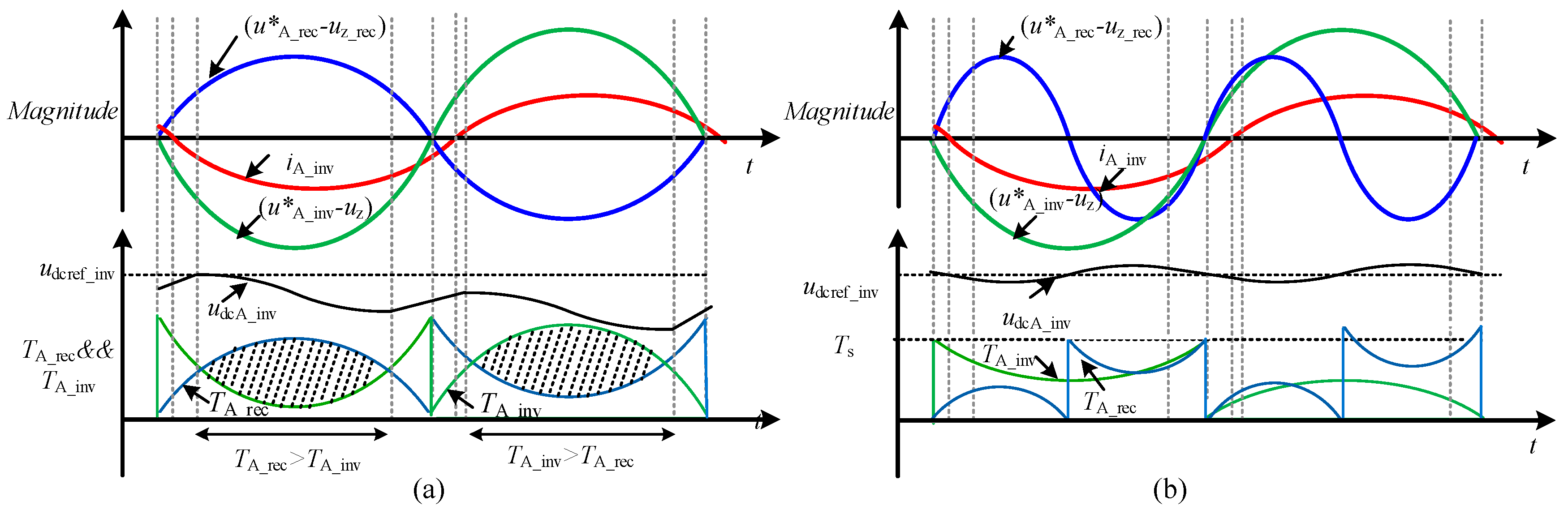
Figure 10.
Experimental setup for the proposed multilevel converter.
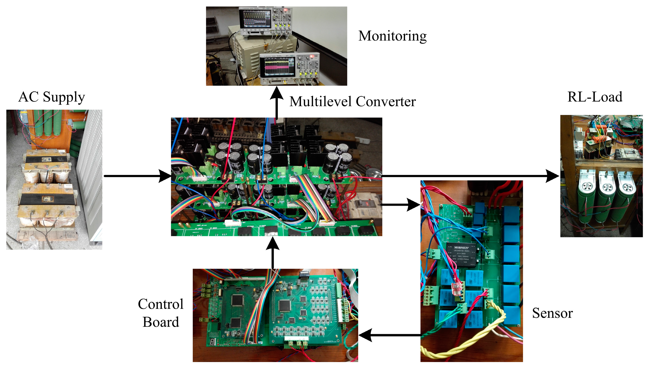
Figure 11.
Experimental results of the whole working-process in transient-state condition; (a) Input voltage–current waveforms, eA_rec and iX_rec; (b) voltages of CX_rec; (c) output voltage–current waveforms, uAB_inv and iX_inv; (d) voltages of CX_inv.
Figure 11.
Experimental results of the whole working-process in transient-state condition; (a) Input voltage–current waveforms, eA_rec and iX_rec; (b) voltages of CX_rec; (c) output voltage–current waveforms, uAB_inv and iX_inv; (d) voltages of CX_inv.

Figure 12.
Experimental results of the whole working process in transient-state conditions; (a) Input voltage–current waveforms, eA_rec and iX_rec; (b) voltages of CX_rec; (c) output voltage–current waveforms, uAB_inv and iX_inv; (d) voltages of CX_inv.
Figure 12.
Experimental results of the whole working process in transient-state conditions; (a) Input voltage–current waveforms, eA_rec and iX_rec; (b) voltages of CX_rec; (c) output voltage–current waveforms, uAB_inv and iX_inv; (d) voltages of CX_inv.
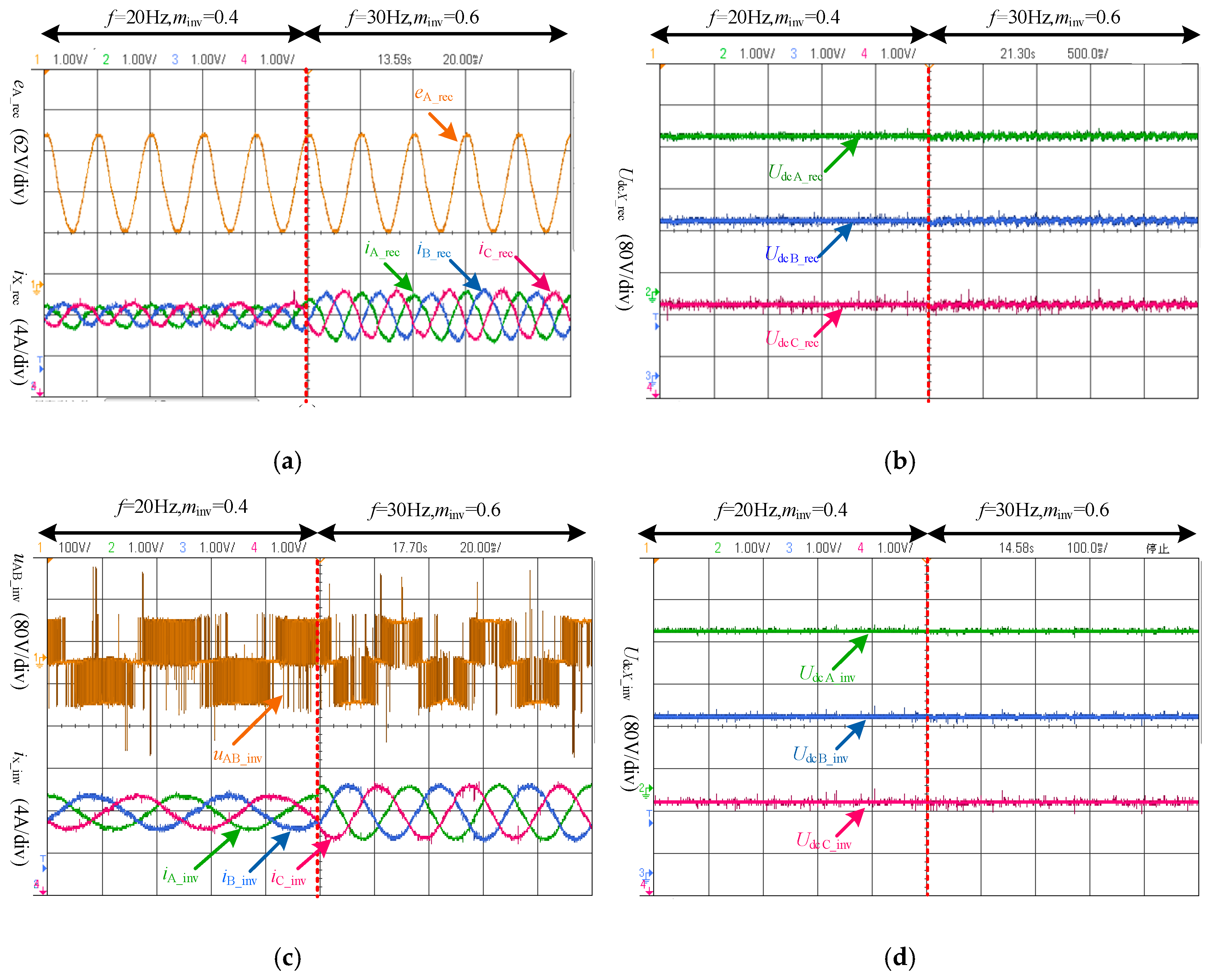
Figure 13.
Experimental results of the multilevel converter in transient-state conditions; minv changes from 0.8 to 0.9; (a) Input voltage-current waveforms, eA_rec and iX_rec; (b) voltages of CX_rec; (c) output voltage–current waveforms, uAB_inv and iX_inv; (d) voltages of CX_inv.
Figure 13.
Experimental results of the multilevel converter in transient-state conditions; minv changes from 0.8 to 0.9; (a) Input voltage-current waveforms, eA_rec and iX_rec; (b) voltages of CX_rec; (c) output voltage–current waveforms, uAB_inv and iX_inv; (d) voltages of CX_inv.

Figure 14.
Harmonic characteristic results of WTHD curves of uAB_inv with fswitch and minv.
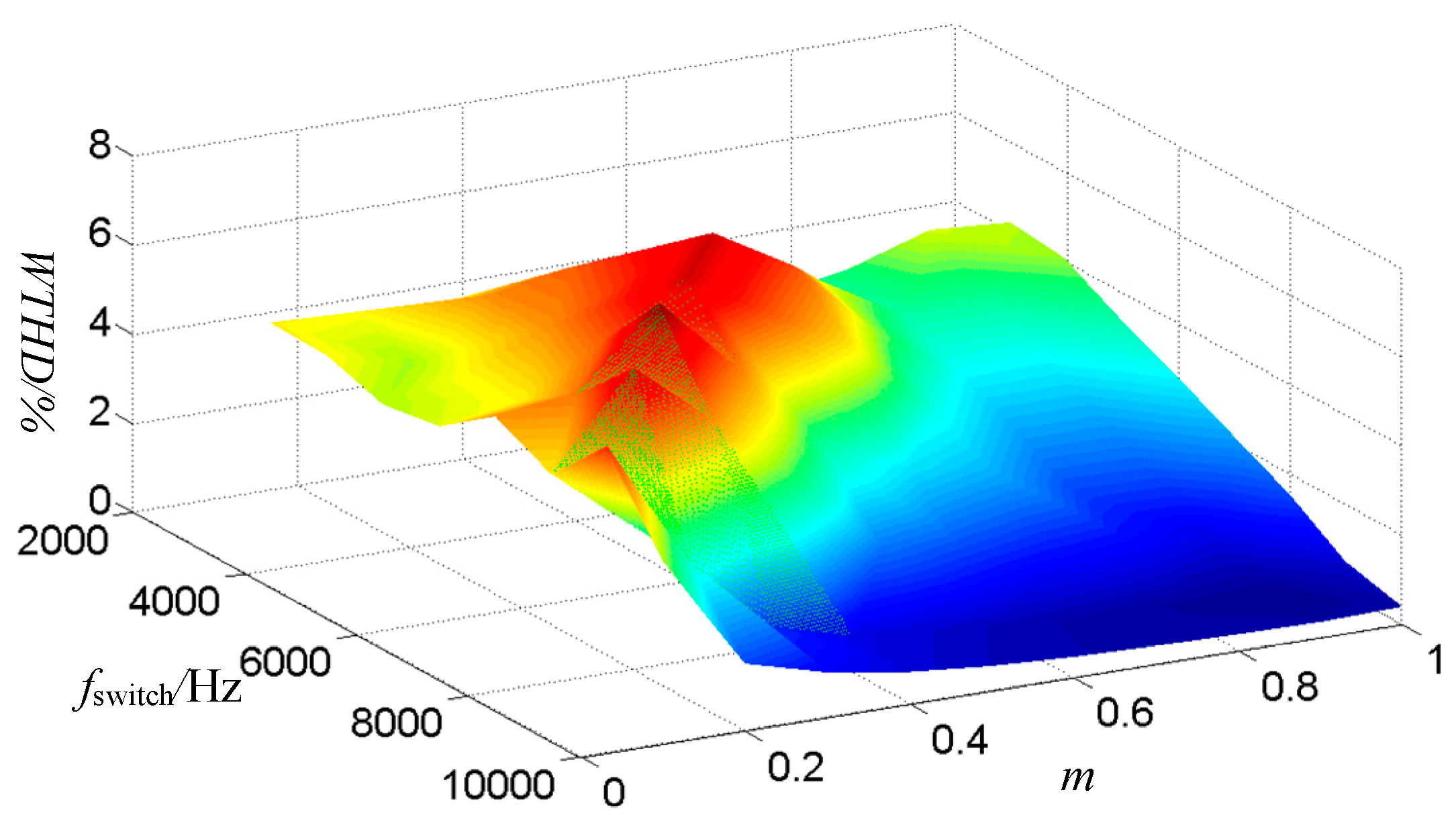
Figure 15.
Circuit configuration of 5/3 level voltage source converter.
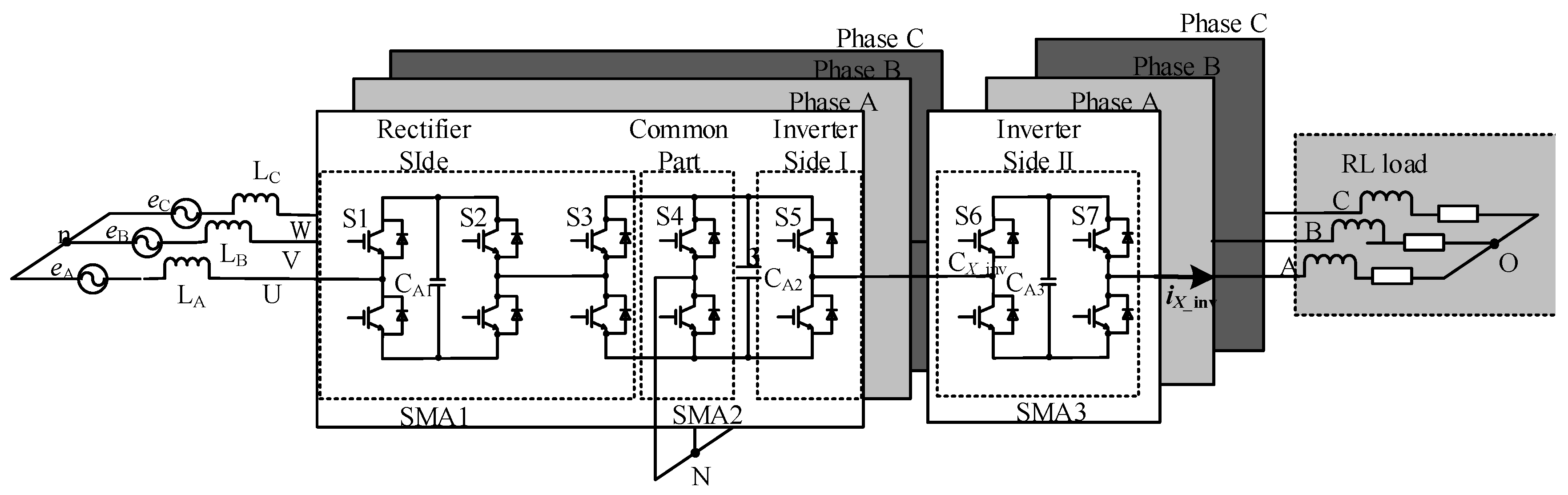
Figure 16.
Simulation results of the whole working process; (a) Output voltage–current waveforms, uxx and iX; (b) Output voltage–current waveforms, uxx and iX ; time from 0.24s to 0.3s;(c) Output voltage–current waveforms, uxx and iX; time from 0.8 s to 0.86 s.
Figure 16.
Simulation results of the whole working process; (a) Output voltage–current waveforms, uxx and iX; (b) Output voltage–current waveforms, uxx and iX ; time from 0.24s to 0.3s;(c) Output voltage–current waveforms, uxx and iX; time from 0.8 s to 0.86 s.

Table 1.
Switching states of rectifier side and inverter side.
| Rectifier State | S1 S2 | Inverter State | S3 S4 S5 |
|---|---|---|---|
| P | S1S2 = 10 | P | S3 = 1, S4 = S5 or S3 = 0, S4 = 0, S5 = 1 |
| O | S3 = 0, S4 = S5 or S3 = 1, S4 = 1, S5 = 0 | ||
| N | S3 = 0, S4 = 1, S5 = 0 | ||
| O | S1 = S2 | P | S3 = S2, S4 = 0, S5 = 1 or S2 = 0, S3 = 1, S4 = S5 |
| O | S2 = S3, S4 = S5 or S2 = 1, S3 = 0,S4 = 0, S5 = 1 or S2 = 0, S3 = 1, S4 = 1, S5 = 0 | ||
| N | S2 = S3, S4 = 1, S5 = 0 or S2 = 1, S3 = 0, S4 = S5 | ||
| N | S1S2 = 01 | P | S3 = 1, S4 = 0, S5 = 1 |
| O | S3 = 1, S4 = S5 or S3 = 0, S4 = 0, S5 = 1 | ||
| N | S3 = 1, S4 = 1, S5 = 0 or S3 = 0, S4 = S5 |
Table 2.
Comparison of different topologies (Vll_rms = 3 kV, Iph_rms = 115.5 A, P = 600 kW).
| Level | 3L | 5L | ||||||
|---|---|---|---|---|---|---|---|---|
| Topology | NPC | FC | CHB | CMC | NPC | FC | CHB | CMC |
| Rated device voltage (IGBT) | 4.5 kV | 4.5 kV | 4.5 kV | 4.5 kV | 3.3 kV | 3.3 kV | 3.3 kV | 3.3 kV |
| Rated device current (IGBT) | 450 A | 450 A | 450 A | 450 A | 450 A | 450 A | 450 A | 450 A |
| IGBTs | 24 | 24 | 24 | 30 | 48 | 48 | 48 | 54 |
| Diodes | 12 | --- | --- | --- | 36 | --- | --- | --- |
| Capacitors | 2 + 0 | 2 + 6 | 3 + 0 | 6 + 0 | 4 + 0 | 4 + 18 | 6 + 0 | 12 + 0 |
| Total Components | 38 | 32 | 23 | 36 | 88 | 70 | 54 | 66 |
Table 3.
Value of .
| a1 | a2 | utemp1, utemp2 | uz_rec |
|---|---|---|---|
| >0 | >0 | utemp1 > utemp2 | utemp1 |
| utemp1 ≤ utemp2 | utemp2 | ||
| <0 | utemp1 > utemp2 | 0 | |
| utemp1 ≤ utemp2 | (utemp1 + utemp2)/2 | ||
| <0 | >0 | utemp1 > utemp2 | (utemp1 + utemp2)/2 |
| utemp1 ≤ utemp2 | 0 | ||
| <0 | utemp1 > utemp2 | utemp2 | |
| utemp1 ≤ utemp2 | utemp1 |
Table 4.
Switching states of rectifier side and inverter side.
| Inverter State | iX_inv | S2 | Inverter Side I | Inverter Side II | Switch Combinations | Charge State |
|---|---|---|---|---|---|---|
| P | >0 | 1 | O | P | S3S4S5 = 101 | D |
| 0 | O | P | S3S4S5 = 001 | D | ||
| P | O | S3 = 1, S4 = S5 | K | |||
| ≤0 | 1 | O | P | S3S4S5 = 101 | C | |
| 0 | P | O | S3 = 1, S4 = S5 | K | ||
| O | P | S3S4S5 = 001 | C | |||
| O | >0 | 1 | N | P | S3S4S5 = 001 | D |
| O | O | S3 = 1, S4 = S5 | K | |||
| 0 | O | O | S3 = 0, S4 = S5 | K | ||
| P | N | S3S4S5 = 110 | C | |||
| ≤0 | 1 | O | O | S3 = 1, S4 = S5 | K | |
| N | P | S3S4S5 = 001 | C | |||
| 0 | P | N | S3S4S5 = 110 | D | ||
| O | O | S3 = 0, S4 = S5 | K | |||
| N | >0 | 1 | N | O | S3 = 0, S4 = S5 | K |
| O | N | S3S4S5 = 110 | C | |||
| 0 | O | N | S3S4S5 = 010 | C | ||
| 1 | O | N | S3S4S5 = 110 | D | ||
| N | O | S3 = 0, S4 = S5 | K | |||
| 0 | O | N | S3S4S5 = 010 | D |
C: Charging; D: Discharge; K: Keeping.
Table 5.
Switching states of rectifier side and inverter side.
| u*A_rec − uz_rec | u*A_inv − uz | UdcA_inv | iA_inv | tS1 | tS2 | tS3 | tS4 | tS5 |
|---|---|---|---|---|---|---|---|---|
| >0 | >0 | UdcA_inv > Udcref_inv | >0 | TA_rec | 0 | 0 | 0 | TA_inv |
| ≤0 | TA_rec | 0 | Ts | Ts | TA_inv | |||
| UdcA_inv ≤ Udcref_inv | >0 | |||||||
| ≤0 | TA_rec | 0 | 0 | 0 | TA_inv | |||
| ≤0 | UdcA_inv > Udcref_inv | >0 | Ts | TA_rec | 0 | TA_rec | TA_inv | |
| ≤0 | TA_rec | 0 | TA_inv | Ts | 0 | |||
| UdcA_inv ≤ Udcref_inv | >0 | |||||||
| ≤0 | Ts | TA_rec | 0 | TA_rec | TA_inv | |||
| ≤0 | >0 | UdcA_inv > Udcref_inv | >0 | TA_rec | Ts | TA_inv | 0 | Ts |
| ≤0 | 0 | TA_rec | Ts | TA_rec | TA_inv | |||
| UdcA_inv ≤ Udcref_inv | >0 | |||||||
| ≤0 | TA_rec | Ts | TA_inv | 0 | Ts | |||
| ≤0 | UdcA_inv > Udcref_inv | >0 | TA_rec | Ts | 0 | 0 | TA_inv | |
| ≤0 | TA_rec | Ts | Ts | Ts | TA_inv | |||
| UdcA_inv ≤ Udcref_inv | >0 | |||||||
| ≤0 | TA_rec | Ts | 0 | 0 | TA_inv |
tS1~S5 is the duration time of each switch, S1~S5.
Table 6.
Parameter settings for simulation and experiment.
| Parameter | Value |
|---|---|
| Source voltage, eX_rec | 55 V |
| DC-link voltage | 100 V |
| DC-link capacitor | 1200 μF |
| Filter-inductive | 2.2 mH |
| Resistive-inductive load | 20 Ω, 2.2 mH |
| Switching frequency | 5 kHz |
© 2018 by the authors. Licensee MDPI, Basel, Switzerland. This article is an open access article distributed under the terms and conditions of the Creative Commons Attribution (CC BY) license (http://creativecommons.org/licenses/by/4.0/).
Share and Cite
MDPI and ACS Style
Ye, Z.; Chen, A.; Mao, S.; Wang, T.; Yu, D.; Deng, X. A Novel Three-Level Voltage Source Converter for AC–DC–AC Conversion. Energies 2018, 11, 1147. https://doi.org/10.3390/en11051147
AMA Style
Ye Z, Chen A, Mao S, Wang T, Yu D, Deng X. A Novel Three-Level Voltage Source Converter for AC–DC–AC Conversion. Energies. 2018; 11(5):1147. https://doi.org/10.3390/en11051147
Chicago/Turabian StyleYe, Zongbin, Anni Chen, Shiqi Mao, Tingting Wang, Dongsheng Yu, and Xianming Deng. 2018. "A Novel Three-Level Voltage Source Converter for AC–DC–AC Conversion" Energies 11, no. 5: 1147. https://doi.org/10.3390/en11051147
Note that from the first issue of 2016, this journal uses article numbers instead of page numbers. See further details here.