An Overview of Regulation Topologies in Resonant Wireless Power Transfer Systems for Consumer Electronics or Bio-Implants


School of Electronics and Information Engineering, South China University of Technology, Wushan, Guangzhou 510641, China
*
Author to whom correspondence should be addressed.
Energies 2018, 11(7), 1737; https://doi.org/10.3390/en11071737
Submission received: 31 May 2018
/
Revised: 18 June 2018
/
Accepted: 25 June 2018
/
Published: 3 July 2018
(This article belongs to the Special Issue Wireless Power Transfer 2018)
Abstract
:Owing to its relatively high efficiency, extended transmission range, and less exposure to radio frequency radiation, near-field resonant wireless power transfer (R-WPT) has been widely used in consumer electronics and bio-implants. For most applications, a well-regulated output voltage is required against the coupling and loading variations, and thus a regulation scheme should be employed in an R-WPT system. To achieve an optimal receiver (RX) or overall efficiency, together with a reduced cost overhead, several regulation schemes have been proposed in recent years, where the regulation can be implemented at either the RX or transmitter (TX) side, or both. These regulation schemes have been reviewed and comprehensively discussed in this paper. Hence, the main contribution of this paper is to provide a guideline for designing the regulation scheme in R-WPT systems. Moreover, potential new topologies of regulation are investigated here.
1. Introduction
The wireless power transfer (WPT) technique is at the critical point of explosive growth. Many consumer electronics and bio-implant systems have integrated WPT circuits for their compactness, being water-proof, and their reduced maintenance cost. However, the WPT circuits’ transfer efficiency is inherently lower than that of their wired counterparts [1,2]. To balance this trade-off, high-efficiency WPT techniques, e.g., near-field transmission (such as inductive, resonant, capacitive, and ultrasonic power transfer), may be more favorable than far-field WPT (such as optical and microwave). In addition, the near-field technique advances far-field WPT in terms of less exposure to radio frequency (RF) radiation. Among the near-field WPT techniques, resonant WPT (R-WPT) has gradually drawn widespread attention. This is because the R-WPT technique can extend the power transfer range to several tens of centimeters, which is much wider than that of the inductive coupling technique. On one other hand, the resonant coupling technique does not require a precise coil alignment and tight coupling, and thus multiple receivers can be applied to receive power from a transmitter.
Some previous studies have reviewed the R-WPT techniques [3,4,5,6,7]. In [3,4], the historical background, challenges, and engineering applications of R-WPT were discussed. The authors in [5] presented the coil design challenges. A comparison between the inductive and capacitive power transfer in power level, gap distance, operating frequency, and efficiency were given in [6]. In addition, [7] discussed the design of resonant circuits and the compensation networks for near-field WPT systems.
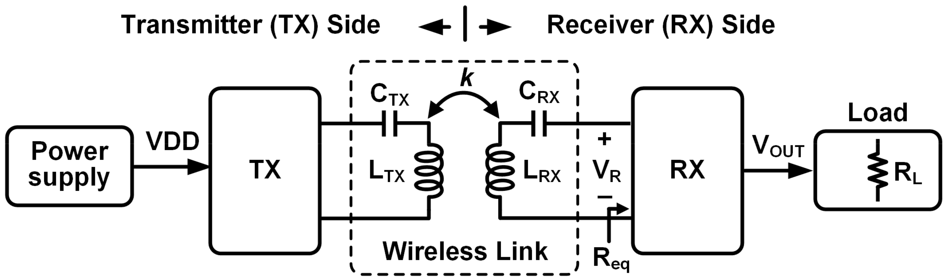
Taking an R-WPT system with series-resonant inductor and capacitor (LC) tanks as an example, as illustrated in Figure 1, it consists of a transmitter (TX), a wireless link, and a receiver (RX). In general, the TX is composed of a direct current (DC)-DC converter for power supply, gate drivers, and a power amplifier (PA), where the VDD is the supply voltage; the wireless link consists of two series LC tanks (LTX CTX and LRX CRX) resonant in the same angular frequency ωres, where k is the coupling coefficient between LTX and LRX; and the RX is composed of a rectifier. The alternating current (AC) power, generated from the PA, is transferred from the LTX to the LRX, where the AC voltage across the LRX is VR and the equivalent resistance seen from the RX is Req. Then, the rectifier converts the VR into a DC voltage VOUT for a given load RL.
There are four important parameters for this WPT system: (1) the power delivered to the load (PDL) equaling to
/RL; (2) the power transmission efficiency (PTE) PDL/PS, where PS is the TX input power; (3) the power conversion efficiency (PCE) PDL/PR, where PR is the RX input power; and (4) the voltage conversion efficiency (VCE) VOUT/VR.
For most of the applications, the power supply should be well-regulated. For instance, the power supply should be regulated to >10 V for the neural stimulators in implantable medical devices (IMDs) [8] or flash memory circuits [9]. For battery charging, a constant current and voltage control is required [10]. Also, the regulation becomes especially important in an R-WPT system considering load and coupling distance variation and a coil misalignment [11]. Additionally, a poorly designed regulation scheme may degrade the PTE. Therefore, a comprehensive review of regulation in R-WPT is essential.
How can the regulation be implemented in an R-WPT system? It is straightforward to fulfill the regulation at the RX side, but it can also be fulfilled at the TX side. For clarification, a simplified circuit model of an R-WPT system is presented in Figure 2a without considering the coil resistance. The PA output can be modeled as a source VPA with a source resistor RS. As shown in Figure 2b, the effect of the RX’s resonant magnetic coupling with the TX is presented as a reflected resistance Rrefl in series with the LTX, which can be written by
where Qload is the loaded Q-factor of the RX resonant tank, which is given by:
It should be noted that the power received by the RX is equivalent to that which dissipates on Rrefl, which can be expressed as
where Vrefl is the voltage across Rrefl. Based on Equation (3), once Vrefl or ITX is regulated at the TX side, the received power can be regulated as well as VOUT. Therefore, regulation can be achieved at the TX side.
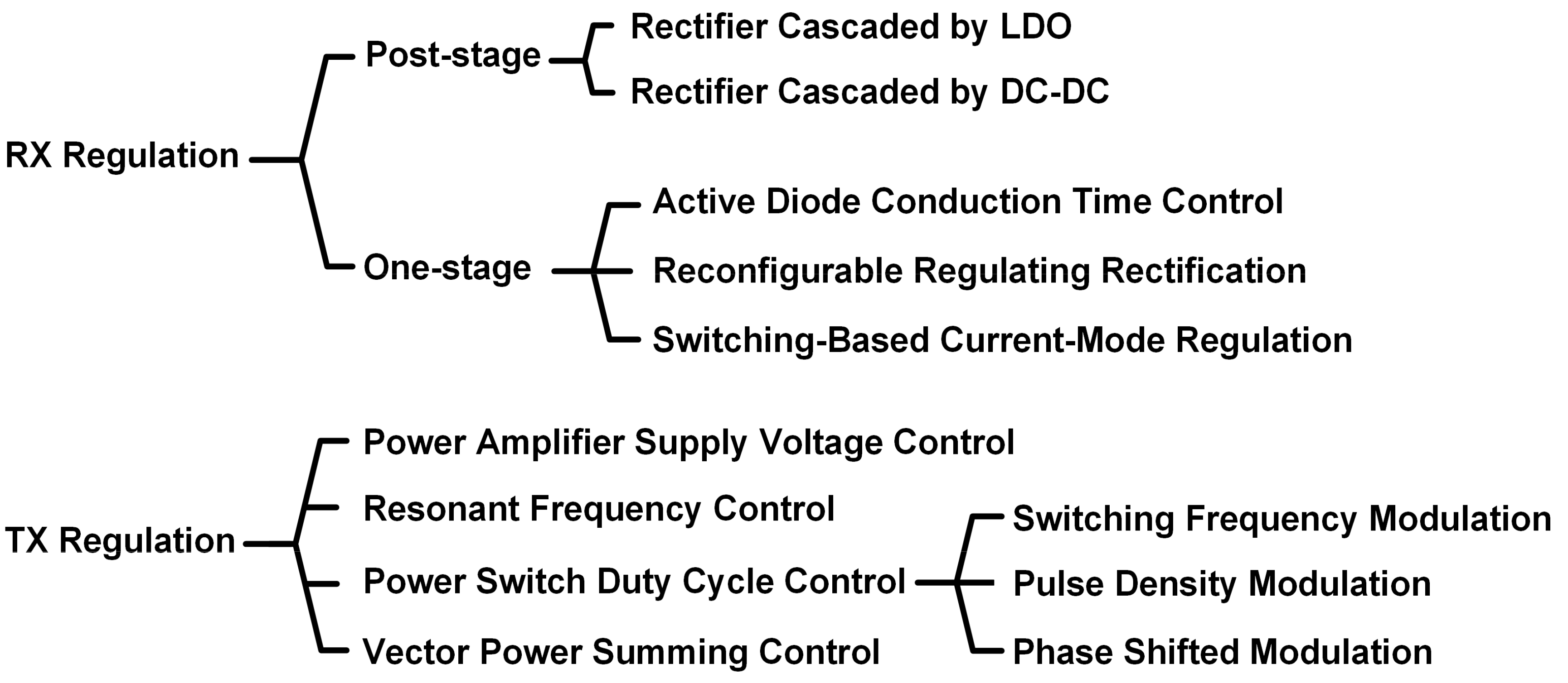
Therefore, the regulation schemes investigated in the previous works can also be categorized into two types: RX and TX regulation. As illustrated in Figure 3, RX regulation includes post-stage regulation (achieved by a cascading low dropout regulator (LDO [12,13,14,15] or a DC–DC converter [16,17,18,19,20]) and one-stage regulation, including active diode conduction time control [21,22,23], reconfigurable regulating rectification [24,25,26,27], and switching-based current-mode regulation [28,29,30,31]. On the other hand, TX regulation can be achieved by PA supply voltage control [32,33], resonant frequency control [34], PA power switch duty cycle control [35,36,37,38,39,40], and vector power summing control [41,42]. Additionally, switching frequency modulation [35,36], pulse density modulation [37,38], and phase-shifted modulation [39,40] can be classified as power switch duty cycle control.
This paper is organized as follows: Section 2 reviews the operation principles of the previous RX regulation topologies. Then, the operation principles of TX regulation are reviewed in Section 3. Possible combinations and potential new topologies are given in Section 4. Finally, a conclusion is drawn in Section 5.
2. RX Regulation
2.1. Post-Stage Regulation
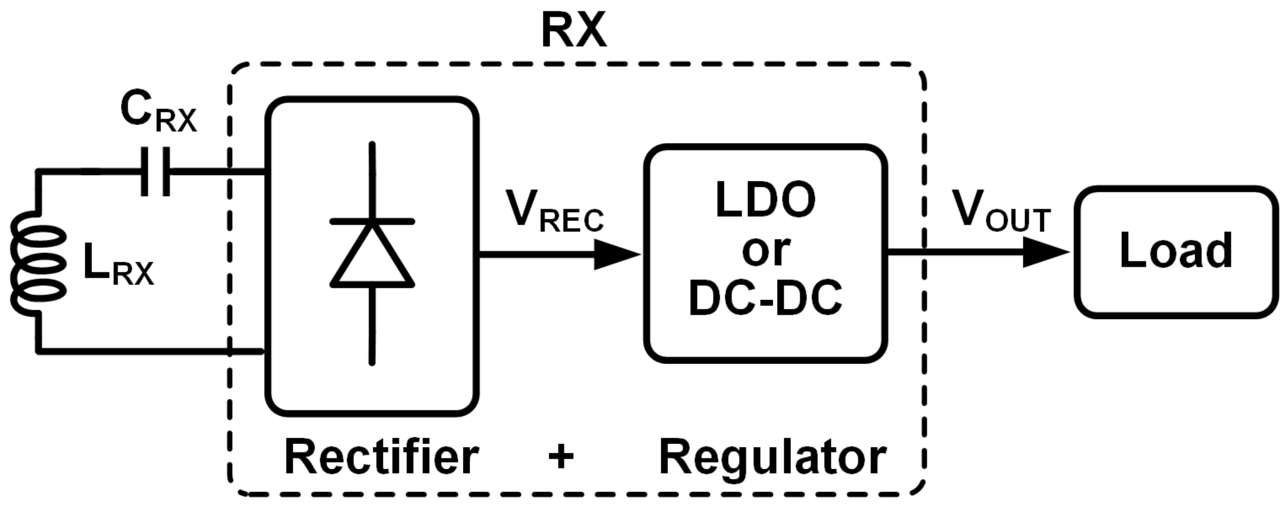
At the RX side, post-stage regulation is straightforward and has been widely used [12,13,14,15,16,17,18,19,20]. This scheme adopts a rectifier cascaded by a regulating stage as shown in Figure 4. Both the LDO [12,13,14,15] and the DC–DC converter [16,17,18,19,20] can be implemented as the cascaded stage. These schemes are discussed as follows.
2.1.1. The Rectifier Cascaded by an LDO
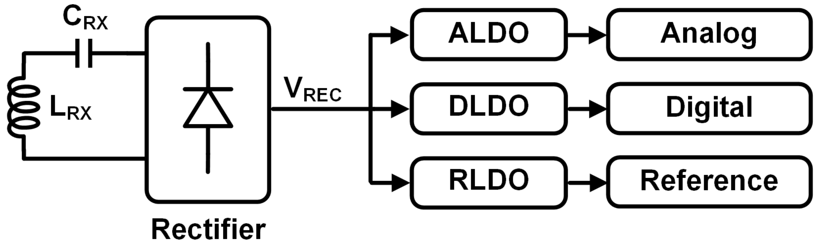
An LDO cascading the rectifier can provide precise regulation while keeping a small voltage ripple compared to a DC–DC converter. For example, as in Figure 5, three LDOs are cascading the rectifier in [12], supplying the analog, digital, and reference circuits, respectively, in a system-on-a-chip (SoC). Additionally, due to the high isolation among LDOs, each regulation loop can be independently optimized. However, the PCE is inherently low due to the LDOs’ efficiency being directly determined by the ratio of the output and input voltages. Therefore, the maximum rectifier efficiency and PCE of [12] was 85% and 74.8%, respectively, which is limited by the efficiency of the post-regulation stage.
2.1.2. The Rectifier Cascaded by a DC–DC Converter
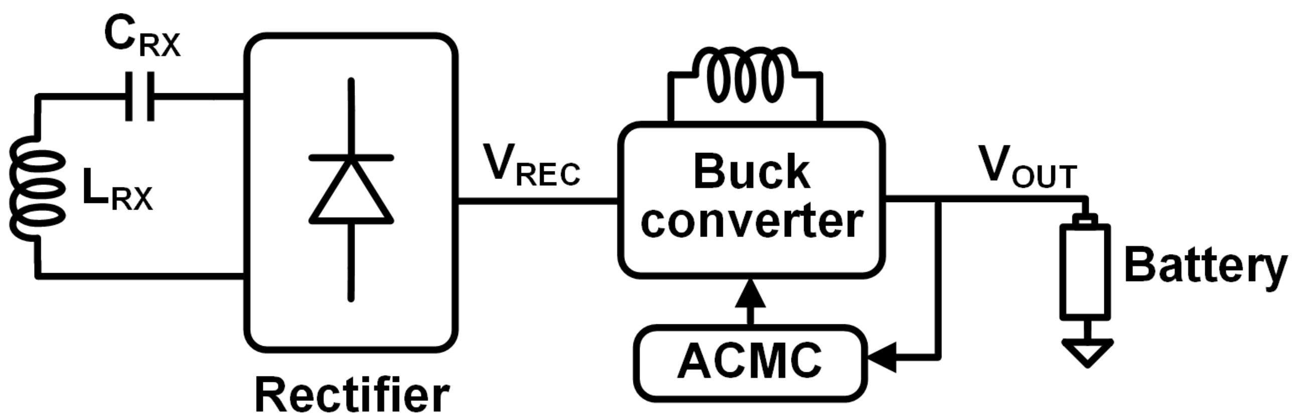
The PCE can be improved by using a high-efficiency post-regulator, e.g., a DC–DC converter. The authors in [16] showed a rectifier cascaded by a buck converter for battery charging as illustrated in Figure 6. Additionally, average current-mode control (ACMC) is applied for precise load current control in both continuous and discontinuous inductor current modes. With this topology, the measured rectifier efficiency and PCE were enhanced to 92.8% and 84.6%, respectively. However, additional bulky passive components, e.g., an off-chip inductor, are required in the DC–DC converter, resulting in a significant cost overhead and low integration. Moreover, the switching operation of the DC–DC converter increases the output ripple and ground noise.
2.1.3. The Rectifier Cascaded by an Inductorless Switching Converter
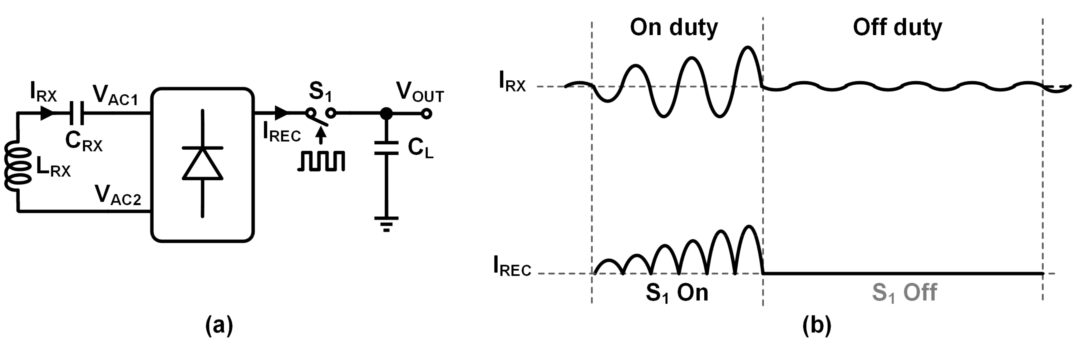
To eliminate the bulky inductor in [16], a resonant regulating rectifier (3R) was proposed in [17]. The working principle of this 3R scheme is illustrated in Figure 7a, where a switch S1 is inserted between the rectifier and the load. When S1 is turned on, the rectifier output current IREC charges the load (On duty in Figure 7b), while in the Off duty, S1 is turned off and the resonant current IRX freewheels without charging. Then, VOUT can be regulated by controlling the turn-on duty cycle of S1 using the pulse width modulation (PWM). During the off duty, the IREC reaches zero when S1 is turned off due to a very large equivalent resistance Req. Hence, the rectifier is working in Discontinuous Conduction Mode (DCM) similar to a DC–DC converter. This feature is not desirable, since the root meam square (RMS) resonant current IRX-RMS in this case will be much higher than that in Continuous Conduction Mode (CCM). This results in a higher coil power loss represented by IRX-RMS2×R2, where R2 represents the LRX resistance.
To reduce the RMS resonant current, a three-switch 3R scheme working in CCM was also presented in [17]. The working principle of this scheme is shown in Figure 8. When in on duty, both S1 and S3 are turned on and S2 is turned off, making CFL and CL connect in parallel. On the contrary, when in off duty, S1 and S3 are turned off and S2 is turned on, resulting in CFL and CL being connected in series. Under this configuration, a significantly smaller equivalent resistance Req can be achieved in off duty compared with DCM, allowing IREC to charge the load continuously similar to CCM as shown in Figure 8c. Similarly, the output voltage can be regulated using PWM to switch between the on- and off-duty states. However, considering DCM is still useful, especially under a light load condition, the three-switch 3R can also be configured to DCM by turning S1 and S3 on and S2 off in the on state and turning S1, S1, and S3 off in the off state. Hence, the load range can be extended by configuring the rectifier to DCM in light load conditions and CCM in heavy load conditions. This three-switch 3R showed a measured maximum 86% PCE when the loading current ranged from 70 to 700 mA, and precise regulation was achieved with a 3.3% output voltage deviation.
Another issue for the 3R scheme is that a potentially high VREC is expected at the beginning of off duty, which may damage the switches. To address this, a limiting capacitor CLM is added between the rectifier inputs (VAC1 and VAC2), which limits the VREC to VOUT + 2VD at on duty and VLM –2VD at off duty.
For the aforementioned post-stage regulations [12,13,14,15,16,17,18,19,20], they all suffer from loss from the cascaded stages. The PCE can be written as:
where ηrec and ηreg are the efficiencies of the rectifier and post-stage regulators, respectively. As such, although ηreg can be reasonably high, the PCE is still limited. Consequently, multiple one-stage regulation schemes have been proposed as a solution.
2.2. One-Stage Regulation
2.2.1. Active Diode Conduction Time Control
To eliminate the post regulator for a higher PCE, it is straightforward to integrate the rectification and regulation into one stage. The authors in [21,22,23] presented a one-stage regulating rectifier. In these schemes, the diode is implemented by a gate-controlled power transistor. The diode conduction time can be controlled by modulating the pulse width or the frequency of the power transistor gate control signal. As a result, the amount of current delivered to the load is controlled, and thus we have output regulation. These schemes are discussed as follows.
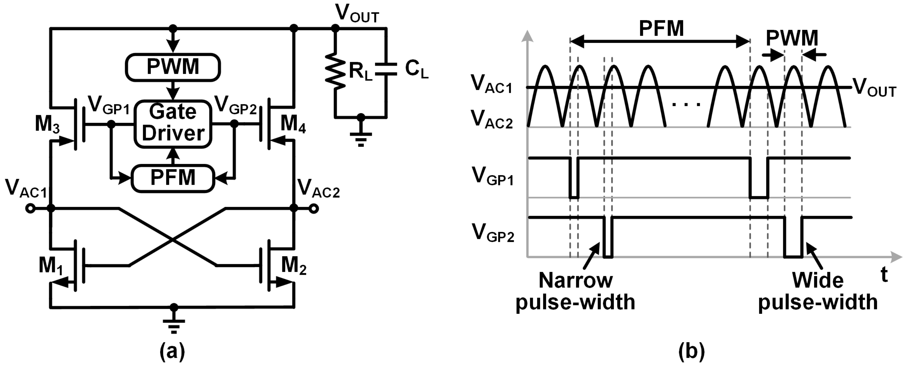
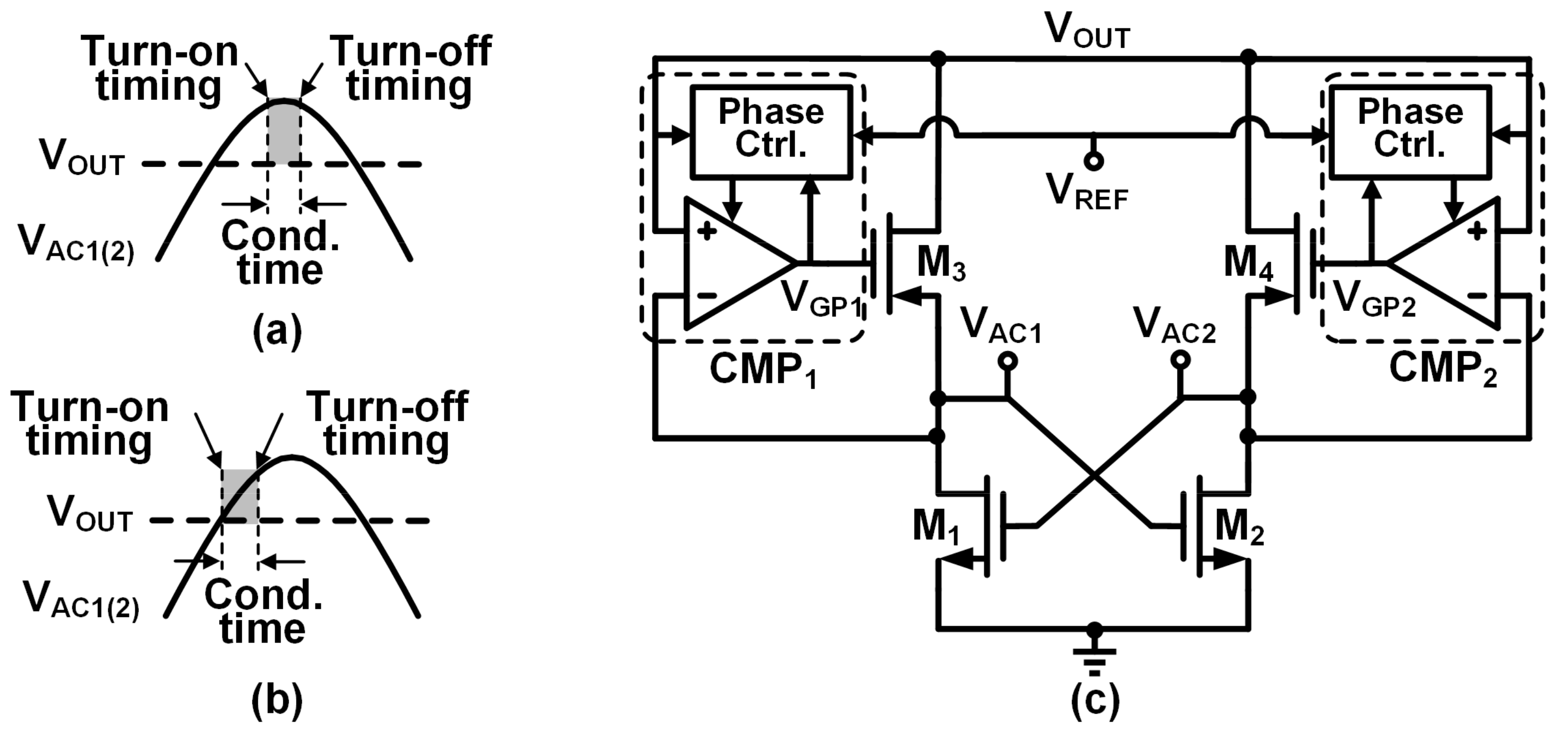
The authors in [21] proposed a regulating rectifier, and the regulation is achieved by controlling the active diode conduction time as in Figure 9a. The n-channel metal-oxide-semiconductor field-effect transistor (NMOS) M1 and M2 are cross-connected as the down rectifying diodes. For the up rectifying p-channel metal-oxide-semiconductor field-effect transistor (PMOS) M3 and M4, they are controlled by a pulse generator. When VAC1 > VOUT, M3 is turned off and M4 is turned on and vice versa. By controlling the M3 and M4 conduction time, VOUT regulation can be achieved. A PWM scheme will be straightforward, but the pulse width of the gate control signals VGP1 and VGP2 may be too narrow to turn on M3 and M4 under a light load condition for a high working frequency. To circumvent this, hybrid pulse modulation (HPM) is utilized as a combination of PWM and pulse frequency modulation (PFM) to provide regulation for a wide load range as given in Figure 9b. When the VGP1 and VGP2 pulse width controlled by PWM is decreased to a threshold value, PFM takes over the control loop by adjusting the VGP1 and VGP2 pulse frequency. The measurement result of [19] showed a maximum 60% PCE with a 10-mm coil distance. Obviously, the PCE is not optimized, which is mainly due to the relatively large rectifying diode drop (between VAC1(2) and VOUT) under certain loading conditions, especially when M3 and M4 may be turned on around the peak of VAC1(2) as in Figure 10a. As such, an additional power loss will be found on M3 and M4 and thus a PCE degradation.
To address this issue, the authors of [22], whose idea is illustrated in Figure 10c proposed a turn-on phase control technique to turn the active diodes on with a minimized diode drop. The M3 and M4 gate control signals in this scheme are generated by the phase control comparator CMP1 and CMP2 rather than a conventional comparator. The waveforms of VAC1(2) and VOUT are illustrated in Figure 10b. When VAC just exceeds VOUT, the rectifying diodes M3 and M4 are turned on, similar to a conventional rectifier, but they are turned off when VOUT exceeds a reference voltage VREF. Moreover, M3 and M4 also adopt a dynamic body biasing circuit for further voltage drop reduction and PCE improvement. The measurement results showed that this scheme can provide a regulated VOUT from 2.5 V to 4.6 V with an improved PCE from 72% to 87%.
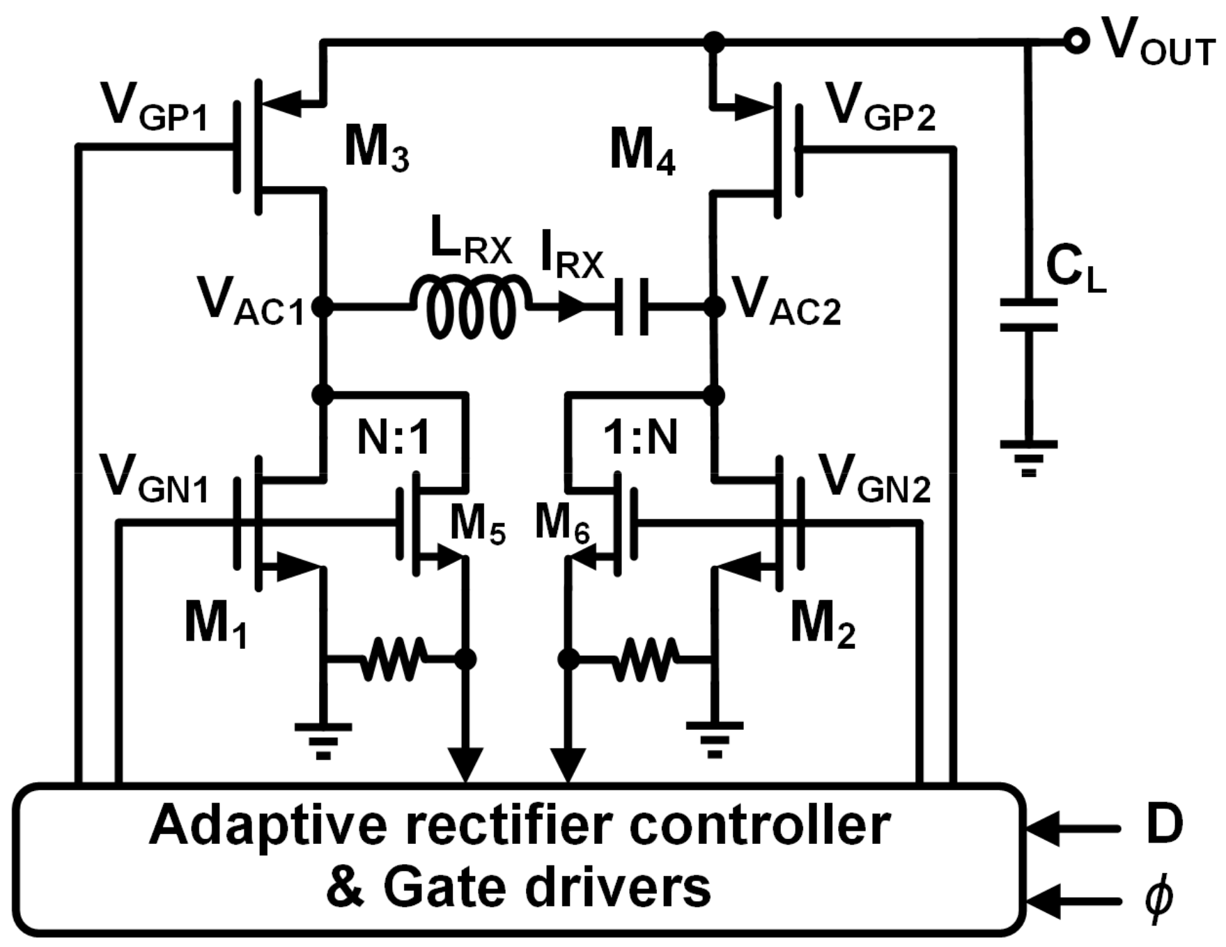
The PCE can be even more improved by optimizing the conduction time of both the up and down rectifying diodes [23] as in Figure 11. The VOUT regulation is achieved by adaptively adjusting the duty-cycle D and phase ϕ of the gate control signals VGP1, VGP2, VGN1, and VGN2 simultaneously with a rectification controller. The desired D and ϕ are adaptively synthesized based on an IRX sensor using M5 and M6. The measurement result showed that this phase and duty-cycle control can regulate the output voltage from 3.5 V to 5 V, and the maximum PCE was 96% at a 4.64 V output voltage.
2.2.2. Reconfigurable Regulating Rectification
Another one-stage topology is based on the reconfigurable resonant regulating (R3) rectification technique [24,25]. In these schemes, the R3 rectifier can be reconfigured to multiple basic rectifier topologies, e.g., full-wave (1×) and half-wave rectifiers (½×) and a voltage doubler (2×), and the rectifier output voltages are 1×, ½×, and 2× VOUT, respectively. As such, RX regulation can be achieved by switching among these topologies.
In [26,27], a 1×/2× reconfigurable rectifier was demonstrated as in Figure 12, where the switches S1~5 are utilized to fulfill the reconfiguration. When S3, S4 is turned on while the others are turned off, the power transistors M3 and M4 are cross-connected as two upper diodes, and D1 and D2 act as active diodes. In this scenario, it works as a full-wave rectifier as shown in Figure 12a. On the other hand, when S1 and S2 are turned on while S3 and S4 are turned off, M1 and M3 are configured to active diodes and M2 and M4 are disabled. Meanwhile, S5 is turned on to connect VAC2 to the middle of the two load capacitors CL1 and CL2, making the rectifier a voltage doubler as depicted in Figure 12b. It should be noted that Req equals RL/2 and RL/8 in 1× and 2× mode, respectively.
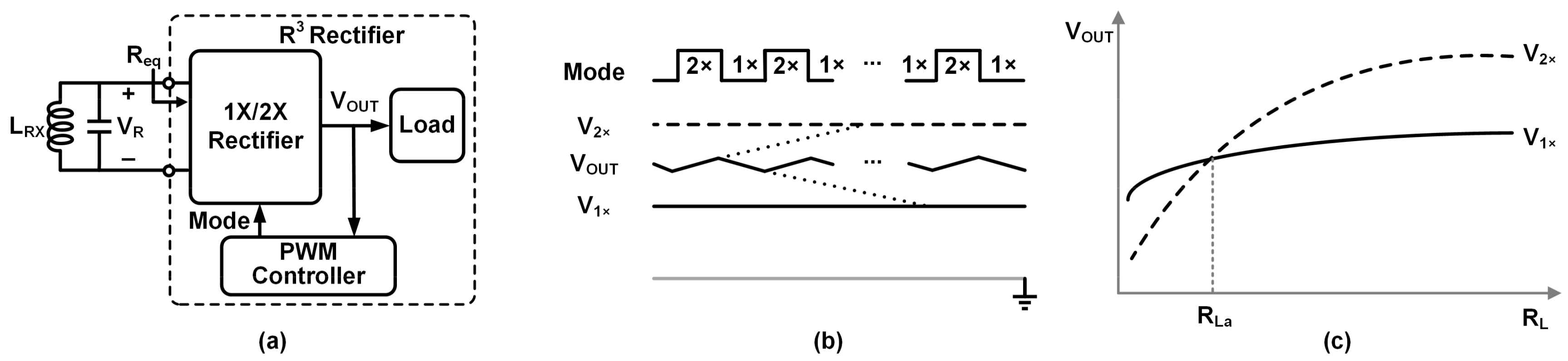
This reconfigurable rectifier topology was applied in [24] for regulation with PWM control as illustrated in Figure 13a. Once VAC1(2) has a fixed amplitude, the rectifier will output voltages V1× and V2× at 1× and 2× mode, respectively. As shown in Figure 13b, the PWM controller switches the reconfigurable rectifier periodically between the two modes so that VOUT can be regulated at an intermediate voltage between V1× and V2×. Thanks to the one-stage scheme, the maximum PCE of this R3 rectifier was 92.6% at a 60 mW output power in [24].
However, the R3 rectifier in [24] may fail to correctly regulate VOUT under certain circumstances. Firstly, VOUT cannot be regulated to lower than V1× or higher than V2×. Secondly, VOUT cannot be correctly regulated if the term V2× > V1× is not true, which is discussed as follows.
From [43], V2× andV1× can be written as:
where A is the voltage conversion ratio VOUT/VAC. From Equations (5) and (6), there exists a breakeven value where V2× = V1×, which can be given by:
and the resulting V1× and V2× versus the load is presented in Figure 13c. As can be seen, V2× > V1× will possibly take place under some heavy loading condition (RL < RLa), which undermines the regulation.
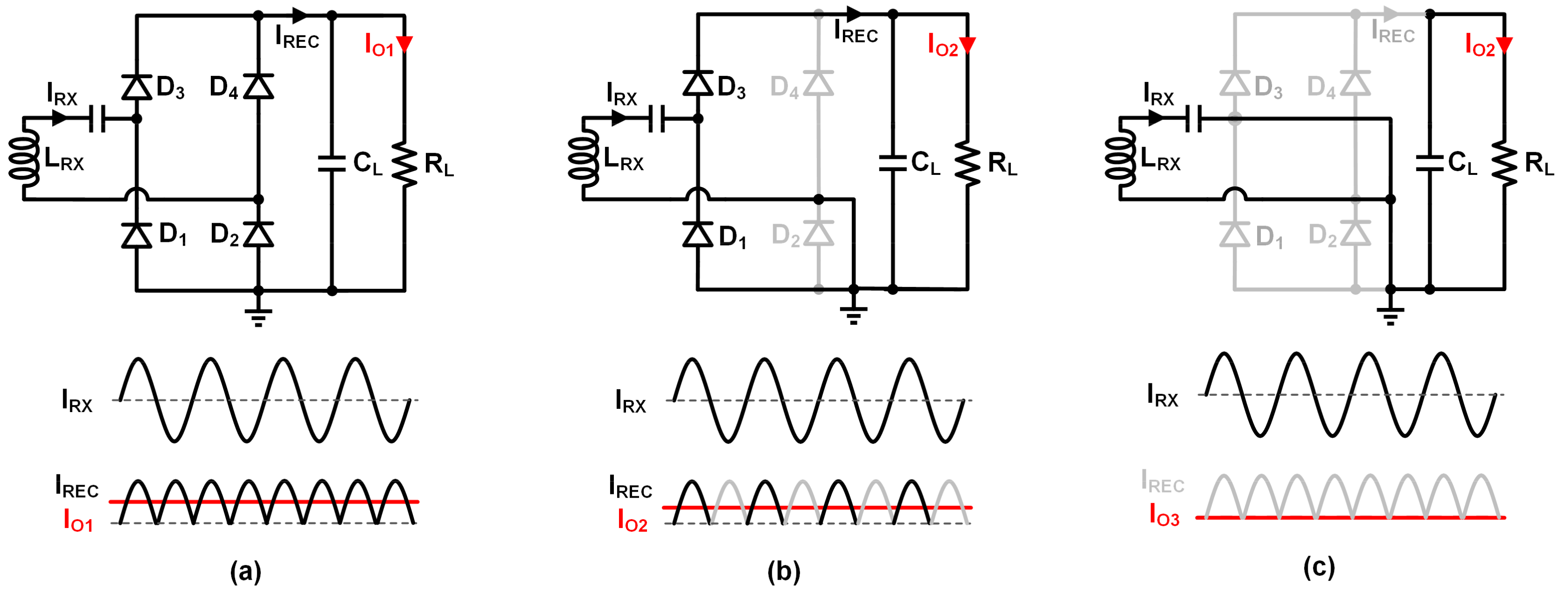
To overcome the limited load range and facilitate correct regulation, a three-mode R3 rectifier is presented in [25]. As illustrated in Figure 14, it can be configured into three modes: a full-bridge rectifier (1× mode), a half-bridge rectifier (½× mode), and freewheeling (0× mode). The ½× mode is added to fulfill an even distribution of power for a reduced output voltage ripples. The output regulation of this rectifier can be achieved by switching between two of the three modes. Specifically, it switches periodically between 1× and ½× mode under a heavy load, and between ½× and 0× mode under a light load. These two control schemes can be automatically changed based on the output current sensed. A first and Type II compensation are adopted in PWM to obtain a fast response and a stabilized system. A peak 92.2% PCE was measured with a 3.5 W output power, and a maximum 6 W output power was observed.
2.2.3. Switching-Based Current-Mode Regulation
To achieve a high VCE, a switching-based current-mode (SCM) regulating technique was proposed in [28,29,30,31]. This technique differs from voltage-mode ones by firstly storing the received energy in the RX LC resonant tank (as the resonant phase) and then delivering it to the load (charging phase). With SCM regulation, the power delivered to the load (PDL) can be regulated by controlling the length of the resonant phase.
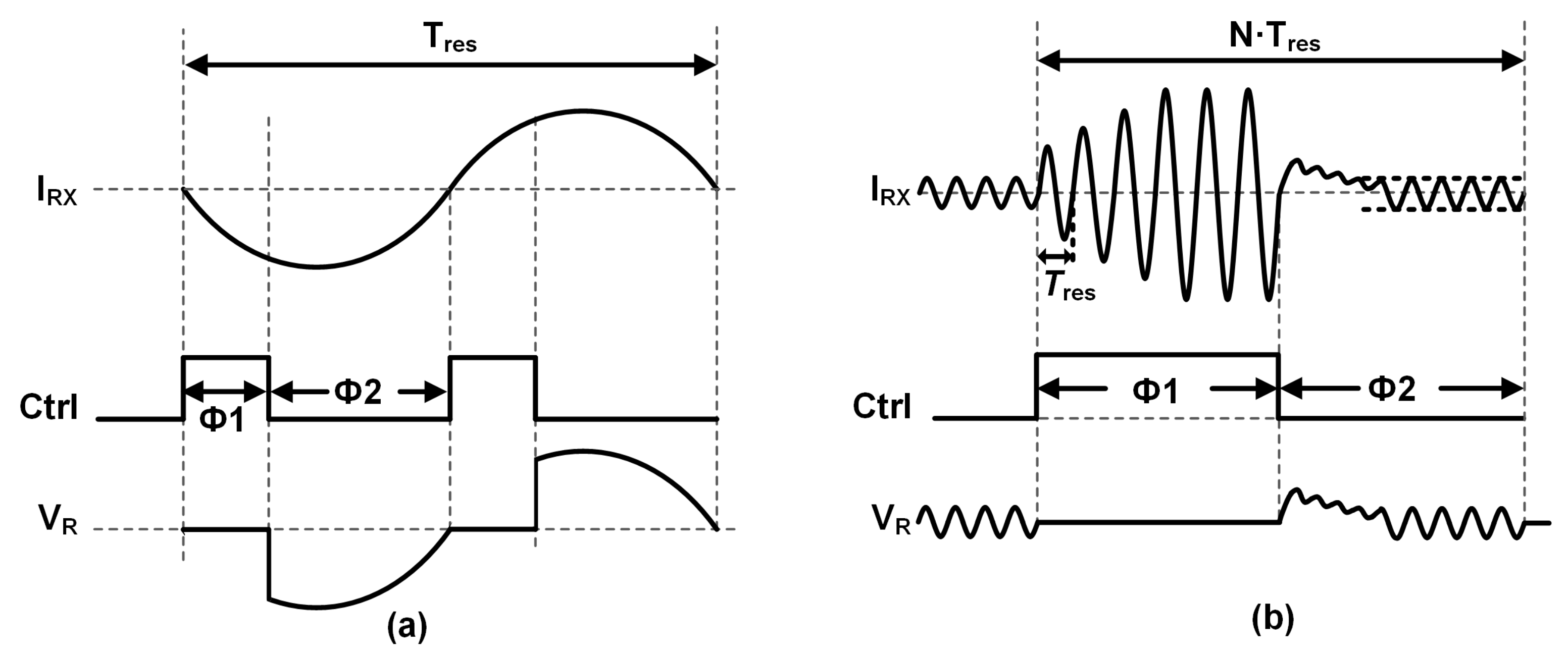
A SCM RX based on Q-modulation was proposed in [28] as in Figure 15a, where the regulation is realized by modulating Qload. As in Figure 15b, the resonant phase (with TΦ1 duration) is activated by turning on the single switch S1. For maximum energy storing, S1 is turned on at the zero-crossing point of the resonant current IRX, as in Figure 16a, which should be twice every cycle. Additionally, when SW is turned off, it is in a charging phase (with TΦ2 duration) as in Figure 15c.
Two advantages can be found in this SCM RX. For one thing, the equivalent resistance Req and thus the Q-factor are modulated by the duration ratio (m = TΦ1/TΦ2) as
where D = m/(1 + m). Consequently, by adjusting m, the received and thus output power can be regulated. For the other thing, according to Equation (8), the equivalent resistance Req is decreased in Q-modulation, and thus the Qload is increased. The VR in this case can be expressed as:
indicating that VR can be boosted without using a bulky inductor as in a conventional boost DC–DC converter. The measured results showed that the VR can be boosted to 5.5 V.
However, when maximum energy is stored in the LRXCRX tank, the SW turn-on timing should be restrictively synchronized to the IRX zero-crossing point, which significantly increases the design difficulty. In addition, this synchronization makes it difficult for the system to work at a high resonant frequency, e.g., the 2 MHz resonant frequency in [28]. The measured result showed that the PTE was 40.5% at RL = 200 Ω with an 8-cm coil distance, and greater than 20% PTE can be achieved when RL ranges from 50 to 1000 Ω.
To allow for a higher resonant frequency, a multi-cycle Q-modulation (MCQ) technique was introduced in [30] that works at a 13.56 MHz resonant frequency. The principle of MCQ is similar to that of [28], but both the resonant and charging phase are extended to multiple carrier cycles as in Figure 16b. MCQ can work without synchronizing the SW turn-on instant to the IRX zero-crossing points, which reduces the design difficulty. To overcome resonant frequency shifting due to the parasitic capacitance in the wireless link, an automatic resonance tuning scheme is also introduced in [30]. The measured result showed a 28.02% PTE at RL = 100 Ω. Compared with a voltage-mode rectifier, the VOUT has been increased significantly from an average of 2.61 to 4.15 V with the same input, coupling, and loading conditions.
In sum, the SCM technique can achieve a high VR without a voltage doubler or boost converter. This is due to the fact that the high-Q resonant tank is established by reducing the load in the resonant phase such that the VR can be much higher, resulting in a high output voltage delivered to the load. In addition, output regulation can be achieved by modulating Req. Unfortunately, in many cases PDL regulation and PTE optimization cannot be simultaneously achieved.
Table 1 presents a comparison of the RX regulation topologies used in state-of-the-art works. For the post-stage regulation, although they have a high rectifier efficiency, PCEs are limited due to the loss from the cascaded stage. By contrast, the one-stage schemes typically achieve a higher PCE, except [19] where a large rectifying diode drop takes place. In addition, to address the low VCE of the regulating rectifiers [21,22,23,24,25], the SCM technique is proposed in [28,31] to boost the VR. The VCE of [28] is still smaller than 1 due to its application to RL in the range of hundreds of ohms and below, while it is much higher in [31] when applied to a low output power system.
3. TX Regulation
Besides regulation at the RX side, the output can be regulated at the TX side as well. This scheme is defined as TX regulation, which can be achieved by controlling the PA supply voltage [24,32,33], the resonant frequency [34], or the power switch duty cycle [36,37,38,39,40]. The necessity for TX regulation and its implementations are discussed in the following sections.
3.1. Why TX Regulation is Necessary
TX regulation is pivotal in many cases. For one thing, TX regulation manages to widen the load range considering that the RX regulation range is typically limited. For the other thing, it is difficult to simultaneously optimize the PTE with RX regulation under a wide range of coil coupling distances, misalignments, or loading conditions. Hence, to optimize the PTE, TX regulation based on global feedback from the RX side is necessary.
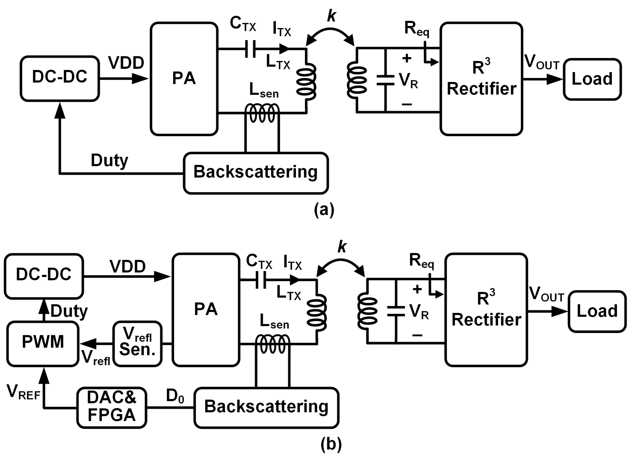
The authors in [24] presented a scenario for how TX regulation is useful to extend the output range, where V2× < V1× and thus false regulation may take place under certain load conditions. To handle this, the TX output power was increased during the 2× mode to ensure that V2× > V1× was unconditionally correct. The load condition at the RX side can be fed back to the TX side to facilitate TX power control. As shown in Figure 17a, the feedback is achieved with a global control loop, and the load condition can be sensed by a backscattering technique. Then, the significant difference of Req between 1× and 2× mode is backscattered to the primary side, causing an ITX difference, which is sensed by an additional coil Lsen coupling to the TX coil. This additional coil only takes up a small area so as to minimize its effect on the coupling coefficient and the cost overhead.
The authors in [32] demonstrated another TX regulation scheme to ensure V2× > V1×. Based on the analysis in [32], the VR is approximately proportional to Vrefl, which means that VR can be indirectly regulated by regulating Vrefl at the TX side instead. In this scheme, a fixed VR can be achieved over a much wider workable coupling and loading range. Within this range, V2× is approximately twice V1×, leading to correct output voltage regulation.
To regulate Vrefl, it must be sensed first. Unfortunately, Rrefl is not a physical resistor, so Vrefl cannot be sensed directly. Hence, as illustrated in Figure 17b, a current-based Vrefl sensor is applied for Vrefl detection. Then, by adjusting the supply voltage using a PWM-controlled DC–DC converter, the Vrefl can be regulated to be equal to reference voltage VREF under different modes in an R3 rectifier, keeping VR constant. In addition, the mode switching information D0 can feed back by backscattering and then convert into VREF by DAC (digital to analog converter) and FPGA (field programmable gate array). Measurement results showed that with this TX regulation, the workable coupling and loading ranges were extended by 250% with 120 mW output power and by 300% with a 1.2-cm coil distance compared to [24]. In addition, a maximum 92.5% PCE and 62.4% PTE were achieved.
3.2. Power Amplifier Supply Voltage Control
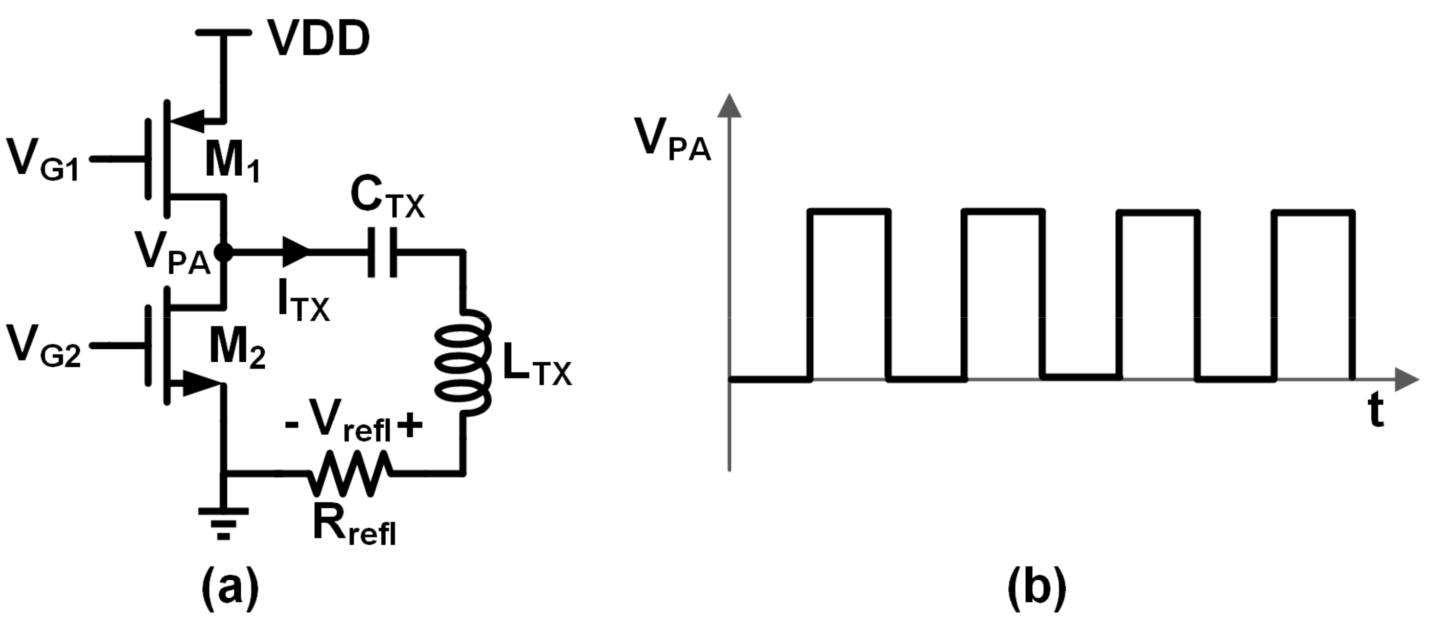
The PA supply voltage control, which is typically achieved with a DC–DC converter [33], is the most straightforward approach to TX regulation. Let us take a TX based on a class D PA as an example. As shown in Figure 18a, by setting a proper VG1 and VG2 to drive the M1 and M2, the PA will output a square wave VPA with a 50% duty cycle as in Figure 18b, and the Fourier series of VPA can be expressed as:
where ωsw = 2πfsw and fsw is the switching frequency. It is noteworthy that here n is an odd number. Then, the DC and high order harmonics components are filtered out by the LTXCTX tank. Consequently, the PA output voltage VPA is proportional to the supply voltage from Equation (10), and thus VPA can be regulated by controlling the supply voltage. Measurement results in [33] showed that a 40.2% PTE improvement had been achieved with a 7-mm coil distance and 250 mW output power.
3.3. Resonant Frequency Control
It should be noted that TX regulation can be achieved not only by adjusting the supply voltage, but also the resonant frequency fres. The more fres is tuned to be deviated from the resonant frequency of the LTXCTX tank, the less power will be transmitted.
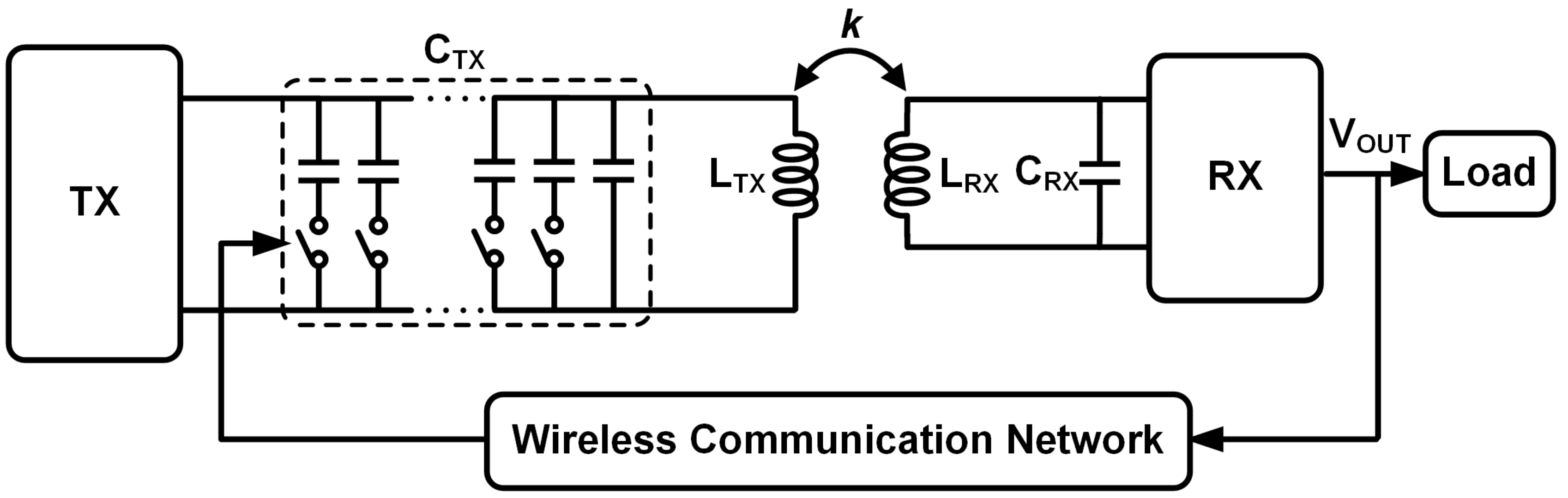
The authors in [34] presented a resonant frequency control scheme as illustrated in Figure 19. The resonant frequency here was adjusted by controlling the value of the capacitor CTX in the resonant TX tank. The CTX implements a weighted-capacitor array, which is controlled dynamically by the load condition from the RX side through a wireless communication network. The measurement results showed that the PDL can be regulated effectively over a wide load range, and 80% PCE can be achieved when transferring 15 W over a 10-mm coil distance.
Nonetheless, the CTX in [34] can only be tuned discretely, which prevents high-resolution regulation. Furthermore, for the commonly used megahertz Industrial Scientific Medical (ISM) band, the allowable bandwidth is pretty narrow, e.g., 15 KHz for 6.78 MHz and 7 KHz for 13.56 MHz [44]. Consequently, the tunable fres and regulation range will be limited to accommodate the ISM specifications. Additionally, a low PTE is expected, since the resonant frequency of the TX LC tank is purposely adjusted to deviate from the RX tank’s resonant frequency for regulation [43].
3.4. PA Power Switch Duty-Cycle Control
TX regulation can also be implemented by a PA power switch duty-cycle control technique based on switching frequency modulation [35,36], pulse density modulation [37,38], and phase shifted modulation [39,40]. These schemes advance the resonant frequency control scheme by keeping a constant fres. These schemes are discussed in the following sections.
3.4.1. Switching Frequency Modulation
It should be noted that fsw can be also designed to not be equal to fres. According to Equation (10), when fsw = fres/n, the nth subharmonic component can be used for the power transmission. Considering that the DC and other components are filtered out by the TX resonant tank, Vrefl can be written as:
According to Equation (11), Vrefl is proportional to fsw. Therefore, changing fsw according to the global feedback manages to regulate Vrefl and thus VOUT.
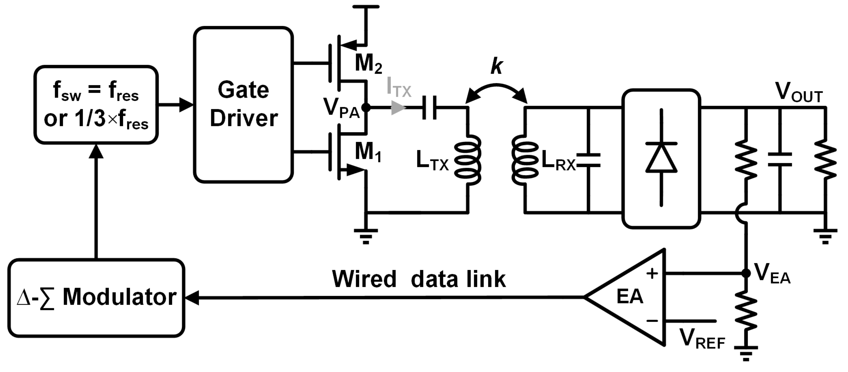
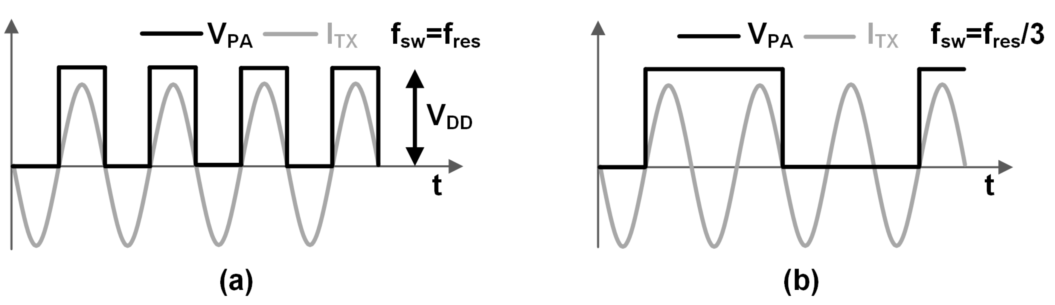
The authors in [35] demonstrated a switching frequency modulation technique as illustrated in Figure 20. In this work, the PA switching frequency fsw can be set to fres or fres/3 as shown in Figure 21a,b, respectively. Based on Equation (11), the Vrefl under fsw = fres/3 is 1/3 of that when fsw = fres. Hence, Vrefl can be regulated by switching fsw between fres and fres/3 using a PWM scheme while the resonant frequency is kept constant. Additionally, the error amplifier (EA) output is fed back to TX through the wired data link, and a 2nd Δ-Σ modulator is applied to switch the PA between the fres and fres/3 modes to reduce spurious emission. However, the regulation range is limited from fres/3 to fres. The measured results showed that maximum power of 0.52 W can be transferred with a 50% PTE.
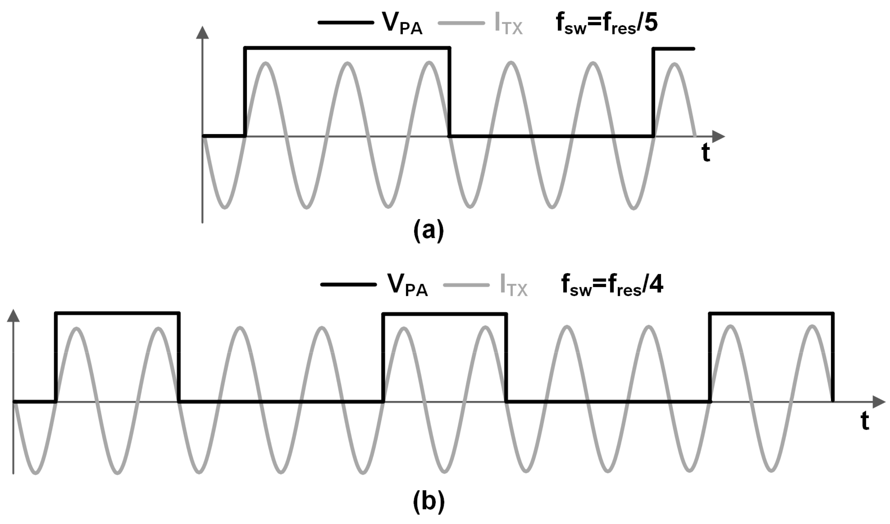
To extend the regulation range, [36] presented an enhanced subharmonic resonant switching scheme. Different from [35], the regulation can be achieved not only using odd-order harmonics, but also even-order harmonics. An even-order harmonic is implemented by averaging the adjacent two odd-order harmonics in the time domain, e.g., fres/4 can be achieved by averaging out fres/3 and fres/5 as illustrated in Figure 22b. As such, any frequency within (0, fres] can be chosen as fsw, resulting in a wider VOUT regulation range. The measurement results showed a 50% VOUT regulation range extension with the proposed scheme compared to [35].
3.4.2. Pulse Density Modulation
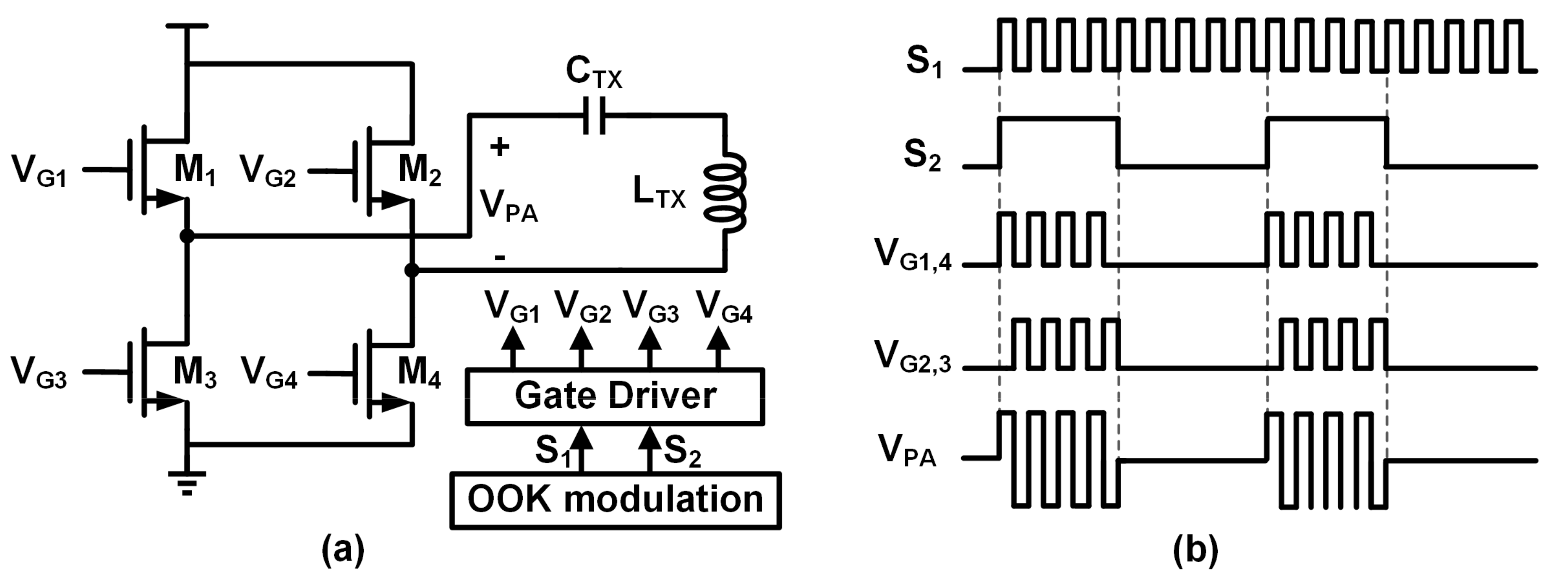
The authors in [37] showed a pulse density modulation (PDM) technique based on On-Off Keying (OOK) modulation. This scheme regulates the transmitted power by switching the PA between the working and idle modes using OOK modulation. As illustrated in Figure 23, the differential PA consists of four power switches M1~4, which are driven by the gate control voltages (VG1~4) with the resonant frequency. The switching signal S1, modulated with an OOK envelope S2, are applied to generate the gate control signals VG1~4. When S2 is logic high, the PA operates normally and when VLF is logic low, the PA operates in idle mode. The measured maximum PTE was 72.6% at a 10 Ω load resistance with a 0.2-m coil distance.
The authors in [35] proposed another PDM technique for both differential PA output voltage VPA regulation and optimized efficiency as illustrated in Figure 24a. This scheme regulates VPA by adjusting the pulse density d, which is defined as the total density of the positive (P) and negative (N) pulses of the voltage VPA, e.g., Figure 24b shows a VPA waveform when d = 1, while Figure 24c shows the d = 0.5 scenario, where some pulses are removed and denoted by “0”. Considering the root-mean-square (RMS) value of the VPA fundamental component is:
VPA can be well-regulated with any specified d within the range of [0, 1]. The measured results showed that this scheme maintained a constant output power of 10 W and achieved a maximum efficiency from 93% to 73% when the coil distance varied from 0.1 to 0.4 m under a 100 Ω load resistance. In addition, the gate control voltages VG1~4 are controlled by a specially designed ΔΣ-modulator to maintain the PA’s stability.
3.4.3. Phase-Shifted Modulation
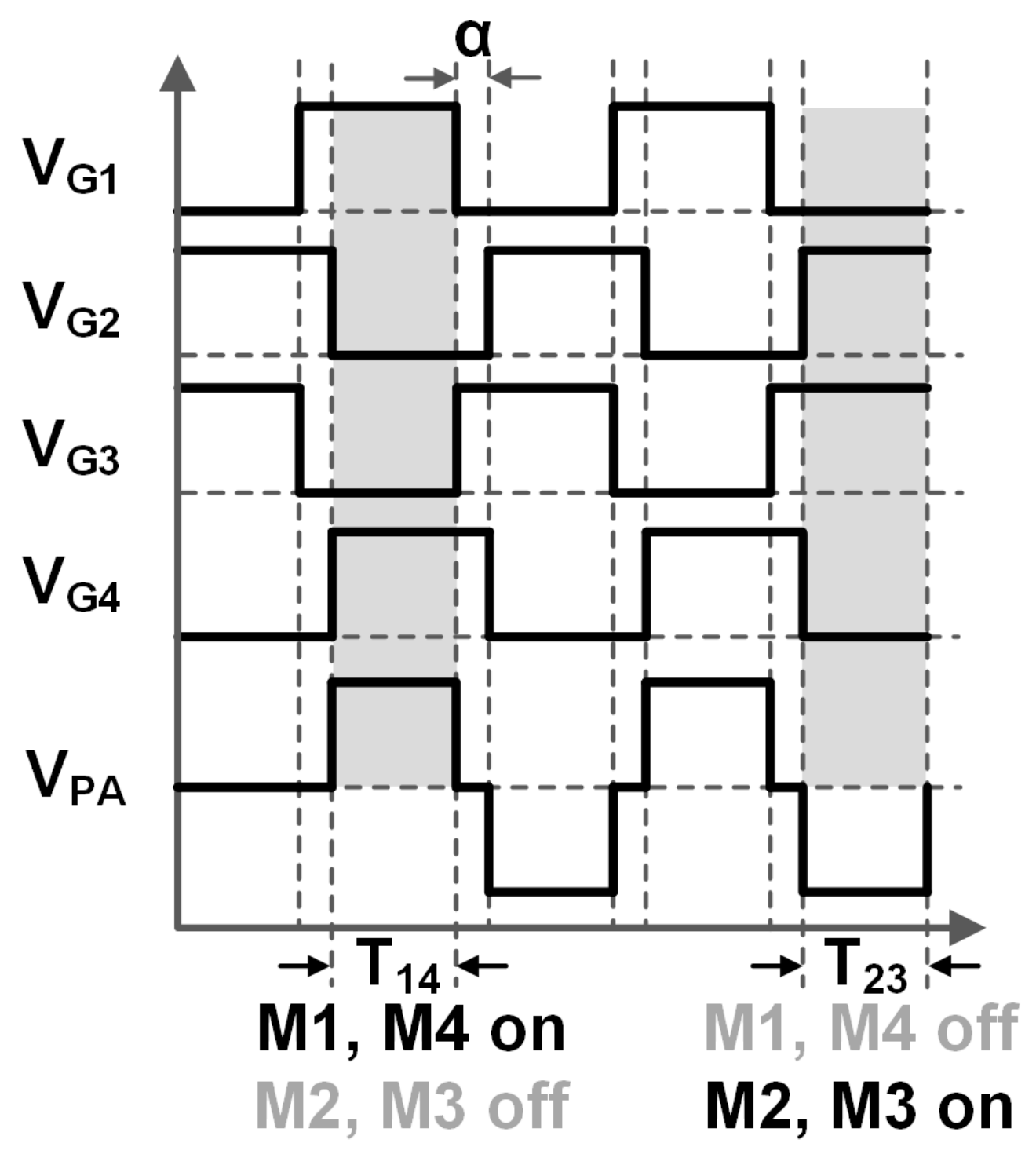
The authors in [36] presented a scheme that regulates the output voltage VPA by varying the phase-shifted angle α of the gate control signals VG1~4 in differential PA. As shown in Figure 25, the duty-cycle of each switching signal VG1~4 is 50%, but pulses of switch for M4 and M2 can lag M1 and M3 at a certain phase angle α ranging from 0° to 180°. Hence, by increasing α between VG1(2) and VG4(3), the simultaneous conduction time T14(23) of the power transistors M1(2) and M4(3) will be reduced, and thus the VPA will be decreased. The measured results demonstrated that the VPA was regulated to 28 V (rms) when the supply voltage ranged from 35 to 75 V, and the PA efficiency was around 94.5%.
However, the PA switching loss increases as the phase-shifted angle α approaches 180°, which results in a low efficiency under a light load condition. To address this, [40] demonstrated a TX regulation with harmonic-based phase-shifted modulation (HPSM). This technique applies the nth harmonic component of the switching frequency to regulate the transmitted power, as shown in Figure 26b, taking the 3rd HPSM as an example as follows.
A half-switching period is subdivided into six stages. Stage 1 [t0, t1]: M2 is turned on, the power is oscillating freely through M2, LTX, CTX, and D1, and VPA is equal to 0. Stage 2 [t1, t2]: M1 is turned on, the power is oscillating freely through M1, CTX, LTX, and D2, and VPA is equal to 0. Stage 3 [t2, t3]: M2 is turned off, the power is oscillating freely through M1, CTX, LTX, and D2, and VPA is still equal to 0. Stage 4 [t3, t4]: M4 is turned on, the power is transferred from the supply voltage to the ground through M1, CTX, LTX, and M4, and VPA is equal to VDD. Stage 5 [t4, t5]: the ITX changes its direction, the power is circulated from the ground to the supply voltage through D4, LTX, CTX, and D1, and VPA is equal to VDD. This stage finishes when ITX reaches zero. Stage 6 [t5, t6]: the ITX changes its direction again, and the power is transferred from the supply voltage to the ground through M1, CTX, LTX, and M4. As a result, the current ITX circulates three times during one switching period, which means lower switching loss compared with [39].
For higher-order harmonic control, there will be more current circulation per period and thus much lower switching loss, but smaller output power. The measurement results showed that HPSM with the 3rd harmonic component can improve PA efficiency by 10% compared to fundamental-based phase-shifted modulation.
3.5. Vector Power Summing Control
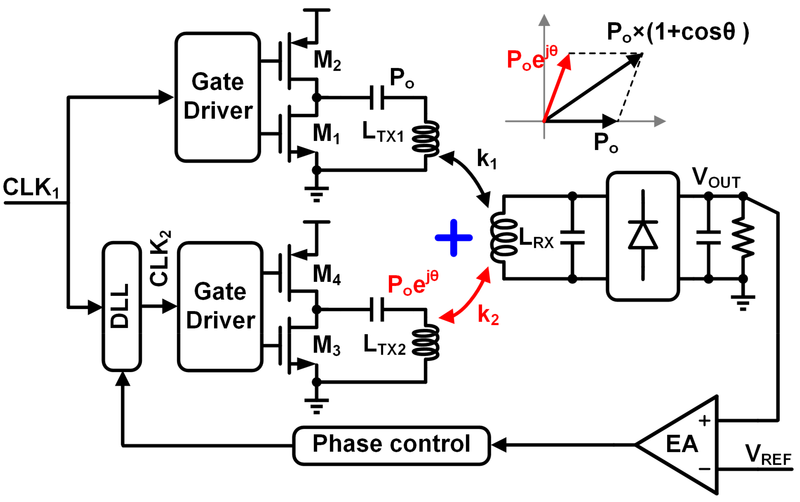
The aforementioned forms of TX regulation [32,33,34,35,36,37,38,39,40] are achieved only with a single TX, while it can also be implemented by summing the power from multiple TXs. The authors in [41,42] presented a vector power summing control technique to regulate the received power Ptotal as demonstrated in Figure 27. In this scheme, two power vectors, implemented by separate TXs, are then summed at a single RX. The two TXs are driven by two switching clocks (CLK1 and CLK2) with different phase θ under the same switching frequency (fsw = 1/Tsw). As a result, two transmitted powers, Po and Poejθ, are achieved in the two physically overlapped TX coils LTX1 and LTX2, respectively. Additionally, the transmitted power combined can be written as:
From Equation (13), the transmitted power can be regulated by controlling θ using a delay locked loop (DLL) and phase control circuit based on global feedback from the RX. In addition, wireless data communication can be simultaneously achieved using this vector summing technique [42].
Nevertheless, the vector summing technique will lead to a higher loss and system complexity due to the multiple TXs used. The measurement results showed that VOUT can be regulated from 3.3 to 16.3 V with 1 W output power and 50% PTE. Also, boosting up to 20 V was achieved at a 0.6 W power transfer without a boost-type DC–DC converter or charge pump circuit. Additionally, a 35 μs response time was measured against a 1 ms load fluctuation interval.
Table 2 gives a comparison of the TX regulation topologies among state-of-the-art works, where all achieve reasonably good PTE. For the supply voltage control scheme, it is the most straightforward approach to TX regulation. However, the switching loss can be further reduced by maintaining a low PA switching frequency, while using its subharmonic component as the resonant frequency, as in the PA duty-cycle control scheme. For the other two schemes, the narrow ISM bandwidth limits the performance of the fres control scheme, while an additional TX requirement undermines the vector power summing control scheme.
4. Discussions and Development Trends
For the resonant coupling WPT systems, as reviewed in this paper at the circuit level, output regulation can be achieved by post-stage regulation and one-stage regulation at the RX side as well as PA supply voltage control, resonant frequency control, duty-cycle control, and vector power summing control at the TX side.
For RX regulation, due to the poor efficiency of post-stage regulation, one-stage regulation, such as active diode conduction time control and R3 rectifier schemes, has been proposed for high PCE. However, the shortcoming of one-stage regulation is that the VCE is always smaller than 1.
Another one-stage regulation based on the switching-based current-mode (SCM) technique adopts the switching control method to utilize power transfer within two phases: store energy in the RX LC tank and then deliver the energy to the load. As a result, the voltage across the resonant RX tank can be boosted and this technique allows a >1 VCE at the RX side, which is thus suitable for a high-voltage application. Although the output regulation can be achieved by modulating the Req, the PTE is still unoptimized.
There are two disadvantages for RX-only regulation schemes. For one thing, the RX output may fall outside of regulation considering a limited RX regulation range. For the other thing, the regulation may deviate the Rrefl from the one for an optimal PTE considering that the loading and coupling conditions vary. Hence, TX regulation that optimizes the PTE based on global feedback from the RX side is also necessary.
For TX regulation, the PA supply voltage control scheme, typically implemented with a DC–DC converter, is straightforward but has relatively low efficiency and high cost. Another TX regulation scheme is resonant frequency control, based on a binary-weighted capacitor array, but its low resolution and high cost limit its further application. PA switching duty-cycle control is an effective way to achieve a continuously adjustable output, but zero voltage/current switching is required for high efficiency. In addition, a vector power summing scheme can also fulfill output regulation, but the regulation accuracy and efficiency are not favorable.
Moreover, for all of the TX regulation schemes, a global control loop is required to feed the RX output information back to the TX side through a data uplink channel. As such, the load transient response speed depends not only on the bandwidth of the global feedback loop, but also the data rate of the uplink channel. The data uplink telemetry can be implemented either in wired [17,35,41] or wireless ways. The wireless uplink schemes include Bluetooth, which has already be applied in A4WP [16,37], and backscattering based on load shift keying (LSK) [24,32,33].
To simplify the design of the binary-weighted capacitor array used in the resonant frequency control, a single phase switched fractional capacitor can be adopted for TX regulation by using the resonant frequency trimming technique as given in [45].
Another potential regulation topology is that the automatic maximum efficiency point tracking method [46] is implemented at the RX side and the regulation is achieved at the TX side. With this combined topology, the PTE can be optimized dynamically over a coupling and loading range with the help of TX regulation.
Last but not least, it is desirable to analyze the system stability and response speed because additional poles and zeros might be introduced with the regulation topologies.
5. Conclusions
In this work, the state-of-the-art regulation topologies in R-WPT systems for consumer electronics and bio-implants were comprehensively summarized and compared by mainly focusing on how to optimize the PTE, PCE, VCE, and PDL under loading or coupling variations. In addition, based on the advantages and drawbacks of these topologies, potential topologies are also proposed for researchers in this area. The regulation topologies design guidelines are not only suitable for R-WPT systems, but also for other near-field WPT systems.
Author Contributions
All authors conceived the work. The paper was written by Y.L. and revised by M.H. and B.L. The regulation topology classification and conclusion are suggested by Z.C. and X.Z.
Acknowledgments
This research is supported by the National Natural Science Foundation of China (61604044 and 61571196), the Fundamental Research Funds for the Central Universities (2017MS037), and the Science and Technology Project of Guangdong Province, China (2017B090908004, 2015B090901048).
Conflicts of Interest
The authors declare no conflict of interest.
References
- Chiaraviglio, L.; D’Andreagiovanni, F.; Lancellotti, R.; Shojafar, M.; Melazzi, N.B.; Canali, C. An Approach to Balance Maintenance Costs and Electricity Consumption in Cloud Data Centers. IEEE Trans. Sustain. Comput. 2018, 1–15. [Google Scholar] [CrossRef]
- Chiaraviglio, L.; Blefari-Melazzi, N.; Canali, C.; Cuomo, F.; Lancellotti, R.; Shojafar, M. A Measurement-Based Analysis of Temperature Variations Introduced by Power Management on Commodity Hardware. In Proceedings of the 2017 19th International Conference on Transparent Optical Networks (ICTON), Girona, Spain, 2–6 July 2017; pp. 1–4. [Google Scholar]
- Mayordomo, I.; Drager, T.; Spies, P.; Bernhard, J.; Pflaum, A. An Overview of Technical Challenges and Advances of Inductive Wireless Power Transmission. Proc. IEEE 2013, 101, 1302–1311. [Google Scholar] [CrossRef]
- Covic, G.A.; Boys, J.T. Inductive Power Transfer. Proc. IEEE 2013, 101, 1276–1289. [Google Scholar] [CrossRef]
- Agarwal, K.; Jegadeesan, R.; Guo, Y.X.; Thakor, N.V. Wireless Power Transfer Strategies for Implantable Bioelectronics: Methodological Review. IEEE Rev. Biomed. Eng. 2017, 10, 136–161. [Google Scholar] [CrossRef] [PubMed]
- Dai, J.; Ludois, D.C. A Survey of Wireless Power Transfer and a Critical Comparison of Inductive and Capacitive Coupling for Small Gap Applications. IEEE Trans. Power Electron. 2015, 30, 6017–6029. [Google Scholar] [CrossRef]
- Jiang, C.; Chau, K.T.; Liu, C.; Lee, C.H.T. An Overview of Resonant Circuits for Wireless Power Transfer. Energies 2017, 10, 894. [Google Scholar] [CrossRef]
- Zhou, D.D.; Greenbaum, E. Implantable Neural Prostheses 2: Techniques and Engineering Approaches; Springer: New York, NY, USA, 2010; ISBN 978-0-387-98119-2. [Google Scholar]
- Ishida, K.; Yasufuku, T.; Miyamoto, S.; Nakai, H.; Takamiya, M.; Sakurai, T.; Takeuchi, K. 1.8 V Low-Transient-Energy Adaptive Program-Voltage Generator Based on Boost Converter for 3D-Integrated NAND Flash SSD. IEEE J. Solid-State Circuits 2011, 46, 1478–1487. [Google Scholar] [CrossRef] [Green Version]
- Pagano, R.; Baker, M.; Radke, R.E. A 0.18-μm Monolithic Li-Ion Battery Charger for Wireless Devices Based on Partial Current Sensing and Adaptive Reference Voltage. IEEE J. Solid-State Circuits 2012, 47, 1355–1368. [Google Scholar] [CrossRef]
- Huang, M.; Lu, Y.; Seng-Pan, U.; Martins, R.P. 22.4 A Reconfigurable Bidirectional Wireless Power Transceiver with Maximum-Current Charging Mode and 58.6% Battery-to-Battery Efficiency. In Proceedings of the IEEE International Solid-State Circuits Conference (ISSCC), Digest of Technical Papers, San Francisco, CA, USA, 5–9 February 2017; pp. 376–377. [Google Scholar]
- Wu, C.Y.; Qian, X.H.; Cheng, M.S.; Liang, Y.A.; Chen, W.M. A 13.56 MHz 40 mW CMOS High-Efficiency Inductive Link Power Supply Utilizing On-Chip Delay-Compensated Voltage Doubler Rectifier and Multiple LDOs for Implantable Medical Devices. IEEE J. Solid-State Circuits 2014, 49, 2397–2407. [Google Scholar] [CrossRef]
- Lee, H. An Auto-Reconfigurable AC-DC Regulator for Wirelessly Powered Biomedical Implants With 28% Link Efficiency Enhancement. IEEE Trans. Very Large Scale Integr. VLSI Syst. 2016, 24, 1598–1602. [Google Scholar] [CrossRef]
- Kiani, M.; Lee, B.; Yeon, P.; Ghovanloo, M. 12.7 A Power-Management ASIC with Q-modulation Capability for Efficient Inductive Power Transmission. In Proceedings of the IEEE International Solid-State Circuits Conference (ISSCC), Digest of Technical Papers, San Francisco, CA, USA, 22–26 February 2015; pp. 226–228. [Google Scholar]
- Lee, H.M.; Ghovanloo, M. An Integrated Power-Efficient Active Rectifier with Offset-Controlled High-Speed Comparators for Inductively Powered Applications. IEEE Trans. Circuits Syst. Regul. Pap. 2011, 58, 1749–1760. [Google Scholar] [CrossRef] [PubMed]
- Moh, K.G.; Neri, F.; Moon, S.; Yeon, P.; Yu, J.; Cheon, Y.; Roh, Y. s; Ko, M.; Park, B.H. 12.9 A Fully Integrated 6W Wireless Power Receiver Operating at 6.78MHz with Magnetic Resonance Coupling. In Proceedings of the IEEE International Solid-State Circuits Conference (ISSCC), Digest of Technical Papers, San Francisco, CA, USA, 22–26 February 2015; pp. 230–232. [Google Scholar]
- Choi, J.-H.; Yeo, S.-K.; Park, S.; Lee, J.-S.; Cho, G.-H. Resonant Regulating Rectifiers (3R) Operating for 6.78 MHz Resonant Wireless Power Transfer (RWPT). IEEE J. Solid-State Circuits 2013, 48, 2989–3001. [Google Scholar] [CrossRef]
- Park, Y.J.; Jang, B.; Park, S.M.; Ryu, H.C.; Oh, S.J.; Kim, S.Y.; Pu, Y.; Yoo, S.S.; Hwang, K.C.; Yang, Y.; et al. A Triple-Mode Wireless Power-Receiving Unit With 85.5% System Efficiency for A4WP, WPC, and PMA Applications. IEEE Trans. Power Electron. 2018, 33, 3141–3156. [Google Scholar] [CrossRef]
- Moon, Y.J.; Roh, Y.S.; Yoo, C.; Kim, D.Z. A 3.0-W Wireless Power Receiver Circuit with 75-% Overall Efficiency. In Proceedings of the IEEE Asian Solid-State Circuits Conference (A-SSCC), Kobe, Japan, 12–14 November 2012; pp. 97–100. [Google Scholar]
- Park, H.G.; Jang, J.H.; Kim, H.J.; Park, Y.J.; Oh, S.; Pu, Y.; Hwang, K.C.; Yang, Y.; Lee, K.Y. A Design of a Wireless Power Receiving Unit with a High-Efficiency 6.78-MHz Active Rectifier Using Shared DLLs for Magnetic-Resonant A4WP Applications. IEEE Trans. Power Electron. 2016, 31, 4484–4498. [Google Scholar] [CrossRef]
- Kim, C.; Ha, S.; Park, J.; Akinin, A.; Mercier, P.P.; Cauwenberghs, G. A 144-MHz Fully Integrated Resonant Regulating Rectifier with Hybrid Pulse Modulation for Mm-Sized Implants. IEEE J. Solid-State Circuits 2017, 52, 3043–3055. [Google Scholar] [CrossRef]
- Lee, H.M.; Park, H.; Ghovanloo, M. A Power-Efficient Wireless System with Adaptive Supply Control for Deep Brain Stimulation. IEEE J. Solid-State Circuits 2013, 48, 2203–2216. [Google Scholar] [CrossRef] [PubMed]
- Ozalevli, E.; Femia, N.; Capua, G.D.; Subramonian, R.; Du, D.; Sankman, J.; Markhi, M.E. A Cost-Effective Adaptive Rectifier for Low Power Loosely Coupled Wireless Power Transfer Systems. IEEE Trans. Circuits Syst. Regul. Pap. 2017, 1–12. [Google Scholar] [CrossRef]
- Li, X.; Tsui, C.-Y.; Ki, W.-H. A 13.56 MHz Wireless Power Transfer System with Reconfigurable Resonant Regulating Rectifier and Wireless Power Control for Implantable Medical Devices. IEEE J. Solid-State Circuits 2015, 50, 978–989. [Google Scholar] [CrossRef]
- Cheng, L.; Ki, W.H.; Tsui, C.Y. A 6.78-MHz Single-Stage Wireless Power Receiver Using a 3-Mode Reconfigurable Resonant Regulating Rectifier. IEEE J. Solid-State Circuits 2017, 52, 1412–1423. [Google Scholar] [CrossRef]
- Lee, H.M.; Ghovanloo, M. An Adaptive Reconfigurable Active Voltage Doubler/Rectifier for Extended-Range Inductive Power Transmission. In Proceedings of the IEEE International Solid-State Circuits Conference (ISSCC), Digest of Technical Papers, San Francisco, CA, USA, 19–23 February 2012; pp. 286–288. [Google Scholar]
- Lu, Y.; Li, X.; Ki, W.H.; Tsui, C.Y.; Yue, C.P. A 13.56MHz Fully Integrated 1X/2X Active Rectifier with Compensated Bias Current for Inductively Powered Devices. In Proceedings of the IEEE International Solid-State Circuits Conference (ISSCC), Digest of Technical Papers, San Francisco, CA, USA, 17–21 February 2013; pp. 66–67. [Google Scholar]
- Kiani, M.; Lee, B.; Yeon, P.; Ghovanloo, M. A Q-Modulation Technique for Efficient Inductive Power Transmission. IEEE J. Solid-State Circuits 2015, 50, 2839–2848. [Google Scholar] [CrossRef] [PubMed]
- Ahn, D.; Kim, S.; Moon, J.; Cho, I.-K. Wireless Power Transfer with Automatic Feedback Control of Load Resistance Transformation. IEEE Trans. Power Electron. 2016, 31, 7876–7886. [Google Scholar] [CrossRef]
- Lee, B.; Yeon, P.; Ghovanloo, M. A Multicycle Q-Modulation for Dynamic Optimization of Inductive Links. IEEE Trans. Ind. Electron. 2016, 63, 5091–5100. [Google Scholar] [CrossRef] [PubMed] [Green Version]
- Gougheri, H.S.; Kiani, M. Current-Based Resonant Power Delivery with Multi-Cycle Switching for Extended-Range Inductive Power Transmission. IEEE Trans. Circuits Syst. Regul. Pap. 2016, 63, 1543–1552. [Google Scholar] [CrossRef]
- Li, X.; Tsui, C.Y.; Ki, W.H. 12.8 Wireless Power Transfer System Using Primary Equalizer for Coupling- and Load-Range Extension in Bio-implant Applications. In Proceedings of the IEEE International Solid-State Circuits Conference (ISSCC), Digest of Technical Papers, San Francisco, CA, USA, 22–26 February 2015; pp. 228–230. [Google Scholar]
- Wang, G.; Liu, W.; Sivaprakasam, M.; Kendir, G.A. Design and Analysis of an Adaptive Transcutaneous Power Telemetry for Biomedical Implants. IEEE Trans. Circuits Syst. Regul. Pap. 2005, 52, 2109–2117. [Google Scholar] [CrossRef]
- Si, P.; Hu, A.P.; Malpas, S.; Budgett, D. A Frequency Control Method for Regulating Wireless Power to Implantable Devices. IEEE Trans. Biomed. Circuits Syst. 2008, 2, 22–29. [Google Scholar] [CrossRef] [PubMed]
- Shinoda, R.; Tomita, K.; Hasegawa, Y.; Ishikuro, H. Voltage-Boosting Wireless Power Delivery System with Fast Load Tracker by ΔΣ-modulated Sub-Harmonic Resonant Switching. In Proceedings of the IEEE International Solid-State Circuits Conference (ISSCC), Digest of Technical Papers, San Francisco, CA, USA, 19–23 February 2012; pp. 288–290. [Google Scholar]
- Li, X.; Li, Y.P.; Tsui, C.Y.; Ki, W.H. Wireless Power Transfer System with ΔΣ-Modulated Transmission Power and Fast Load Response for Implantable Medical Devices. IEEE Trans. Circuits Syst. II Express Briefs 2017, 64, 279–283. [Google Scholar] [CrossRef]
- Zhong, W.; Hui, S.Y.R. Maximum Energy Efficiency Operation of Series-Series Resonant Wireless Power Transfer Systems Using On-Off Keying Modulation. IEEE Trans. Power Electron. 2018, 33, 3595–3603. [Google Scholar] [CrossRef]
- Li, H.; Wang, K.; Fang, J.; Tang, Y. Pulse Density Modulated ZVS Full-Bridge Converters for Wireless Power Transfer Systems. IEEE Trans. Power Electron. 2018. [Google Scholar] [CrossRef]
- Ye, Z.; Jain, P.K.; Sen, P.C. A Full-Bridge Resonant Inverter with Modified Phase-Shift Modulation for High-Frequency AC Power Distribution Systems. IEEE Trans. Ind. Electron. 2007, 54, 2831–2845. [Google Scholar] [CrossRef]
- Cai, H.; Shi, L.; Li, Y. Harmonic-Based Phase-Shifted Control of Inductively Coupled Power Transfer. IEEE Trans. Power Electron. 2014, 29, 594–602. [Google Scholar] [CrossRef]
- Tomita, K.; Shinoda, R.; Kuroda, T.; Ishikuro, H. 1W 3.3V-to-16.3V Boosting Wireless Power Transfer Circuits with Vector Summing Power Controller. IEEE J. Solid-State Circuits 2012, 47, 2576–2585. [Google Scholar] [CrossRef]
- Kosuge, A.; Hashiba, J.; Kawajiri, T.; Hasegawa, S.; Shidei, T.; Ishikuro, H.; Kuroda, T.; Takeuchi, K. An Inductively Powered Wireless Solid-State Drive System with Merged Error Correction of High-Speed Wireless Data Links and NAND Flash Memories. IEEE J. Solid-State Circuits 2016, 51, 1041–1050. [Google Scholar] [CrossRef]
- Van Schuylenbergh, K.; Puers, R. Inductive Powering: Basic Theory and Application to Biomedical Systems. In Analog Circuits and Signal Processing; Springer: Dordrecht, The Netherlands, 2009; ISBN 978-90-481-2411-4. [Google Scholar]
- Finkenzeller, K. Fundamentals and Applications in Contactless Smart Cards, Radio Frequency Identification and Near-Field Communication, 3rd ed.; Wiley: Chichester, UK; Hoboken, NJ, USA, 2010; ISBN 978-0-470-69506-7. [Google Scholar]
- Kennedy, H.; Bodnar, R.; Lee, T.; Redman-White, W. A self-tuning resonant inductive link transmit driver using quadrature-symmetric phase-switched fractional capacitance. In Proceedings of the IEEE International Solid-State Circuits Conference (ISSCC), Digest of Technical Papers, San Francisco, CA, USA, 5–9 February 2017; pp. 370–371. [Google Scholar]
- Mao, F.; Lu, Y.; Seng-Pan, U.; Martins, R.P. A Reconfigurable Cross-Connected Wireless-Power Transceiver for Bidirectional Device-to-Device Charging with 78.1% Total Efficiency. In Proceedings of the IEEE International Solid-State Circuits Conference (ISSCC), Digest of Technical Papers, San Francisco, CA, USA, 11–15 February 2018; pp. 140–142. [Google Scholar]
Figure 1.
The block diagram of a resonant wireless power transfer (R-WPT) system with series-resonant transmitter (TX) and receiver (RX) tanks.
Figure 1.
The block diagram of a resonant wireless power transfer (R-WPT) system with series-resonant transmitter (TX) and receiver (RX) tanks.

Figure 2.
(a) The circuit model of the R-WPT system with series-resonant TX and RX tanks, and (b) the effect of the RX’s resonant magnetic coupling with the TX is presented as a reflected resistance in the TX.
Figure 2.
(a) The circuit model of the R-WPT system with series-resonant TX and RX tanks, and (b) the effect of the RX’s resonant magnetic coupling with the TX is presented as a reflected resistance in the TX.
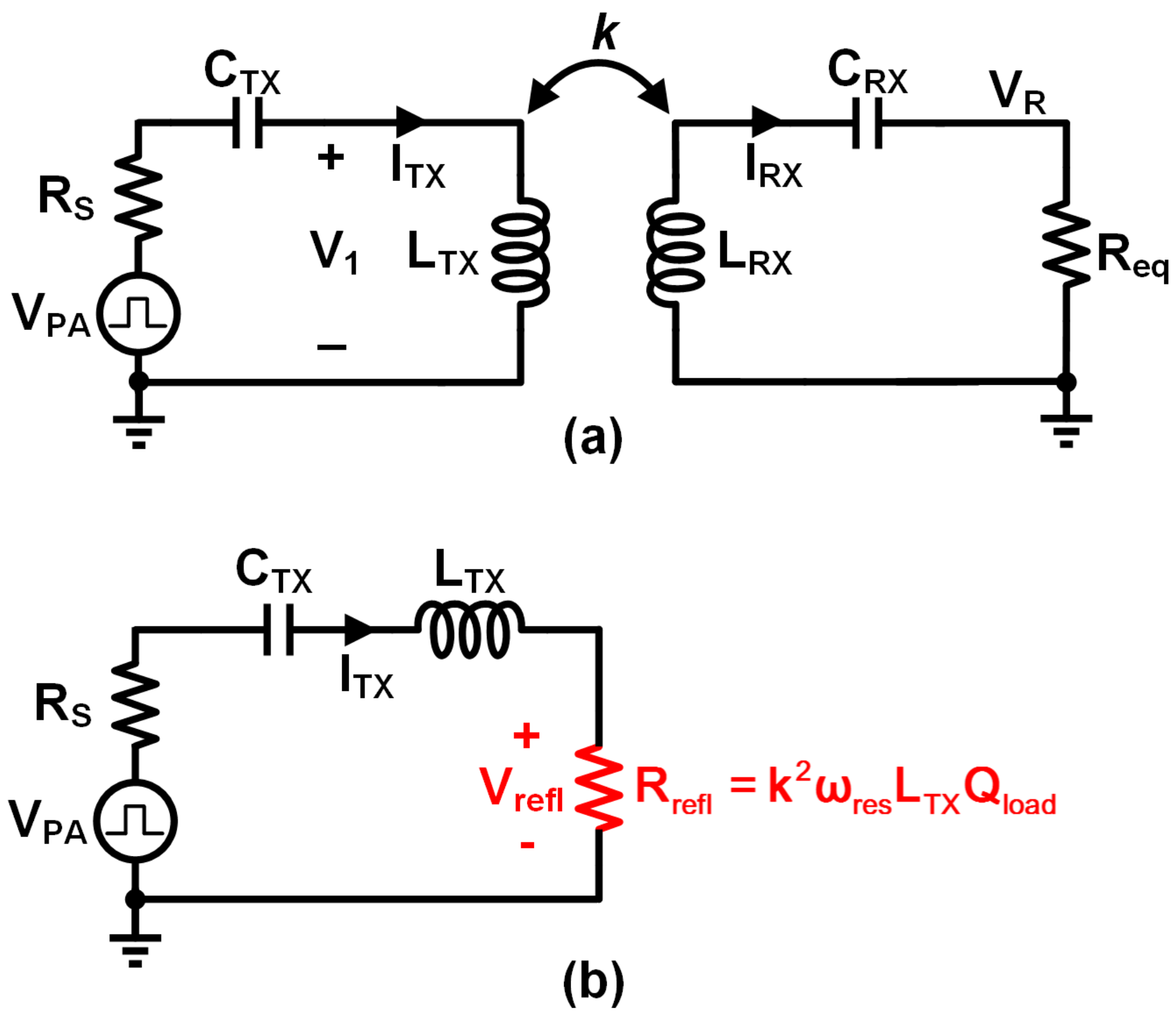
Figure 3.
The category of the regulation topologies. LDO, low dropout regulator; DC, direct current.
Figure 3.
The category of the regulation topologies. LDO, low dropout regulator; DC, direct current.

Figure 4.
The block diagram of an RX with post-stage regulation.

Figure 5.
The RX with cascaded LDOs [12]. ALDO, analog low dropout regulator; DLDO, digital low dropout regulator; RLDO, reference low dropout regulator.
Figure 5.
The RX with cascaded LDOs [12]. ALDO, analog low dropout regulator; DLDO, digital low dropout regulator; RLDO, reference low dropout regulator.

Figure 6.
The RX with cascaded a buck converter [16]. ACMC, average current-mode control.
Figure 6.
The RX with cascaded a buck converter [16]. ACMC, average current-mode control.

Figure 7.
(a) The schematic of a resonant regulating rectifier (3R); and (b) the switching waveforms of IRX and IREC, working in Discontinuous Conduction Mode (DCM) similar to a DC–DC converter [17].
Figure 7.
(a) The schematic of a resonant regulating rectifier (3R); and (b) the switching waveforms of IRX and IREC, working in Discontinuous Conduction Mode (DCM) similar to a DC–DC converter [17].

Figure 8.
The schematic of the three-switch 3R in (a) an on-duty state when S1 and S3 are turned on and S2 is turned off and (b) an off-duty state when S1 and S3 are turned off and S2 is turned on. (c) Switching waveforms of IRX and IREC in Continuous Conduction Mode (CCM) [17].
Figure 8.
The schematic of the three-switch 3R in (a) an on-duty state when S1 and S3 are turned on and S2 is turned off and (b) an off-duty state when S1 and S3 are turned off and S2 is turned on. (c) Switching waveforms of IRX and IREC in Continuous Conduction Mode (CCM) [17].

Figure 9.
(a) The schematic of a regulating rectifier based on the hybrid pulse modulation (HPM) technique; (b) The waveforms of VAC1, VAC2, VGP1, and VGP2, where a narrow and wide pulse width is expected under light and heavy load conditions, respectively [21]. PFM, pulse frequency modulation; PWM, pulse width modulation.

Figure 10.
The conduction time starts at (a) the peak of VAC1(2); and (b) VAC just exceeds VOUT; (c) The schematic of the regulating rectifier based on the turn-on phase control technique [22]. CMP, comparator.
Figure 10.
The conduction time starts at (a) the peak of VAC1(2); and (b) VAC just exceeds VOUT; (c) The schematic of the regulating rectifier based on the turn-on phase control technique [22]. CMP, comparator.

Figure 11.
The schematic of the adaptive regulating rectifier based on phase and duty-cycle control [23].
Figure 11.
The schematic of the adaptive regulating rectifier based on phase and duty-cycle control [23].

Figure 12.
1×/2× reconfigurable rectifier operates (a) in 1× mode; and (b) in 2× mode [26], active diodes are composed of the gate-controlled power transistor and comparator.
Figure 12.
1×/2× reconfigurable rectifier operates (a) in 1× mode; and (b) in 2× mode [26], active diodes are composed of the gate-controlled power transistor and comparator.
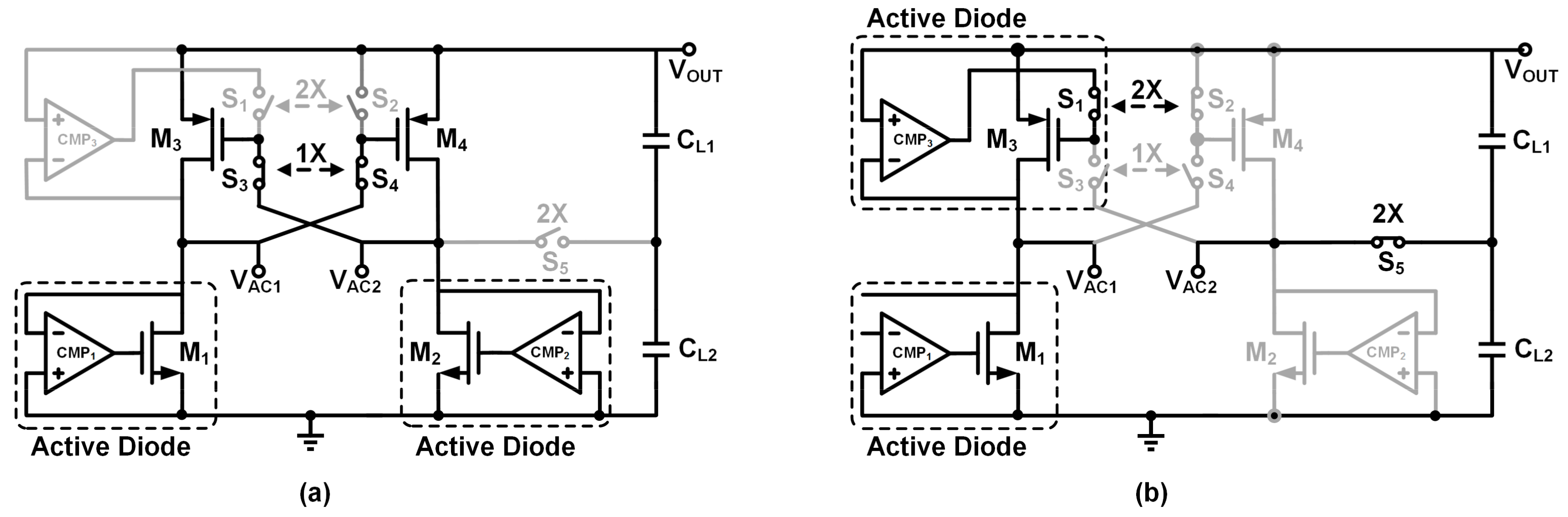
Figure 13.
(a) The block diagram of the reconfigurable resonant regulating (R3) rectifier; (b) the PWM regulation principle; and (c) V1× and V2× versus load resistance, where the RLa is the breakeven value and at which V2× = V1× [24].
Figure 13.
(a) The block diagram of the reconfigurable resonant regulating (R3) rectifier; (b) the PWM regulation principle; and (c) V1× and V2× versus load resistance, where the RLa is the breakeven value and at which V2× = V1× [24].

Figure 14.
The three-mode R3 rectifier configured as (a) a full-bridge rectifier (1× mode); (b) a half-bridge rectifier (½× mode); and (c) freewheeling (0× mode) [25].
Figure 14.
The three-mode R3 rectifier configured as (a) a full-bridge rectifier (1× mode); (b) a half-bridge rectifier (½× mode); and (c) freewheeling (0× mode) [25].

Figure 15.
(a) The block diagram of the switching-based current-mode (SCM) RX based on Q-modulation, which works at (b) the resonant phase and (c) the charging phase [28].
Figure 15.
(a) The block diagram of the switching-based current-mode (SCM) RX based on Q-modulation, which works at (b) the resonant phase and (c) the charging phase [28].

Figure 16.
The switching waveforms of (a) Q-modulation [28] and (b) multi-cycle Q-modulation (MCQ) [30]. Ctrl is on-off control signal of the switch S1.

Figure 17.
The block diagram of TX regulation is based on (a) supply voltage control [24] and (b) Vrefl control [32] for extending the regulation range. PA, power amplifier.

Figure 18.
The schematic of a class-D PA.

Figure 19.
TX regulation based on resonant frequency control, which is achieved with a weighted-capacitor array [34].
Figure 19.
TX regulation based on resonant frequency control, which is achieved with a weighted-capacitor array [34].

Figure 20.
The block diagram for subharmonic resonant switching [35]. EA, error amplifier.
Figure 20.
The block diagram for subharmonic resonant switching [35]. EA, error amplifier.


Figure 22.
The PA VPA and ITX waveforms when fsw = (a) fres/5 and (b) fres/4 by averaging out fres/3 and fres/5 [36].
Figure 22.
The PA VPA and ITX waveforms when fsw = (a) fres/5 and (b) fres/4 by averaging out fres/3 and fres/5 [36].

Figure 23.
(a) The schematic of TX regulation using PDM based on On-Off Keying (OOK) modulation, and (b) the waveforms of S1, S2, VG1~4, and VPA [37].
Figure 23.
(a) The schematic of TX regulation using PDM based on On-Off Keying (OOK) modulation, and (b) the waveforms of S1, S2, VG1~4, and VPA [37].

Figure 24.
(a) The schematic of TX regulation using the PDM based on ΔΣ-modulation, and the waveform of VPA when (b) d = 1 and (c) d = 0.5 [38]. P, positive; N, negative.
Figure 24.
(a) The schematic of TX regulation using the PDM based on ΔΣ-modulation, and the waveform of VPA when (b) d = 1 and (c) d = 0.5 [38]. P, positive; N, negative.
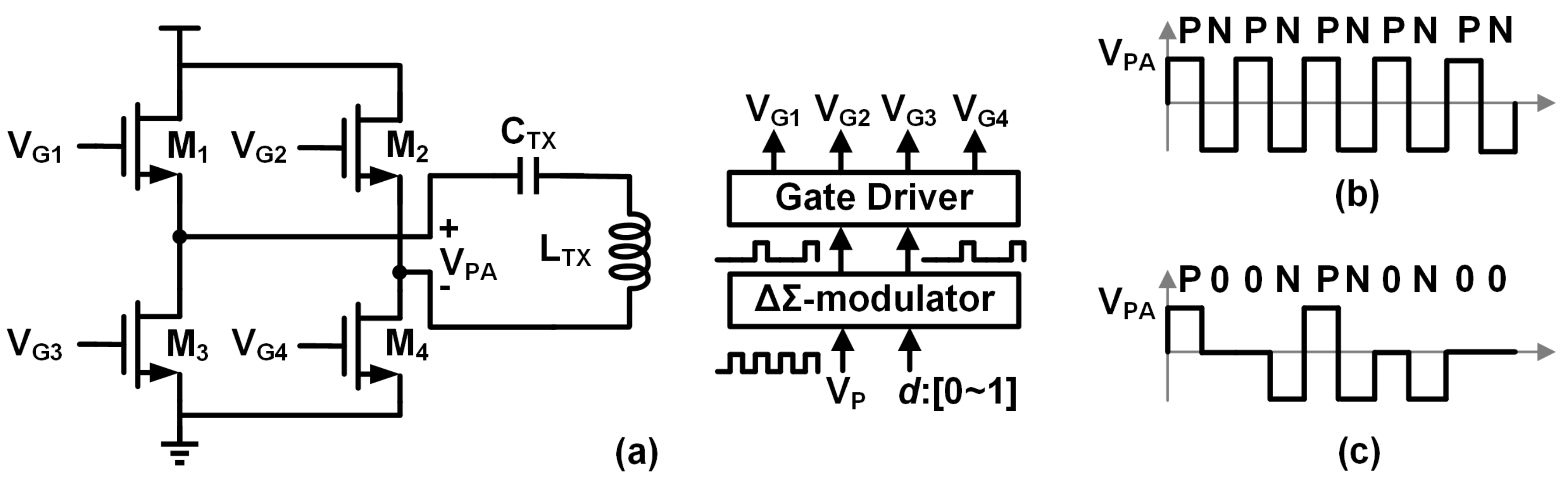
Figure 25.
The waveforms of VG1~4, VPA, and ITX in phase-shifted modulation (PSM), where α is the phase-shifted angle [39].
Figure 25.
The waveforms of VG1~4, VPA, and ITX in phase-shifted modulation (PSM), where α is the phase-shifted angle [39].

Figure 26.
(a) The schematic of the differential PA and (b) the waveforms of VG1-4, VPA, and ITX in harmonic-based phase-shifted modulation (HPSM) with the 3rd harmonic [40].
Figure 26.
(a) The schematic of the differential PA and (b) the waveforms of VG1-4, VPA, and ITX in harmonic-based phase-shifted modulation (HPSM) with the 3rd harmonic [40].
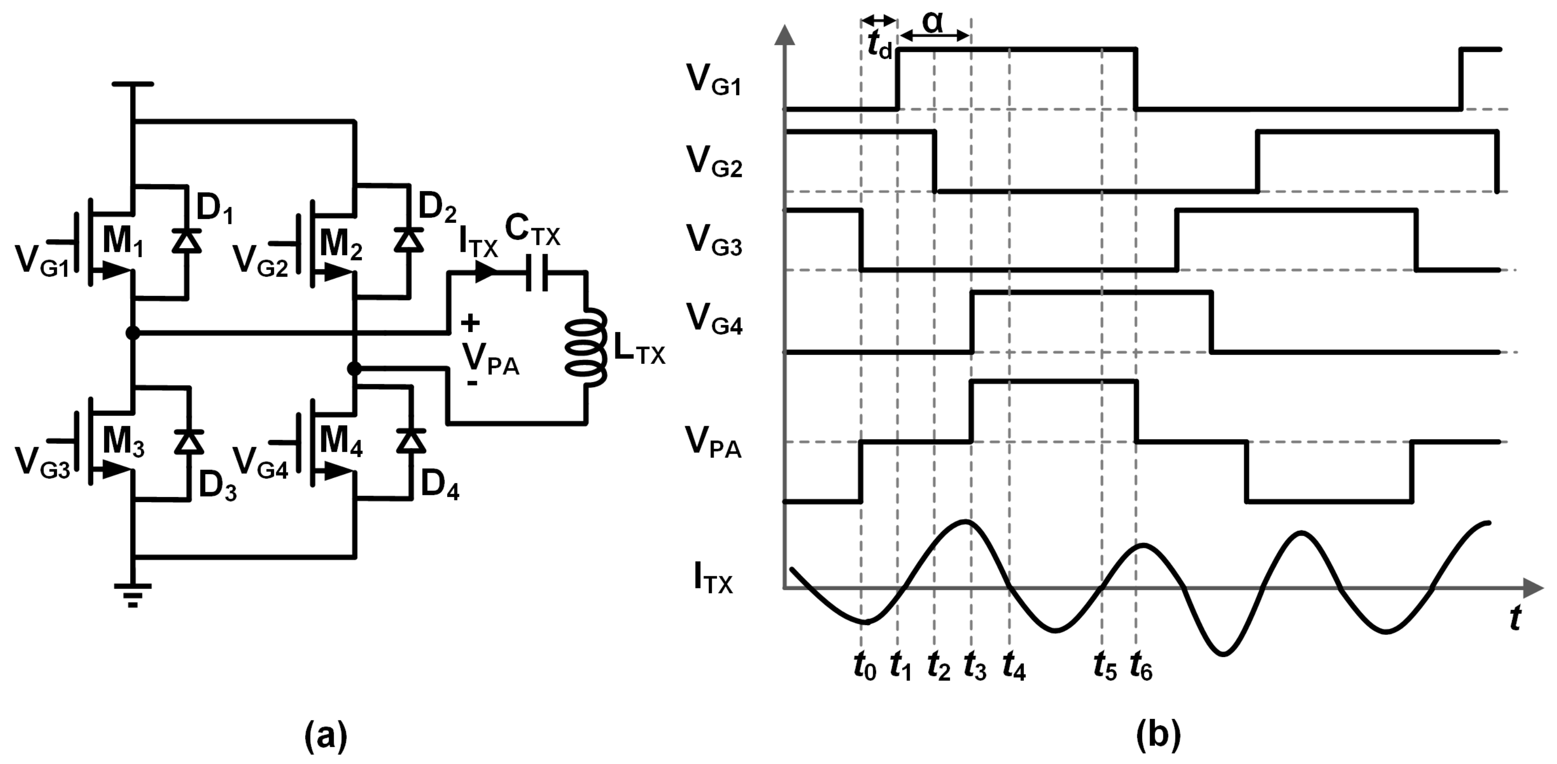
Figure 27.
TX regulation based on the vector power summing control technique [41,42], where the output power is summed over two vector-transmitted powers. DLL, delay locked loop; EA, error amplifier.

Table 1.
The comparison of RX regulation topologies in state-of-the-art R-WPT systems.
| References | [12] | [16] | [17] | [21] | [22] | [23] | [24] | [25] | [28] | [31] |
|---|---|---|---|---|---|---|---|---|---|---|
| Topology | Post-stage regulation | One-stage regulation | ||||||||
| Max. PDL | 40 mW | 6 W | 6 W | 0.7 mW | 12.8 mW | 2.68 W | 0.1 W | 6 W | 1.45 W | 96 μW # |
| Max. Rectifier Eff. | 85% | 92.8% | 92.5% # | Rectifier efficiency = PCE for one-stage regulation | ||||||
| Max. PCE | 74.8% | 84.6% | 86% | 60% | 87% | 96% | 92.6% | 92.2% | 87.1% | N/A |
| Max. PTE | N/A | N/A | 55% | N/A | N/A | 47.2% | 50% | N/A | ~46% # | 5.3% |
| Max. VCE | N/A | N/A | N/A | 0.92 | 0.92 | N/A | N/A | ~0.9 # | 0.82 # | 3.1 |
# Calculated from figures in the paper. PDL, power delivered to the load; PCE, power conversion efficiency; PTE, power transmission efficiency; VCE, voltage conversion efficiency.
Table 2.
The comparison of TX regulation topologies in the state-of-the-art R-WPT systems.
| References | [32] | [33] | [34] | [35] | [37] | [39] | [40] | [41] | [42] |
|---|---|---|---|---|---|---|---|---|---|
| Topology | Supply voltage control | fres control | PA power switch duty cycle control | Vector power summing control | |||||
| Max. PDL | 234 mW | 250 mW | 15 W | 0.52 W | 23.2 W | N/A | N/A | 1 W | 1 W |
| Max.PA Eff. | N/A | N/A | 80% | N/A | N/A | 94.5% | N/A | N/A | N/A |
| Max. PTE | 62.4% | 65.8% | N/A | 50% | 72.6% | N/A | 63.94% | 50% | 61.8% |
| Num. of TX | 1 | 2 | |||||||
© 2018 by the authors. Licensee MDPI, Basel, Switzerland. This article is an open access article distributed under the terms and conditions of the Creative Commons Attribution (CC BY) license (http://creativecommons.org/licenses/by/4.0/).
Share and Cite
MDPI and ACS Style
Liu, Y.; Li, B.; Huang, M.; Chen, Z.; Zhang, X. An Overview of Regulation Topologies in Resonant Wireless Power Transfer Systems for Consumer Electronics or Bio-Implants. Energies 2018, 11, 1737. https://doi.org/10.3390/en11071737
AMA Style
Liu Y, Li B, Huang M, Chen Z, Zhang X. An Overview of Regulation Topologies in Resonant Wireless Power Transfer Systems for Consumer Electronics or Bio-Implants. Energies. 2018; 11(7):1737. https://doi.org/10.3390/en11071737
Chicago/Turabian StyleLiu, Yang, Bin Li, Mo Huang, Zhijian Chen, and Xiuyin Zhang. 2018. "An Overview of Regulation Topologies in Resonant Wireless Power Transfer Systems for Consumer Electronics or Bio-Implants" Energies 11, no. 7: 1737. https://doi.org/10.3390/en11071737
Note that from the first issue of 2016, this journal uses article numbers instead of page numbers. See further details here.