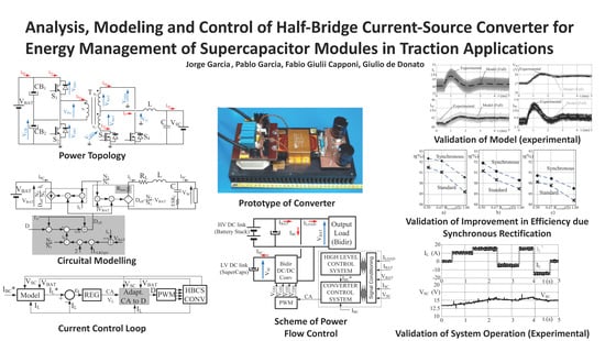
Article

Analysis, Modeling, and Control of Half-Bridge Current-Source Converter for Energy Management of Supercapacitor Modules in Traction Applications

1
LEMUR Group, Department of Electrical Engineering, University of Oviedo, 33204 Gijon, Spain
2
Department of Astronautical, Electrical and Energy Engineering, University of Roma “La Sapienza”, 00184 Roma, Italy
*
Author to whom correspondence should be addressed.
Energies 2018, 11(9), 2239; https://doi.org/10.3390/en11092239
Submission received: 13 July 2018 / Revised: 19 August 2018 / Accepted: 21 August 2018 / Published: 26 August 2018
(This article belongs to the Special Issue Design and Control of Power Converters 2019)

Abstract

:
In this work, an in-depth investigation was performed on the properties of the half-bridge current-source (HBCS) bidirectional direct current (DC)-to-DC converter, used to interface two DC-link voltage sources with a high-voltage-rating mismatch. The intended implementation is particularly suitable for the interfacing of a supercapacitor (SC) module and a battery stack in a hybrid storage system (HSS) for automotive applications. It is demonstrated that the use of a synchronous rectification (SR) modulation scheme benefits both the power-stage performance (in terms of efficiency and reliability) and the control-stage performance (in terms of simplicity and versatility). Furthermore, an average model of the converter, valid for every operating condition, is derived and utilized as a tool for the design of the control system. This model includes the effects of parasitic elements (mainly the leakage inductance of the transformer) and of the converter snubbers. A 3 kW prototype of the converter was used for experimental validation of the converter modeling, design, and performance. Finally, a discussion on the control strategy of the converter operation is included.

Graphical Abstract

1. Introduction

Among electrical energy storage passive devices, Supercapacitors (SC) outstand as one of the preferred solutions when very high power densities and long life cycles are required. These features also are used in Hybrid Storage Systems (HSS), where SC can be combined with other distinct storage devices, such as electrochemical batteries or fuel cells [1,2,3,4,5,6,7,8,9,10,11,12,13,14,15,16,17,18,19]. In these hybrid systems, SC usually operate as power sources, as they provide the required peak power commanded by the load. In turn, the combined device (e.g., the electrochemical battery) work as an energy source, providing the long-term energy required for the given operating conditions, such as islanding operation or back-up energy support after a fault ride-through sequence, etc.
The integration of SC into HSS has been covered extensively in the current state-of-the-art, by analyzing the modeling and operation of power electronic topologies, by proposing control algorithms and methods, and by investigating hierarchical energy management systems [20,21,22,23,24,25,26,27]. Although being the simplest and most inexpensive scheme, the direct connection between the storage systems prevents to fully exploit the high charging and discharging instant power ratings of SCs. This scheme also prevents a tight control on the independent power flows shared among the energy storage devices [28,29]. Therefore, practically every implemented solution found in the technical literature includes a bidirectional direct current (DC)-to-DC converter. These solutions can be categorized into three different classes: a series connection of the storage devices [6,7], a cascaded connection of the storage subsystems [8,9], and finally a parallel connection of the storage elements [10,11,12]. From a detailed analysis of the technical literature, the parallel configuration, depicted in 
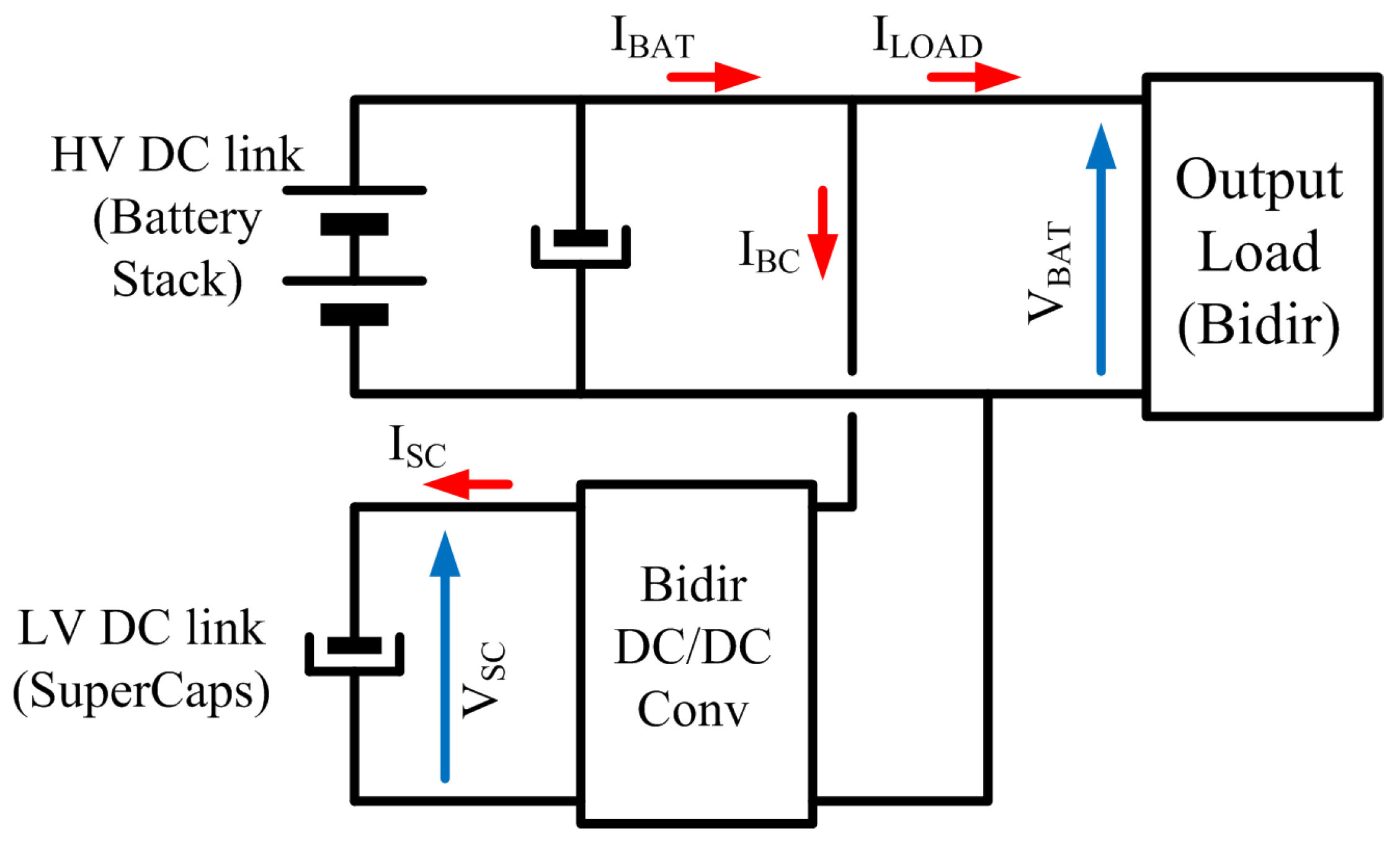
Figure 1, outstands as the most practical solution that allows a full control of the power flow sharing scheme required for the application, as well as a complete SC voltage-range utilization, despite that in this case the bidirectional converter needs to be rated for the peak value of the required power [13,14].
The bidirectional boost converter is formed by the typical connection present in a single phase leg of an inverter. It has two transistors, a series inductor connected between the mid-point of the transistors and the output, plus two capacitors intended to filter the input and the output of the converter. This scheme is generally adopted as the simplest and best-known solution. With this configuration, the peak power ratings required by most applications can be ensured by an assembly of few SC connected in series. This structure is also beneficial in terms of balancing the voltage at each SC module in the assembly. As a consequence, the SC side voltage ratings of the converter are usually much smaller than the voltage levels found at the DC-link. In addition, upon transient variations, the SC side voltage must allow variations from 80 to 20% of the SC ratings, in order to use efficiently the stored energy at the device. On the other side, the voltage at the DC-link may remain almost constant, as to optimize the full system design and operation. Hence, the range of the voltage gain between the input and the output of the bidirectional converter can typically surpass ratios of 1 to 10 and above, depending on the application.
Therefore, the boost converter is no longer a suitable solution, and so alternative topologies that allow for a high voltage gain need to be analyzed. Among these options, the most widely used include the use of a High-Frequency (HF) transformer [30,31,32,33,34,35,36,37,38]. Studies on the simplest isolated configurations, such as the bidirectional versions of the Flyback converter, the Forward Current-Source converter, the Push-Pull Current-Source converter, and the Half-Bridge Current-Source (HBCS) converter have been carried out [33,34,35]. These comparative analyses were carried out on the basis of the number of components, the switch stresses at the converters, and other figures of merit such as the utilization factor of the magnetic elements. This comparison shows how the bidirectional HBCS DC-to-DC converter is most suitable in low to medium power applications, for structures that directly interface the storage devices. Thus, the HBCS topology is of interest in HSS with storage devices arranged as shown in Figure 1 with the battery directly forming the DC bus at the converter. This is particularly interesting in traction applications, for which the weight and size of the full system are major concerns, and variable DC-link systems are considered as a suitable option [28,29].
When a given power profile is demanded by the load, the SC converter must react very quickly, in order to prevent the battery from providing the transient power. Given the current-source behavior of the low-voltage side of the HBCS converter, and provided that a tight, fast current control is implemented by generating the adequate SC current reference, the power delivered by this converter can successfully protect the battery from delivering fast, high power peaks, thus enhancing the performance and increasing the reliability of the full system. Other works have investigated the potential use of power converters for interfacing both the battery and the SC module, leading to more complex topologies and control methods [20,24,27,39].
The HBCS topology was introduced in an application to HSS in [11], but the power ratings of the laboratory demonstrator was only 100 W. Later, a 3 kW setup was reported in [35], being able to operate in open-loop, steady-state, both charging and discharging operation modes. A measured efficiency beyond 90% was then reported for the full range of operation. The authors in [35] analyzed the static gain of the HBCS converter, using conventioal switching patterns. Furthermore, they considered neither the modeling nor the control stage for closed-loop operation of the converter. On the other hand, the authors of [40,41] showed preliminary research conducted to unify the transfer function of the converter acting in a bidirectional operation scheme, as well as the dynamic behavior.
The present work investigates more in depth the performance of the HBCS converter in vehicle applications. Firstly, a unified control strategy of the converter, on the basis of a synchronous rectification switching pattern, is provided. By using this pattern, the converter can be controlled with a simple, unique control law valid for every operating condition. This allows the implementation of a full bidirectional SC current control, thus enabling a fast, tight power flow control in the storage system. Once this switching pattern is established and validated, the main contribution of this work is the extension of previously existing circuital models of the converter by including non-ideal effects of the parasitic elements in the transformer of the converter, as well as the dissipative effect of the losses in the system. The performance of the proposed model was validated through simulations and experiments carried out on a 3 kW laboratory prototype. The proposed model was also compared against the simplified ideal model. Finally, this work discusses the control strategy that can be implemented in the converter. A basic HBCS current loop was analyzed, designed, and implemented, with the aim to demonstrate its feasibility; finally, a discussion on the possibilities of the high-level control strategy is also included at the end of the paper.
This paper is organized as follows. Section 2 presents the conventional modulation strategy implemented in the state-of-the-art for the HBCS converter. After that, Section 3 evaluates the Synchronous Rectification (SR) scheme in the converter operation, considering both the charging and discharging modes of operation. It also demonstrates experimentally the benefits of SR operation for this topology. Section 4 further discusses the implications of SR in terms of the simplification of the control of the converter; most importantly, this section provides an averaged model of the HBCS converter, suitable to aid in the design of the control stage. Also, this model is validated through simulations. Subsequently, in Section 5 the current control algorithm is discussed and tested through simulations. This section also deals with the overall control scheme of the system. Section 6 validates the full model and the control scheme outlined in the previous sections by showing experimental results obtained with a laboratory prototype of a HBCS converter. Finally, Section 7 discusses the conclusions of the research and proposes some future developments.

2. Special Characteristics of the HBCS Converter

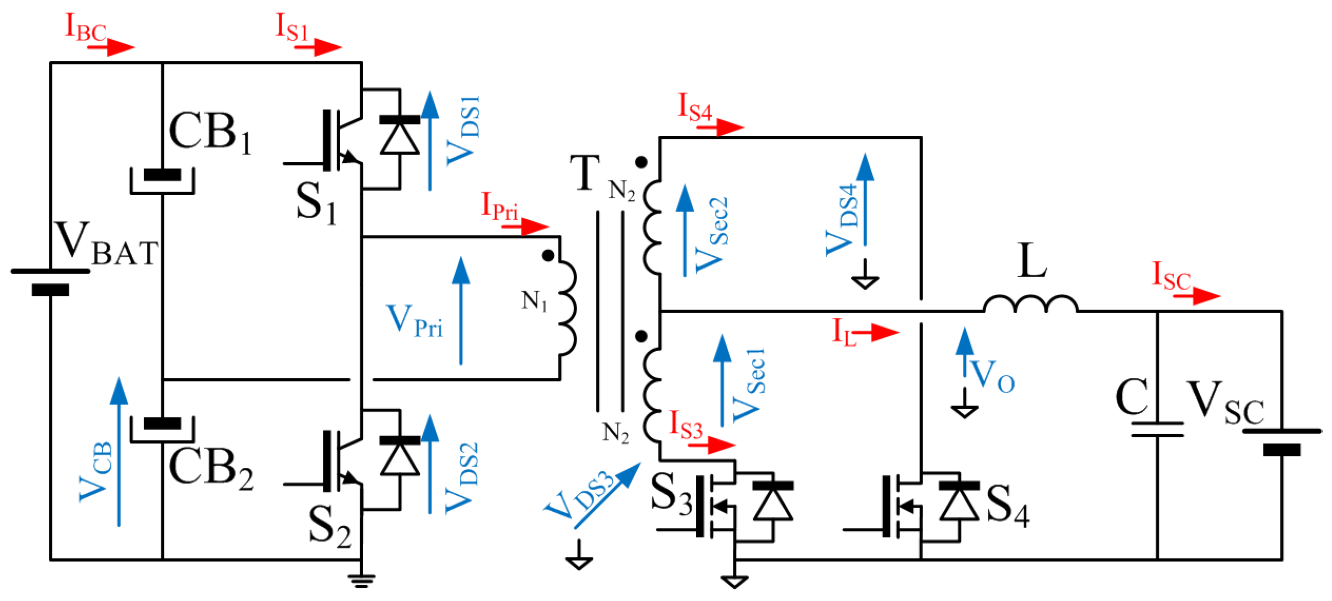
Figure 2 shows the HBCS converter. Because this converter is a bidirectional topology, no predefined input or output are established. For the coming discussion, the SC side is also referred to as the Low-Voltage (LV) side, signifying that this side generally has the lower of the rated voltages involved in the analysis. On the other hand, the alternate energy source (i.e., battery) and the DC-link are referred to as the High-Voltage (HV) side.
The modulation scheme for the HBCS converter, as presented in [35], is obtained by shifting the command pulse waveforms of each switch in the primary- or secondary-side by 180°. Initially, the control parameters implemented at both charging and discharging operation modes were different. In charging mode, where the energy flows to the SC from the DC link side, switches S 3 and S 4 remain always turned off. This forces the current to flow only through the diodes of S 3 and S 4 . 
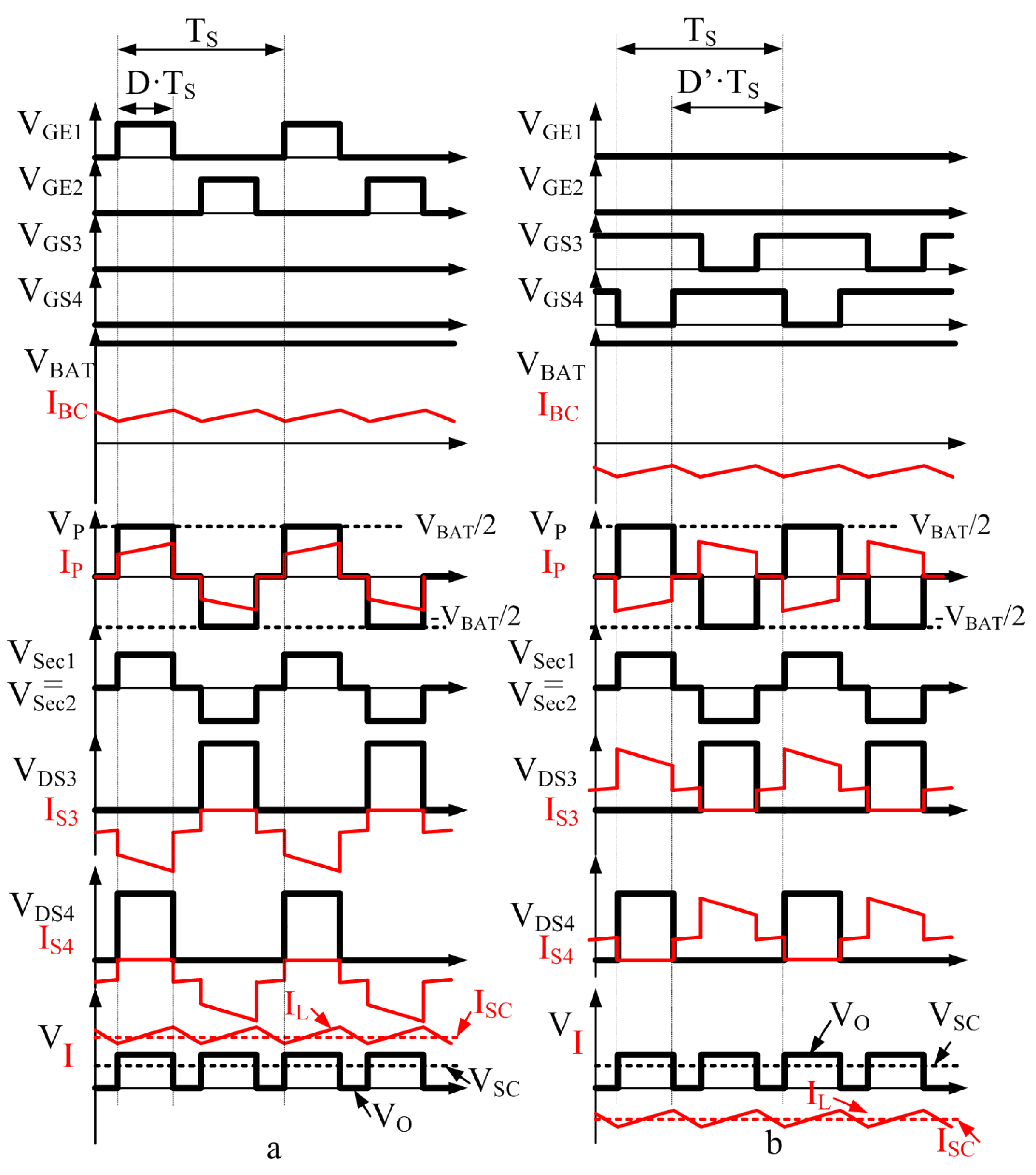
Figure 3 shows the main current and voltage instant waveforms of the converter for charging (a) and discharging (b) modes. The switching pattern is defined by establishing the gate-to-emitter voltages of switches S 1 to S 4 , denoted as V G E 1 V G E 4 , respectively. The rest of the waveforms are consistent with the references in Figure 2. The modulation of switches S 1 and S 2 (Figure 3a) is carried out by shifting by 180° the control pulses, considering a given duty ratio, D:
D = T S 1 O N T S ,
where T S 1 O N is the interval when switch S 1 remains turned on and T S is the switching period. In order to avoid a simultaneous conduction of switches S 1 and S 2 at the battery side, and given that the switching pattern requires a fixed 180 phase shift between the firing signals of V G E 1 and V G E 2 , D is restricted to 0 < D < 0.5 . The voltage gain between the LV and HV sides, G C H R G E , is
G C H R G E = V S C V B A T = D · N 2 N 1 ,
where N 1 and N 2 are the primary- and secondary-side number of turns of the HF transformer, respectively; V S C is the voltage across the SC; and V B A T is the DC-link voltage, that is, the battery voltage according to its state of charge. The magnetizing inductance of the transformer is neglected, because it is assumed that it is very high.
Figure 4 shows the current paths for the different switching modes of the converter, during the SC charging operation scheme. When switch S 1 is turned on and S 2 is turned off (Figure 4a), a positive current I P flows flows through the primary side, considering the references in Figure 2. Current flows through the portion of the secondary winding connected to switch S 3 , the output filter, and the SC; thus, the anti-parallel diode of switch S 3 carries the secondary-side current. Figure 4b, in turn, shows the switching mode when both transistors S 1 and S 2 are turned off. The inductor current I L splits equally between the two parts of the secondary winding, flowing through the anti-parallel diodes of S 3 and S 4 . Finally, Figure 4c depicts the current paths when S 2 is turned on and S 1 is turned off. This mode is similar to that shown in Figure 4a but considers the 180 phase shift between S 1 and S 2 .
During the discharging mode, the energy flows back to the DC-link from the the SC. In this case, the switches under control are S 3 and S 4 , while S 1 and S 2 are kept continuously turned off. Again, the modulation of S 3 and S 4 is implemented through a 180° shifting scheme, while the turn-on intervals are kept equal. Figure 3b shows the key waveforms obtained for this operation mode. The independent parameter for this mode, D , is defined as:
D = T S 3 O N T S ,
where T S 3 O N is the interval when S 3 is turned on. The constraint for this parameter is now 0.5 < D < 1 , thus forcing an overlap in the conduction of S 3 and S 4 . This overlapping is required because of the current-source behavior of the LV side of the converter. For this topology, unless at least one switch in the pair S 3 S 4 is turned on, an abrupt interruption of the current flowing through the inductor would lead to a dangerous overvoltage across the magnetic element, that might damage the converter. For the discharging operation mode, the voltage gain can be defined as:
G D I S C H R G E = V B A T V S C = 1 1 D N 1 N 2 .
The switching modes for discharging the SC are represented in Figure 5. The current path when S 4 is turned off and S 3 is turned on is shown in Figure 5a. On the other hand, Figure 5b shows the current flowing through the switches when both S 3 and S 4 are turned on. Finally, it can be seen in Figure 5c how the current flows when switch S 4 is turned on and S 3 remains off. A close look at Figure 5a–c shows that the current paths are the same as those shown in Figure 4a–c, respectively, but with the directions of the currents reversed.
By using the control laws stated in Equations (2) and (4), both the charging and discharging control strategies can be easily designed. However, this modulation pattern requires the calculation of two independent control parameters, defined as the duty cycles of S 1 and S 3 , depending on the operation mode under consideration, given by charging and discharging modes, respectively. This approach, though, yields to some issues at the boundary between these operation modes, given that the switches that must be controlled change abruptly. Therefore, if both control schemes are implemented independently, a smooth transition between modes of operation is prevented. However, this issue is easily avoided provided that SR is implemented. This SR pattern is introduced in the next section for the HBCS converter. The benefits for the control of the converter are discussed in the forthcoming sections.

3. Synchronous Rectification in the HBCS Converter

SR is a common strategy that establishes a given switching pattern for the switches in power electronic converters. Upon several conditions, it can decrease conduction losses, thus boosting the efficiency of the converter. This technique has already been described in the technical literature related with hybrid systems applications [36,37,38]. This technique takes advantage of the low on-state voltage of a MOSFET transistor, when compared to the forward voltage of its body diode. Given the equivalent series circuit of a diode, formed by a threshold voltage, V T H , and a dynamic resistor, R D Y N , then the conduction losses, for the diode turned on, are given by:
P C D I O D E V T H · I D + R D Y N · I D 2 .
Moreover, the conduction losses in a MOSFET can be expressed as:
P C M O S F E T R D S O N · I D 2 ,
where R D S O N is the drain-to-source on-resistance of the channel. As a result of an analysis of the equivalent circuit of the switch, the current tends to flow through the path with a lower voltage drop. In the HBCS converter depicted at Figure 2, S 3 and S 4 have already been implemented as MOSFET switches, with inherent anti-parallel body diodes. As a consequence, SR can be directly applied.
In order to validate the performance of the SR switching pattern, a reference design is considered for a 3 kW HBCS converter. The main characteristics of the setup are detailed in Table 1.
Figure 6 shows a graphical representation of the expression of the drain-to-source voltage, V D S , as well as the power dissipated through conduction losses, P C O N D , both as a function of the current flowing through the drain of the transistor, I D . These power and voltage values are given for both the transistor and diode elementary devices. For this study, the actual values given in the datasheets of the real components selected, in this case the S K M 121 A R power MOSFET modules from SEMIKRON, have been used. The dotted black line shows the voltage at the MOSFET as a function of the current I D . This line shows the typical load line of a resistive component. As a consequence, the power dissipated as a function of the I D in the MOSFET is given by a quadratic relationship expressed in Equation (6), drawn as a filled black line in Figure 6. The voltage drop across the diode, in turn, is shown as an horizontal dotted gray line. The power dissipated in the diode, as a function of the current I D , therefore follows a linear behavior, represented by a filled gray line. As can be seen, both power characteristics, those of the MOSFET and the diode, have an intersection point labeled as I L I M . For I D current values below I L I M , the MOSFET losses are smaller than the diode losses, and therefore the synchronous rectification implies higher efficiencies compared to the standard switching pattern. For the real values of the devices under consideration, I L I M is equal to
I L I M = 70 A .
From Table 1, the maximum value of the SC current, which is also the maximum currents allowed to flow through S 3 and S 4 , has a value of 65 A. Therefore, and considering Figure 6, the conduction losses at the secondary side of the converter operating in charging mode will be decreased, provided that SR is implemented as the switching pattern. As a consequence, the whole efficiency of the converter will increase. It must be notice that in this case the switches at the DC link side have been implemented by means of IGBT switches. Therefore, and given that for this switch technology the current flowing from the emitter to the collector can only flow through the anti-parallel diode (and not through the transistor itself, as in the previous case), the use of a SR scheme during the SC discharge mode will not mean a decrease in the converter losses. In any case, a critical point for this analysis is to state that SR can still be used in this mode of operation without affecting the performance of the converter. This issue will be discussed in Section 4.
A first set of experiments was carried to validate the feasibility of the SR switching pattern implementation in the HBCS converter. For this validation, and in order to register the steady-state operation of the converter, the setup was configured to supply a resistive load from a voltage source. The values of measured efficiencies in charging operation mode, for the standard and the SR schemes, are given in Figure 7. Three different resistive loads (1.0, 0.67 and 0.5 Ω , respectively), were used in the measurements. The voltage at the power source was kept constant at 300 V D C . Due some practical constraints at the experimental setup, the voltage levels at the LV side were limited to three values, V S C = 25 V, V S C = 30 V, and V S C = 34 V. From the plots at Figure 7, it can be deduced an increase in the converter efficiency in all cases.

4. Full Model of the Converter under Synchronous Rectification

As a result of the use of SR, the HV and LV side switches, S 1 S 2 and S 3 S 4 , present complementary control signals. In particular, the gating signals of S 3 and S 4 , are the complementary signals of S 1 and S 2 , respectively, as it was sketched in the waveforms shown in Figure 3a,b. This condition defines an obvious relationship upon SR scheme between the values of the parameter D of switches S 1 S 2 and D of switches S 3 S 4 . This can be expressed as
D = 1 D .
As a result, a single, independent control parameter can be established for every operation mode in the converter, given that the remaining parameters are calculated automatically. This parameter is the duty ratio of switch S 1 , noted by D. Equation (8), together with Equations (2) and (4), determines a unique equation to define the voltage gain of the topology, G H B C S . This equation is, as mentioned, true for every mode of operation and charging condition:
G H B C S = V S C V B A T = D · N 2 N 1 .
Thus, with SR, the control law turns out to be unique, regardless of the mode of operation.
Once the switching strategy is defined, an accurate model of the converter needs to be established in order to properly design the control system. The simplest averaged large-signal model for the converter is shown in Figure 8. This basic model has already been explored in the definition and implementation of a control strategy for the topology [40]. The basic model has been implemented considering ideal switching and reactive devices. For the average circuit, the transistors and the HF transformer have been modeled by the two dependent sources within the dashed frames at Figure 8. The output value of these sources depend on the duty ratio D and on the turns ratio of the transformer, N 2 / N 1 . Downstream from these, the second order LC filter is present.
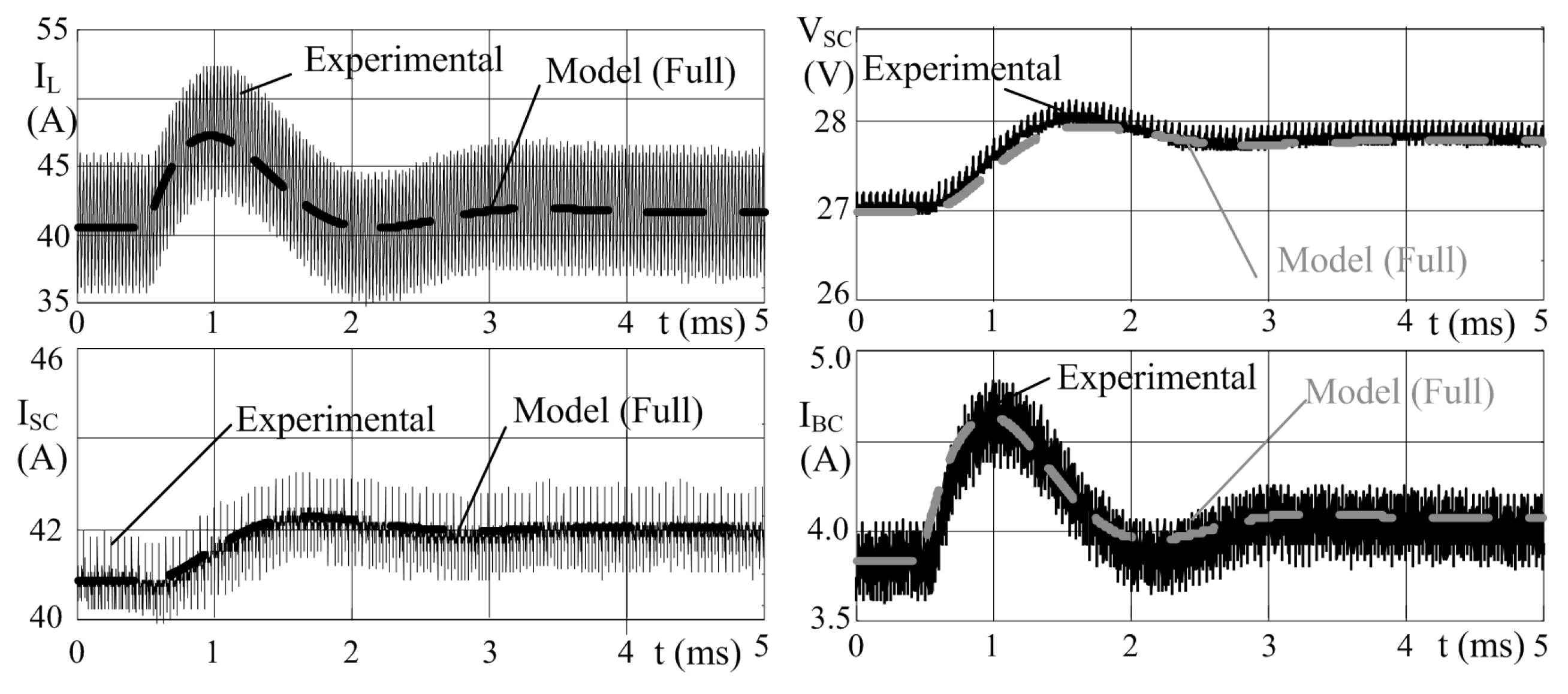
In order to check this model, the performance of the circuit depicted in Figure 8 was compared with a full switching model of the HBCS converter, implemented in PSIM. In these simulations, a resistive load replaced the SCs, with the aim of having initial steady-state operation conditions. The dynamic behavior is obtained by imposing a small step in the duty ratio of the converter after reaching the steady state. In the tests shown in Figure 9, the step goes from 0.34 to 0.36. This picture shows the simulated waveforms of the output voltage ( V S C ), input ( I B C ) and output ( I S C ) currents, and the inductor current ( I L ), compared with their corresponding averaged values obtained from the basic model. The performance of the basic model differs significantly from the switching converter behavior. Even thought the natural frequency is mainly the same, there are two effects of mismatch in the behavior of the model. Firstly, the switching system is more damped than the dynamic response given by the model. Moreover, the equilibrium values after the transient are smaller in the switching circuit.
In order to solve this disagreement between the model and the switching circuit, an improved model has been developed. This model firstly accounts for the effects of the parasitic resistors of the transformer, the R D S of the transistors at the HV side, and the snubbers. These effects are jointly modeled by a series resistance, R l o s s , which adds a dissipative term in the model that contributes to increase the damping factor. However, the most significant effect is due to the leakage inductance of the transformer, depicted in Figure 10. Some waveforms are depicted in Figure 11 to describe the contribution of this leakage inductance in the full model. For simplicity in this analysis, the overall primary side leakage inductance is obtained as the sum of the measured primary- and reflected measured secondary-side leakage inductances.
The waveform sequence starts when S 1 and S 2 are turned off, and thus there is no current flowing through the primary side of the transformer. In this situation, the output inductor current splits equally through the diodes at switches S 3 and S 4 . At time t 0 , S 1 is turned on, forcing the primary side voltage, V P , to be half the voltage across the battery:
V P = V B A T 2 .
The high inductance of the filter, L, causes I L to keep flowing practically unchanged to the load. For the ideal transformer in Figure 11a, the current immediately flows through S 1 , and thus the diodes of S 3 and S 4 are instantly turned-off. As a consequence, the secondary side voltages at the transformer instantly are equal to:
V S e c 1 = V S e c 2 = V B A T 2 N 2 N 1 .
Nonetheless, for the real transformer case depicted in Figure 10, the leakage inductance prevents the secondary side current to change instantly (Figure 11b). Upon this situation current keeps flowing through the secondary sides of the transformer, S 3 and S 4 . The secondary side voltages remain null immediately after turning on S 1 , and thus the voltage at the leakage inductor equals the primary-side voltage. This issue affects the operation of the system. For instance, in charging mode, both HV-side switches, S 1 and S 2 , are in the off-state just before S 1 is turned on. It can be seen in Figure 2 and Figure 3a that each diode at the secondary side carries half I L , while the voltages at the primary side, V P , and at the common node of the secondary windings, V O , are null:
I S 3 = I S 4 = I L ( t ) 2 = I L 2 ,
V 0 = 0 ,
V P = 0 .
Equation (12) describes as well that the inductor current is considered as constant within a switching interval. When S 1 turns on at t 0 , and given that current keeps on flowing through the LV side diodes, then the voltage V P does not vary. Instead, because V D S 1 equals zero, the voltage at the primary side of the real transformer (i.e., considering the parasitic inductance), V P R , equals half the voltage at the battery:
V P R = V B A T 2 .
Therefore, the values of the voltage across the leakage inductor, V L k , and the current at the primary side of the transformer, I L k , can be calculated as:
V L k = V B A T 2 ,
I L k = I P R = 1 L L k V B A T 2 · t .
As mentioned previously, the overall leakage inductance L L k takes into account the measured leakage inductor at the primary ( L L k P r i ) and secondary ( L L k S e c ) sides of the real transformer, referred to the primary side:
L L k = L L k P r i + L L k S e c 2 N 1 N 2 2 .
Upon these conditions, the inductance L L k is linearly charged. The currents through S 3 and S 4 are given by:
I S 3 = I L 2 I P R 2 N 1 N 2 ,
I S 4 = I L 2 + I P R 2 N 1 N 2 .
At instant t 1 , I S 4 is null, turning S 4 off, and thus from this instant the current I L equals the current through the body diode of S 3 :
I S 3 = I L ,
I S 4 = 0 .
As a consequence, the dead time t d , defined as the interval between instants t 0 and t 1 ,
t d = t 1 t 0
is the time it takes for the current I S 3 to reach I L after S 1 is turned on. This condition can be expressed as:
I L 2 1 2 N 1 N 2 V B A T 2 1 L L k ( t 1 t 0 ) = I L ( t ) .
The explicit expression for t d can thus be obtained:
t d = 2 · N 2 N 1 I L ( t ) V B A T · L L k .
It is important to note that t d represents a completely different behavior in the full model when compared to the basic one. For the basic model, when switch S 1 is turned on, V O equals to half the battery voltage, obviously referred to the secondary side. Instead, for the full model, V O is zero during t d just after turning S 1 on, and then reaches the same V B A T / 2 for the rest of the interval when S 1 remains turned on. This situation affects the final voltage gain at the topology, given that the effective duty ratio of the converter, D e f f , is actually smaller for the full model than for the basic one. This D e f f can be defined now as:
D e f f = D 1 · T S t d T S .
As it can be deduced from Equation (25), the expression of the dead time is a non-linear function of a manifold of system parameters. Hence, the resulting model that takes this t d into account is a non-linear model. The large-signal circuital model that considers t d (and also R l o s s ) is shown in Figure 12. Additionally, the Equivalent Series Resistor, E S R C , of the filter capacitor C has been included.
The full average model has been simulated and compared with the switching circuit, in order to evaluate its performance. These simulations, shown in Figure 13, have been carried out in the same conditions that were established for the previous simulations of the basic model shown in Figure 9. It can be seen how the new complete model tracks much more accurately the simulated waveforms at the switching model, again for a duty step from 0.34 to 0.36. Therefore it can be concluded that the dynamic behavior of the HBCS converter with the proposed SR scheme is truly represented by the obtained full model.
An important remark on this behavior ir that this response corresponds to a second order system, as it is expected from a resistive load at the output of the LC filter at the LV side. In the proposed application, the load is an assembly of SC. If this assembly is considered as an ideal pure capacitive load, given that the capacitance value of these devices is very large, then the output voltage would remain constant during the transient, and thus the dynamic behavior of the output voltage can be disregarded. For a more realistic approach, the SC assembly will be modeled by an equivalent circuit formed by a series resistor and the SC capacitor. Still, the SC will present a very large capacitance value, and therefore it behaves practically as a DC voltage source. Thus, the AC small signal model of the SC is given by the series resistor only, and the behavior of the full system is again corresponding to a second order system.
At this point, a small-signal model can be derived. Figure 14 shows the model that emerges after linearizing and perturbing the large signal full model, which has the following parameters:
R 1 = t d T S
R 2 = 2 · D · L L k P r i T S N 2 N 1 2
K 1 = N 2 N 1 · I L 1 t d T S
K 2 = 2 · t d T S · D · N 2 N 1
K 3 = N 2 N 1 · V B A T 2 · I L 2 · L L k P r i T S N 2 N 1 2
This last model finally allows the design and tuning of the control system, since the most significant dynamics of the system are taken into account. The second order behavior of the system, represented in the previous analysis, can be also derived from this model. In fact, the output voltage to duty ratio transfer function, can be calculated as:
v ^ S C d ^ v ^ B A T = 0 = K 3 · R 0 R 0 + E S R C · 1 + s · C · E S R C R E Q + R 0 R 0 + E S R C + s · L R 0 + E S R C + C · R E Q + R 0 · E S R C R 0 + E S R C + s 2 · L · C
where
R E Q = R 2 + R l o s s + R L

5. Proposed Control Scheme for the HBCS Converter

An adequate design of the control stage of the converter is needed in order to ensure the required power flows in the hybrid storage system under consideration [20,21,22,23,24,25,26,27,28,29]. In order to obtain the desired operating performance of the system, a High Level Control System provides the instant power references that each storage device must supply to the DC link. From this power reference, the HV current value of the HBCS converter, I B C * can be calculated. This scheme is depicted in Figure 15 [40].
Considering that the final control parameter is the inductor current, I L , the converter control stage covers two different aspects: Firstly, it is required that this stage generates a reference for such current, I L * , starting from the HV side current, I B C * . In addition, it implements a feedback control loop for such inductor current.

5.1. Feedback Control Loop for the SC current

This inductor current control loop is shown in Figure 16a. It must be noticed how the average value of I L equals the average value of I S C . In order to design and tune the regulator, the inductor voltage to inductor current transfer function G ( s ) can be defined as:
G ( s ) = 1 R L + s · L
For the current loop, a standard PI regulator has been designed. This regulator is tuned using the zero-pole cancellation method, and setting the desired bandwidth of the current loop. The regulator consists of a pure integrator and a zero that cancels the pole given by the inductance L and the ESR of the filter inductor, R L . This ensures that the final bandwidth of the controlled system can be designed to a target value. The characteristic frequency of this zero might change upon eventual variations of the equivalent series resistor due temperature excursions, ageing, or even manufacturing tolerances. However, assuming an adequate design of this inductor filter, then the ESR of this magnetic element will be relatively small; therefore, the variations in this parameter will not significantly affect the final performance of the controlled system. Once the regulator is tuned, the final implementation needs to obtain the expression of the duty ratio, D, from the control action of the current loop, C A . Considering Equations (25) and (26) and Figure 12, the relationship between D and V L can be calculated:
V L = D e f f · N 2 N 1 · V B A T V S C = D · 1 t d T S N 2 N 1 · V B A T V S C .
Finally,
D = N 1 N 2 · V L + V S C V b a t N 2 N 1 · 2 · I L · L L k P r i T S .
Figure 16b shows the implemented control scheme. The shaded box implements Equation (36), obtaining the duty ratio D from the control action of the current loop, C A , which is V L . Figure 17 shows simulations of the performance of this inner loop for a bandwidth of 500 Hz. This plot provides a sequence of current steps as a reference to the current loop, I L * . It can be seen how the actual current value tracks perfectly the reference. Moreover, the current can swiftly change its direction, changing automatically from charging to discharging operation modes, even for large relative current steps. This feature is a consequence of using the discussed SR modulation scheme in the topology.

5.2. Generation of the SC Current Reference

The complete control scheme is shown in Figure 18. An external estimator stage is designed to generate the feedback loop current reference, I L * , from the original I B C * reference. The relationship between the HV-side current and the inductor current can be obtained from the model in Figure 14 as
i ^ B C = K 1 · d ^ + 1 R 1 · v ^ B A T + N 2 N 1 · D K 2 · i ^ L ,
i ^ B C i ^ L d ^ = 0 v ^ B A T = 0 = N 2 N 1 · D K 2 .
The value of the inductor current reference, I L * , is estimated from the HV-side current, I B C * , by means of the model, as is given in Equation (38). Other control strategies based on additional feedback loops, such as a cascaded control loop to generate the inductor current reference, would imply a more complex implementation of the controller, in terms of computation, number of sensors, filtering and signal conditioning stages, and so on. In addition, they would provide a decrease in the dynamics, given that the external loop dynamics requires a bandwidth significantly smaller than that of the inner loop, in order to ensure a good overall performance.

6. Experimental Results

Figure 19 shows a 3 kW laboratory prototype of the HBCS, used in this work for the practical demonstration of the system performance. The main characteristics of the setup are detailed in Table 1. Preliminary results of the performance of this setup were reported in [35].
Figure 20 shows the experimental waveform of the converter, with the same operating conditions as reported in Figure 9. It can be seen how the experimental waveforms were very similar to the simulated waveforms for the switching converter. It also can be seen how the ideal model failed to track the real waveforms properly.
Similarly, Figure 21 compares the proposed complete model, including the effects of the parasitic leakage inductance of the transformer and the resistance to account for the losses, against the experimental waveforms, resembling the conditions stated for Figure 13. This validates the obtained model for the HBCS converter, as the complete model tracked the real converter waveforms very accurately.
In order to validate experimentally the implementation of the control scheme, a series of current reference steps were implemented in the converter. The reference steps that were provided to the simulations, shown in Figure 17, were also supplied to the laboratory prototype. Figure 22 shows the performance of the experimental setup. It can be seen how the real converter performed as expected, thus validating the converter control scheme.
In order to check the dynamics of the inner control loop, a detailed experimental response of one of such current steps is shown in Figure 23.

7. Conclusions and Future Developments

This research has demonstrated the feasibility of the HBCS converter as a bidirectional power converter for HSS systems in traction applications, where the DC-link is directly connected to the battery bank. The main topics covered include the analysis and design of the power and control stages, the modeling including parasitic elements of the topology, and a validation procedure through a laboratory prototype.
As a first contribution, it has been demonstrated that the use of SR is a suitable switching scheme in the converter, given the demonstrated benefits in the efficiency and the enhancement in the control system implementation. By means of this switching pattern, a full, bidirectional power flow control can be simply implemented in the converter. Moreover, this feature is obtained at no cost, since the required hardware elements to implement SR pattern are present in the conventional HBCS topology.
Another key contribution is to include the parasitic elements in the topology aiming to obtain a highly representative circuital model of the converter. This model has been demonstrated by means of simulations and through experiments in a 3 kW laboratory setup. With the information derived from this dynamic model, the design of the control stage for the HSS can be easily implemented. This research also has provided a design example of a current control loop in order to govern the power flow in the HSS outlined.
A series of future developments arise from this research. One of these developments is the implementation of the HSS in a full powertrain for vehicle applications, including the integration of the HBCS converter control with the complete high-level control system. Another development covers the optimization of the converter power topology and control system, including the definition of the control strategy for the complete system. Additionally, the extension of the application of the HBCS converter to other types of loads (e.g., inductive loads) can be considered in future research.

Author Contributions

J.G. and F.G.C. conceived the research and designed and performed the experiments; all the authors analyzed the data and contributed to the discussion and conclusions.

Funding

This work has been partially supported by the Innovation Development and Research Office (MEC), Spanish Government, under Research Grants ENE2013-44245-R, Project “Microholo” and ENE2016-77919, Project “Conciliator”, and by the European Union through ERFD Structural Funds (FEDER). This work has been co-funded by the Campus of International Excellence (CEI) of the University of Oviedo, Spain, as a Mobility Grant for Academics in 2013, partially funded by the Gijon City Hall, by resolution of BOPA 156, 6-VII-2013.

Conflicts of Interest

The authors declare no conflict of interest.

Abbreviations

The following abbreviations are used in this manuscript:
CAControl action
DCDirect current
ESREquivalent series resistor
LVLow-voltage
HBCSHalf-bridge current-source
HFHigh-frequency
HSSHybrid storage system
HVHigh-voltage
IGBTInsulated-gate bipolar transistor
MOSFETMetal-oxide-semiconductor field-effect transistor
SCSupercapacitor
SRSynchronous rectification

References

  1. Ostadi, A.; Kazerani, M.; Chen, S.K. Hybrid Energy Storage System (HESS) in vehicular applications: A review on interfacing battery and ultra-capacitor units. In Proceedings of the 2013 IEEE Transportation Electrification Conference and Expo (ITEC), Detroit, MI, USA, 16–19 June 2013; pp. 1–7. [Google Scholar]
  2. Amjadi, Z.; Williamson, S.S. Digital Control of a Bidirectional DC/DC Switched Capacitor Converter for Hybrid Electric Vehicle Energy Storage System Applications. IEEE Trans. Smart Grid 2014, 5, 158–166. [Google Scholar] [CrossRef]
  3. Kuperman, A.; Mellincovsky, M.; Lerman, C.; Aharon, I.; Reichbach, N.; Geula, G.; Nakash, R. Supercapacitor Sizing Based on Desired Power and Energy Performance. IEEE Trans. Power Electron. 2014, 29, 5399–5405. [Google Scholar] [CrossRef]
  4. Cohen, I.J.; Kelley, J.P.; Wetz, D.A.; Heinzel, J. Evaluation of a Hybrid Energy Storage Module for Pulsed Power Applications. IEEE Trans. Plasma Sci. 2014, 42, 2948–2955. [Google Scholar] [CrossRef]
  5. Farooque, M.; Maru, H.C. Fuel cells-the clean and efficient power generators. Proc. IEEE 2001, 89, 1819–1829. [Google Scholar] [CrossRef]
  6. Di Napoli, A.; Caricchi, F.; Crescimbini, F. Fuel cells-the clean and efficient power generators. In Proceedings of the 6th European Conference on Power Electronics, Seville, Spain, 19–21 September 1995. [Google Scholar]
  7. Mestre, P.; Astier, S. Application of supercapacitors and influence of the drive control strategies on the performances of on electric vehicle. In Proceedings of the 15th Electric Vehicle Symposium (EVS-15), Bruxelles, Belgium, 29 September–3 October 1998. [Google Scholar]
  8. Grbovic, P.J.; Delarue, P.; Moigne, P.L.; Bartholomeus, P. Modeling and Control of the Ultracapacitor-Based Regenerative Controlled Electric Drives. IEEE Trans. Ind. Electron. 2011, 58, 3471–3484. [Google Scholar] [CrossRef]
  9. Schmidt, M. EV Mini-Van Featuring Series Conjunction of Ultracapacitors and Batteries for Load Leveling of its Batteries. In Proceedings of the 15th Electric Vehicle Symposium (EVS-15), Bruxelles, Belgium, 29 September–3 October 1998. [Google Scholar]
  10. Itani, K.; Bernardinis, A.D.; Khatir, Z.; Jammal, A.; Oueidat, M. Regenerative Braking Modeling, Control, and Simulation of a Hybrid Energy Storage System for an Electric Vehicle in Extreme Conditions. IEEE Trans. Transp. Electr. 2016, 2, 465–479. [Google Scholar] [CrossRef]
  11. King, R.; Schwartz, J.; Cardinal, M.; Garrigan, K. Development and system test of high efficiency ultracapacitor/battery electronic interface. In Proceedings of the 15th Electric Vehicle Symposium (EVS-15), Bruxelles, Belgium, 29 September–3 October 1998. [Google Scholar]
  12. Di Napoli, A.; Crescimbini, F.; Solero, L.; Caricchi, F.; Giulii Capponi, F. Multiple-input DC-DC power converter for power-flow management in hybrid vehicles. In Proceedings of the Conference Record of the 2002 IEEE Industry Applications Conference, 37th IAS Annual Meeting (Cat. No.02CH37344), Pittsburgh, PA, USA, 13–18 October 2002; Volume 3, pp. 1578–1585. [Google Scholar]
  13. Di Napoli, A.; Giulii Capponi, F.; Solero, L. Power Converter Arrangements with Ultracapacitor Tank for Battery Load Leveling in EV Motor Drives. In Proceedings of the 8th European Conference on Power Electronics, Lausanne, Switzerland, 7–9 September 1999. [Google Scholar]
  14. Herath, N.; Binduhewa, P.; Samaranayake, L.; Ekanayake, J.; Longo, S. Design of a dual energy storage power converter for a small electric vehicle. In Proceedings of the 2017 IEEE International Conference on Industrial and Information Systems (ICIIS), Peradeniya, Sri Lanka, 15–16 December 2017; pp. 1–6. [Google Scholar]
  15. Kouchachvili, L.; Yaïci, W.; Entchev, E. Hybrid battery/supercapacitor energy storage system for the electric vehicles. J. Power Sources 2018, 374, 237–248. [Google Scholar] [CrossRef]
  16. Song, Z.; Li, J.; Hou, J.; Hofmann, H.; Ouyang, M.; Du, J. The battery-supercapacitor hybrid energy storage system in electric vehicle applications: A case study. Energy 2018, 154, 433–441. [Google Scholar] [CrossRef]
  17. Cabrane, Z.; Ouassaid, M.; Maaroufi, M. Analysis and evaluation of battery-supercapacitor hybrid energy storage system for photovoltaic installation. Int. J. Hydrogen Energy 2016, 41, 20897–20907. [Google Scholar] [CrossRef]
  18. Hernández, J.; Sanchez-Sutil, F.; Vidal, P.; Rus-Casas, C. Primary frequency control and dynamic grid support for vehicle-to-grid in transmission systems. Int. J. Electr. Power Energy Syst. 2018, 100, 152–166. [Google Scholar] [CrossRef]
  19. Thounthong, P.; Piegari, L.; Pierfederici, S.; Davat, B. Nonlinear intelligent DC grid stabilization for fuel cell vehicle applications with a supercapacitor storage device. Int. J. Electr. Power Energy Syst. 2015, 64, 723–733. [Google Scholar] [CrossRef]
  20. Sun, L.; Feng, K.; Chapman, C.; Zhang, N. An Adaptive Power-Split Strategy for Battery-Supercapacitor Powertrain-Design, Simulation, and Experiment. IEEE Trans. Power Electron. 2017, 32, 9364–9375. [Google Scholar] [CrossRef]
  21. Bougrine, M.; Benalia, A.; Delaleau, E.; Benbouzid, M. Minimum time current controller design for two-interleaved bidirectional converter: Application to hybrid fuel cell/supercapacitor vehicles. Int. J. Hydrogen Energy 2018, 43, 11593–11605. [Google Scholar] [CrossRef]
  22. He, H.W.; Xiong, R.; Chang, Y.H. Dynamic Modeling and Simulation on a Hybrid Power System for Electric Vehicle Applications. Energies 2010, 3, 1821–1830. [Google Scholar] [CrossRef] [Green Version]
  23. Shah, N.; Czarkowski, D. Supercapacitors in Tandem with Batteries to Prolong the Range of UGV Systems. Electronics 2018, 7, 6. [Google Scholar] [CrossRef]
  24. Zhang, Q.; Deng, W. An Adaptive Energy Management System for Electric Vehicles Based on Driving Cycle Identification and Wavelet Transform. Energies 2016, 9, 341. [Google Scholar] [CrossRef]
  25. Passalacqua, M.; Lanzarotto, D.; Repetto, M.; Marchesoni, M. Advantages of Using Supercapacitors and Silicon Carbide on Hybrid Vehicle Series Architecture. Energies 2017, 10, 920. [Google Scholar] [CrossRef]
  26. Wang, Y.; Hu, H.; Zhang, L.; Zhang, N.; Sun, X. Real-Time Vehicle Energy Management System Based on Optimized Distribution of Electrical Load Power. Appl. Sci. 2016, 6, 285. [Google Scholar] [CrossRef]
  27. Wang, B.; Xu, J.; Wai, R.J.; Cao, B. Adaptive Sliding-Mode With Hysteresis Control Strategy for Simple Multimode Hybrid Energy Storage System in Electric Vehicles. IEEE Trans. Ind. Electron. 2017, 64, 1404–1414. [Google Scholar] [CrossRef]
  28. Thounthong, P.; Rael, S. The benefits of hybridization. IEEE Ind. Electron. Mag. 2009, 3, 25–37. [Google Scholar] [CrossRef]
  29. Lai, J.; Nelson, D.J. Energy Management Power Converters in Hybrid Electric and Fuel Cell Vehicles. Proc. IEEE 2007, 95, 766–777. [Google Scholar] [CrossRef]
  30. Trovão, J.P.; Silva, M.A.; Dubois, M.R. Coupled energy management algorithm for MESS in urban EV. IET Electr. Syst. Transp. 2017, 7, 125–134. [Google Scholar] [CrossRef]
  31. Jain, M.; Daniele, M.; Jain, P.K. A bidirectional DC-DC converter topology for low power application. IEEE Trans. Power Electron. 2000, 15, 595–606. [Google Scholar] [CrossRef]
  32. Kazimierczuk, M.K.; Vuong, D.Q.; Nguyen, B.T.; Weimer, J.A. Topologies of bidirectional PWM dc-dc power converters. In Proceedings of the IEEE 1993 National Aerospace and Electronics Conference-NAECON 1993, Dayton, OH, USA, 24–28 May 1993; Volume 1, pp. 435–441. [Google Scholar]
  33. Giulii Capponi, F.; Cacciato, F. Using Super Capacitors in Combination with Bi-Directional DC/DC Converters for Active Load Management in Residential Fuel Cell Applications. In Proceedings of the 1st European Symposium on Supercapacitors (ESSCAP’04), Belfort, France, 4–5 November 2004. [Google Scholar]
  34. Cacciato, M.; Caricchi, F.; Giulii Capponi, F.; Santini, E. A critical evaluation and design of bi-directional DC/DC converters for super-capacitors interfacing in fuel cell applications. In Proceedings of the Conference Record of the 2004 IEEE Industry Applications Conference, 39th IAS Annual Meeting, Seattle, WA, USA, 3–7 October 2004; Volume 2, pp. 1127–1133. [Google Scholar]
  35. Giulii Capponi, F.; Santoro, P.; Crescenzi, E. HBCS Converter: A Bidirectional DC/DC Converter for Optimal Power Flow Regulation in Supercapacitor Applications. In Proceedings of the 2007 IEEE Industry Applications Annual Meeting, New Orleans, LA, USA, 23–27 September 2007; pp. 2009–2015. [Google Scholar]
  36. Zhang, Y.; Guo, Z.; Zhang, Y.; Zhan, T.; Jin, L. Active battery/ultracapacitor hybrid energy storage system based on soft-switching bidirectional converter. In Proceedings of the 2013 International Conference on Electrical Machines and Systems (ICEMS), Busan, South Korea, 26–29 October 2013; pp. 2177–2182. [Google Scholar]
  37. Wai, R.J.; Duan, R.Y. High-Efficiency Bidirectional Converter for Power Sources with Great Voltage Diversity. IEEE Trans. Power Electron. 2007, 22, 1986–1996. [Google Scholar] [CrossRef]
  38. Yamamoto, K.; Hiraki, E.; Tanaka, T.; Nakaoka, M.; Mishima, T. Bidirectional DC-DC converter with full-bridge/push-pull circuit for automobile electric power systems. In Proceedings of the 2006 37th IEEE Power Electronics Specialists Conference, Jeju, South Korea, 18–22 June 2006; pp. 1–5. [Google Scholar]
  39. Dusmez, S.; Hasanzadeh, A.; Khaligh, A. Comparative Analysis of Bidirectional Three-Level DC DC Converter for Automotive Applications. IEEE Trans. Ind. Electron. 2015, 62, 3305–3315. [Google Scholar] [CrossRef]
  40. Garcia, J.; Giulii Capponi, F.; Borocci, G.; Garcia, P. Control strategy for Bidirectional HBCS Converter for supercapacitor applications. In Proceedings of the 2014 IEEE 23rd International Symposium on Industrial Electronics (ISIE), Istanbul, Turkey, 1–4 June 2014; pp. 1794–1799. [Google Scholar]
  41. Garcia, J.; Garcia, P.; Giulii Capponi, F.; Borocci, G.; De Donato, G. Analysis, modeling and control of half-bridge current-source converter for supercapacitor applications. In Proceedings of the 2014 IEEE Energy Conversion Congress and Exposition (ECCE), Pittsburgh, PA, USA, 14–18 September 2014; pp. 3786–3793. [Google Scholar]
Figure 1. Parallel configuration for interfacing supercapacitors (SCs) with primary energy source (battery stack).
Energies 11 02239 g001
Figure 2. Layout of Half-Bridge Current-Source (HBCS) bidirectional converter. The references for the current and voltage considered for the analysis are shown.
Energies 11 02239 g002
Figure 3. Main voltage (black) and current (red) waveforms of the half-bridge current-source (HBSC) for charging (a) and discharging (b) operation modes.
Energies 11 02239 g003
Figure 4. Switching modes of the half-bridge current-source (HBCS) converter operating during supercapacitor (SC) charging operation mode. (a) Switch S 1 on and switch S 2 off. (b) Both switches S 1 and S 2 off. (c) Switch S 1 off and switch S 2 on.
Energies 11 02239 g004
Figure 5. Switching modes of the half-bridge current-source (HBCS) converter operating during supercapacitor (SC) discharging operation mode. (a) Switch S 3 on and switch S 4 off. (b) Both switches S 3 and S 4 turned on. (c) Switch S 3 off and switch S 4 on.
Energies 11 02239 g005
Figure 6. Drain-to-source voltage ( V D S , dashed lines) and conduction losses ( P C O N D , filled lines) for both diode conduction (gray) and MOSFET conduction (black), for the half-bridge current-source (HBCS) prototype.
Energies 11 02239 g006
Figure 7. Graphical relationship of experimental efficiency measurements between standard and synchronous rectification switching schemes, as a function of load resistance. (a) V S C = 25 V. (b) V S C = 30 V. (c) V S C = 34 V.
Energies 11 02239 g007
Figure 8. Large-signal averaged model based on ideal components.
Energies 11 02239 g008
Figure 9. Simulation waveforms (gray) and averaged value of model based on ideal components (black), for filter current ( I L ), load output current ( I S C ), load voltage ( V S C ), and input current ( I B C ).
Energies 11 02239 g009
Figure 10. Half-bridge current-source (HBCS) converter equivalent circuit, including the overall leakage inductor at the primary side of the transformer.
Energies 11 02239 g010
Figure 11. (a) Switching waveforms with ideal transformer. (b) Switching waveforms with overall leakage inductor at the primary side.
Energies 11 02239 g011
Figure 12. Full averaged large-signal model based on real components, parasitic elements, and snubbers.
Energies 11 02239 g012
Figure 13. Simulation waveforms (gray) and averaged value of model based on the parameters of real components (black), for filter current ( I L ), load output current ( I S C ), load voltage ( V S C ) and input current ( I B C ).
Energies 11 02239 g013
Figure 14. Full Small Signal Model of the system.
Energies 11 02239 g014
Figure 15. Control Strategy for the HBCS converter.
Energies 11 02239 g015
Figure 16. Inner control loop approach (a) for designing and tuning the regulator and (b) for implementing the control scheme.
Energies 11 02239 g016
Figure 17. Simulation of inductor current I L (gray, upper plot) and supercapacitor (SC) voltage V S C (black, lower plot) during step changes in the commanded current (black, lower plot). Positive current corresponds to charging mode, negative to discharging mode.
Energies 11 02239 g017
Figure 18. Complete control scheme for the half-bridge current-source (HBCS) converter.
Energies 11 02239 g018
Figure 19. Laboratory prototype of the half-bridge current-source (HBCS) converter.
Energies 11 02239 g019
Figure 20. Experimental waveforms (gray) and averaged value of model based on ideal components (black, dashed), for filter current ( I L ), load output current ( I S C ), load voltage ( V S C ), and input current ( I B C ).
Energies 11 02239 g020
Figure 21. Experimental waveforms (gray) and averaged value of model based on real components (black), for filter current ( I L ), load output current ( I S C ), load voltage ( V S C ), and input current ( I B C ).
Energies 11 02239 g021
Figure 22. Inductor current I L (black, upper plot) and supercapacitor (SC) voltage V S C (black, lower plot) during step changes in the commanded current I L * (referenced by dashed gray lines). Positive current corresponds to charging mode, negative to discharging mode.
Energies 11 02239 g022
Figure 23. Inductor current I L (black) and reference I L * (grey) during one step change.
Energies 11 02239 g023
Table 1. Characteristics of half-bridge current-source (HBCS) design.
ParameterMax.Min.
SC voltage45 V25 V
HV DC-link voltage350 V
Switching frequency20 kHz
SC discharge-mode duty ratio0.750.55
SC charge-mode duty ratio0.450.25
Output power (SC disch. mode)3 kW1.6 kW
Output power (SC chrg mode)3 kW1.6 kW
SC current65 A−65 A
Transformer turns ratio3.5:1:1

