DC Offset Error Compensation Algorithm for PR Current Control of a Single-Phase Grid-Tied Inverter †

1
Department of Electrical Engineering, Chonbuk National University, Jeollabuk-do 54896, Korea
2
Department of Electrical Engineering, Kyungnam University, Changwon 51767, Korea
*
Author to whom correspondence should be addressed.
†
2017 IEEE Applied Power Electronics Conference and Exposition (APEC), Tempa, FL, USA, 26–30 March 2017.
Energies 2018, 11(9), 2308; https://doi.org/10.3390/en11092308
Submission received: 17 July 2018
/
Revised: 17 August 2018
/
Accepted: 27 August 2018
/
Published: 2 September 2018
(This article belongs to the Special Issue Power Electronics 2018)
Abstract
:In a single-phase grid-tied inverter, the direct current (DC) offset error included in the measured grid side phase current has various causes, such as a non-ideal current sensor, unbalanced power supply of an operational amplifier, and nonlinear features of analog components in interface circuits, etc. If the DC offset error is included in the measured current, it causes the secondary harmonic of fundamental frequency and the DC component in grid phase current which result in degradation of inverter performance. In this paper, a theoretical detection method of the secondary harmonic of the fundamental frequency and a DC component in grid phase current for a proportional-resonant (PR) current control system is introduced. Based on the detection method, an algorithm for compensating DC offset error is also presented for single-phase grid-tied inverters. Simulation results and experimental verification of the DC offset error compensation algorithm are shown in this paper.
1. Introduction
Recently, grid-tied inverters have received attention due to the high demands of distributed energy systems [1,2]. Among the grid-tied inverters, the single-phase grid-tied inverter has advantages over three-phase grid-tied inverter for low power applications because a transformer is not necessarily required. Reliable phase current control on the grid side is necessary for efficient operation of a single-phase grid-tied inverter. The phase current of the grid side is measured through the following process: (1) a current sensor; (2) analog signal processing circuits, and (3) analog-digital converter (ADC). During the measurement process of phase current, nonlinear characteristics result in a direct current (DC) offset error [3]. To prevent the DC current component, a line frequency isolation transformer was used in References [4,5], but it is applicable, typically, for three-phase inverters. As another approach, an offset error was detected using a reactor [6]. However, the use of a reactor requires additional hardware systems and size and weight of the overall hardware system is increased due to the reactors. Other DC offset compensation methods are presented in References [7,8,9,10]. However, the DC offset compensation methods result in additional cost and power losses. An algorithm-based DC offset compensation is proposed in Reference [11] where scaling error and DC offset in measured phase current are integrated over one cycle of a grid frequency, and information about the error is analyzed from the integrated signal. For the implementation of the method in Reference [11], integration of one cycle of phase current is required for error compensation. As a result, transient dynamic performance is reduced because of the one cycle delay.
There are many current control algorithms for a single-phase grid-tied inverter, for example, proportional-integral (PI) control at stationary and synchronous reference frames, resonant control, predictive control, repetitive control, etc. [12]. While PI control is simple to implement, PI control at a stationary reference frame yields phase delay which needs to be compensated. PI control at a synchronous reference frame shows a zero steady state error, but it has limited control performance for high harmonic order signals. Performance of current control can be improved via predictive control and repetitive control [13,14]. However, predictive control is sensitive to variations of parameters used to develop the control algorithm, and repetitive control shows slow dynamic performance. Along with PI control, a proportional-resonant (PR) control is one of the widely used control algorithms for a grid-tied inverter [15,16,17,18,19]. Linear quadratic tracking (LQT) is applied for resonant controller design [15,16]. A design guideline of a PR controller for a single-phase grid-tied inverter is presented in References [17,18]. In Reference [19], the reference frame of the current is transformed from phase A to a synchronous reference frame. Then, current ripple is caused by the DC offset error. A PR controller is used to obtain DC offset error information from the ripple component on a d-axis current. As introduced in Reference [19], gain tuning of a PR controller is challenging because PR control is sensitive to variation of the DC offset error magnitude. While presented methods proposed algorithms for removing DC offset error, causes of DC offset in a digital signal process have not been analyzed in detail yet.
In this paper, causes of DC offset error in a phase current measuring process and effects of DC offset error in measured phase current on a grid side are theoretically analyzed. Since the operating and signal processing conditions are different for each application, this paper is attempting to compensate the variable and unpredictable DC offset signal. As well as the analysis of DC offset error effect, a DC offset error rejection method is presented utilizing second order generalized integrator (SOGI), and different types of filters, such as low pass filter (LPF) and all pass filter (APF). The proposed method rejects the second harmonic and DC component caused by the DC offset error. Finally, the proposed method enables efficient and stable operation of a single-phase grid-tied inverter. Simulation and experimental results of the proposed algorithm are shown in this paper.
2. Analyzing Effect of DC Offset Error in PR Current Control
A system flow of a single-phase grid-tied inverter system is shown in Figure 1. The system shown includes a PR current controller, a DC-link voltage controller and a phase locked loop (PLL).
Figure 2 shows the measurement process of a phase current in a single-phase grid-tied system, where a DC offset error has occurred.
As seen in Figure 2, phase current of a grid-tied inverter is measured using a matching circuit, a current sensor, and analog components, for example, a low pass filter and analog to digital converter. A measured current signal contains both scaling and DC offset error when compared with an ideal current signal because of nonlinear features of the current measuring process as seen in Figure 2. Specifically, DC offset error occurs from a transducing process of current into voltage by a current sensor and transformation of the analog signal to digital values by Analog to Digital (A/D) converters [3]. Although scaling error occurs at multiple stages in a current measurement process as shown in Figure 2, scaling error is disregarded in this paper because a single-phase system is not affected by scaling error. Since this paper proposes a solution to the problem in a phase current control loop, it is assumed that DC-link voltage and phase information PLL as shown in Figure 1 are ideal.
Electrical circuit equations for measured phase voltage (vs), measured phase current (is) in a grid including DC current offset errors (Δioffset) which occurred during current measurement process are shown as Equations (1) and (2). The output power (Ps) equation can be derived by multiplying Equations (1) and (2) and is summarized as Equation (3). In addition, power on DC-link (Pdc) is written as Equation (4).
From Equation (1) to Equation (3), Vm and Im represent the magnitude of voltage and current, respectively. In Equation (4), Vdc and Idc represent voltage and current on DC-link, respectively. Assuming power on DC-link (Pdc) is equal to output power, the DC-link current can be derived as a form of DC-component (IDC) and ripple component (Iripple) as Equation (5).
where, and .
As seen in Equation (5), ripple current consists of a fundamental frequency component and the second harmonic component. The additional fundamental frequency component, , is generated due to the current offset (Δioffset). Using the ripple component in a DC-link current, DC-link voltage ripple (Vdc_ripple) due to the offset error can be derived as Equation (6).
As shown in Figure 1, current command () is calculated from a DC-link voltage controller, and the ripple also appears as an identical form in a DC-link voltage. Therefore, an output of a DC-voltage controller and a current command can be written as Equation (7).
As seen in Equation (7), a current command developed from a DC-link voltage controller contains three components, which are ideally the fundamental current command, a component due to double line frequency ripple generated from a grid side, and a current component generated by the DC offset error, Δioffset. Among components in the current command Equation (7), the current component () generated by the DC offset error (Δioffset) is written as Equation (8) disregarding the effect of scaling error.
From Equation (8), it is known that DC component, and second order harmonic signals, are generated in the current reference signal due to the offset error, Δioffset, in phase current. By removing the ripple component due to the DC offset error in a measured phase current, power quality of a single-phase grid-tied inverter can be improved. Using the DC offset error analysis result, a DC offset error compensation algorithm is developed to improve power quality of a grid system.
3. Proposed Offset Error Compensation Algorithm
The proposed DC offset error compensation algorithm is integrated into a current control system and graphically represented in Figure 3.
Figure 3 shows that measured phase current () is applied as an input signal of the proposed DC offset error compensation algorithm of a single-phase grid-tied inverter system. As shown in Equation (8), phase current () is affected by the DC offset error and contains the second harmonic component of a fundamental frequency. As the first step of the proposed DC offset error compensation algorithm, the second harmonic of the fundamental frequency occurring from a DC offset error in phase current is pulled out by using a SOGI. The transfer function of the SOGI is derived as Equation (9).
In Equation (9), s is a Laplace operator and kp is a proportional gain and k is a bandwidth gain, and ωr is a resonance frequency. By using the SOGI, a designated frequency signal can be selectively extracted from an input signal. The signal processing in Figure 3 is shown more in detail in Figure 4 and unity magnitude is applied to each signal. In Figure 4a, the fundamental frequency is assumed to be 60 Hz, and the fundamental frequency signal is plotted with a black line. The second harmonic signal extracted by the SOGI is plotted in blue in Figure 4a.
The second step is divided into two stages. The first stage is generating a virtual phase current with 90-degree phase lagging utilizing a feature of an APF. A transfer function of an APF is shown in Equation (10). Same as in Equation (9), s is a Laplace operator in Equation (10).
The 90-degree phase lagged signal generated by the APF is plotted in red dashed line in Figure 4a. The second stage of the second step is taking absolute values of second harmonic signal extracted from the SOGI and 90-degree phase lagged second harmonic signal generated from the APF. By taking absolute values of second harmonic signal, the frequency of the signal is double, which is a fourth order harmonic of the fundamental frequency signal as shown in plots in blue and red lines in Figure 4b. By adding a fourth order harmonic signal (blue line in Figure 4a) and 90-degree phase lagged fourth order signal (red dashed line in Figure 4a), an eighth harmonic signal is generated as shown in magenta Figure 4b. Therefore, a DC signal including a ripple with eighth order harmonics frequency occurs as an output signal of Step 2. The fundamental frequency signal (black line) is overlaid for frequency verification. Then, an estimated DC offset component () can be obtained by eliminating the eighth harmonic signal from the DC signal. In Step 3, an LPF is used to remove the eighth harmonic signal, and DC signal can be obtained. Since the obtained DC signal cannot be directly used as DC offset compensation, the obtained DC signal is used as a comparison signal of zero command PI controller as shown in Step 3 in Figure 3. Finally, the DC offset compensation component () is developed from the PI controller. The output signal of the PI controller compensates DC offset error of a grid phase current. By applying the proposed algorithm, the DC offset error (Δioffset) is estimated and directly eliminated from the measured phase current. As a result, the DC component and the second harmonic signal in Equation (8) can be removed by eliminating the DC offset error (Δioffset) from the measured phase current. Therefore, accurate DC offset error compensation in a single-phase grid-tied system is enabled using the proposed algorithm.
4. Simulation Results
A simulation model of the proposed DC offset error compensation algorithm was developed and implemented in MATLAB/Simulink (Mathworks, Natick, MA, USA). The developed simulation model is shown in Figure 5.
For performance verification of the proposed DC offset error compensation algorithm, 0.2 A of DC offset was injected intentionally. The simulation results with and without applying the proposed algorithm for DC offset error compensation are seen in Figure 6. Figure 6a,b show the DC-link voltage and phase current when the proposed DC offset compensation algorithm is not applied and Figure 6c,d show the DC-link voltage and phase current when the proposed DC offset compensation algorithm is applied, respectively.
As seen in Figure 6a,c, the DC offset error on measured phase current is compensated by applying the proposed algorithm. In Addition, the ripple on DC-link voltage due to the DC offset error is significantly reduced by applying the proposed algorithm as seen in Figure 6b,d. However, the harmonic components in DC-link voltage and phase current are not clearly shown in the simulation results at a time domain.
Therefore, in addition to analysis in a time domain, frequency spectrum of phase current was investigated, and simulation results with and without applying the proposed algorithm are shown in Figure 7, respectively. As shown in Figure 7a, the DC component and the second harmonic are observed in phase current as theoretically analyzed in Equation (8). As shown in Figure 7b, the DC offset component and the second harmonic component are almost completely removed by using the proposed the DC offset error compensation algorithm.
As well as DC offset error compensation, we investigated total harmonic distortion (THD) of the phase current and it improves from 2.79% to 0.41% when the proposed DC offset compensation algorithm is applied as shown in Figure 7.
5. Experimental Results
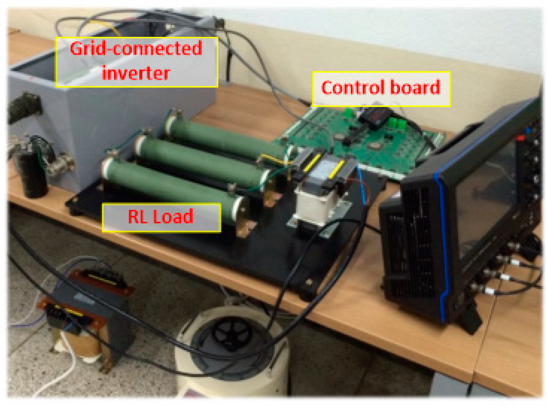
Following the simulation, the proposed algorithm was verified by experimental implementation. This section presents an experimental set-up and experimental results of the proposed DC offset error compensation algorithm. A block diagram of the experimental set-up and the picture of the experimental set-up are shown in Figure 8 and Figure 9.
In the experimental set-up, TMS320VC33 (TMS 320 series, Texas Instruments, Dallas, TX, USA) was used as a digital signal processor to design the control algorithms. More details about the experimental set-up are summarized in Table 1.
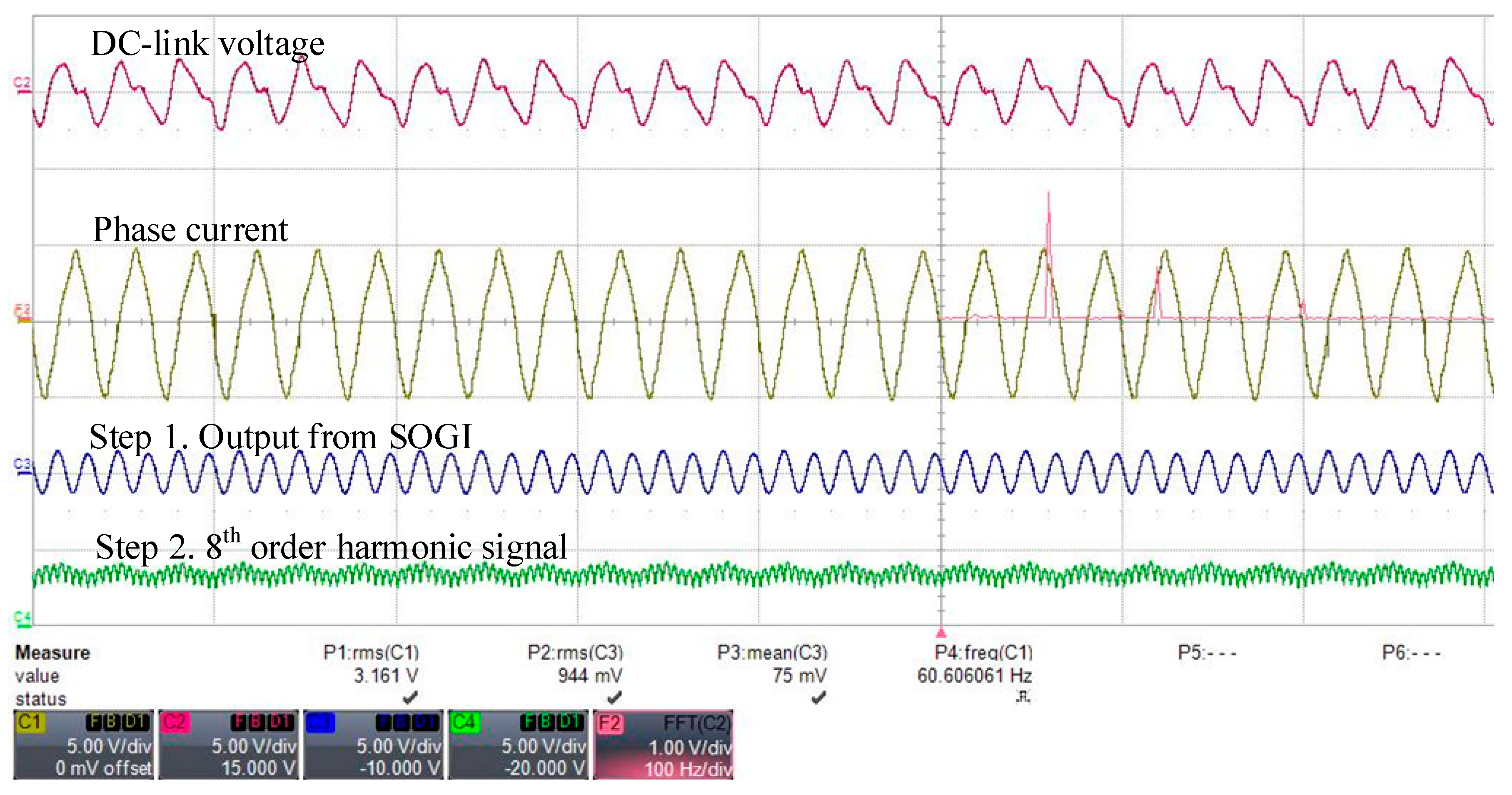
The proposed DC offset error compensation algorithm was implemented in the experiment. Figure 10 shows experimental results at steady state.
The experimental results in Figure 10 show DC-link voltage, phase current and the output signal from SOGI and the eighth order harmonic signal. The output signal from SOGI and the eighth order harmonic signal correspond to the signals at Step 1 and Step 2 as introduced in Figure 3.
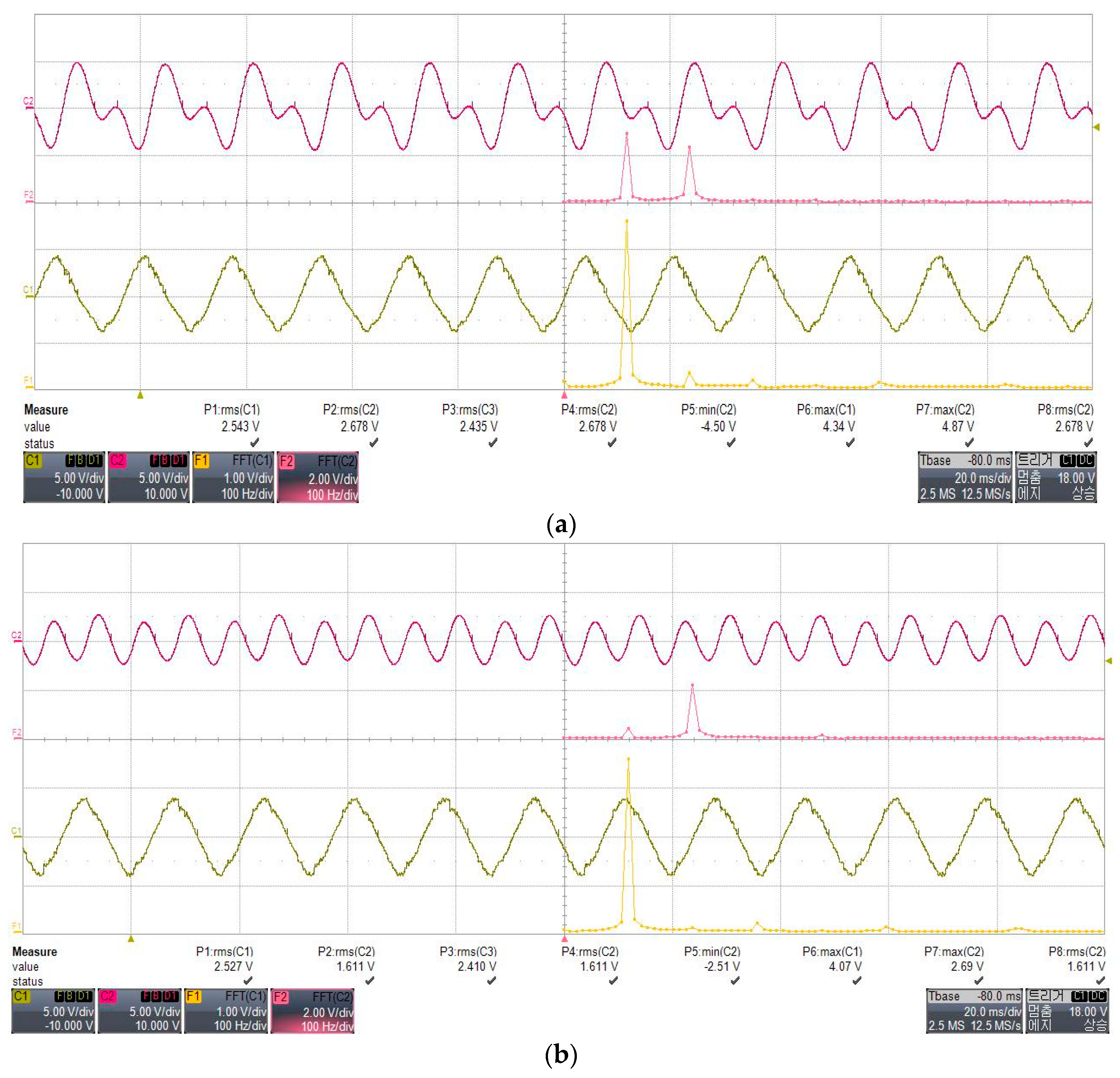
In Figure 11, experimental results of phase current and DC-link voltage with and without applying the DC offset error compensation algorithm are shown. Experimental results of a frequency spectrum and experimental data at a time domain are overlaid in Figure 11. During the experiment, 0.3 A of DC offset current was injected when the DC-link voltage was 330 V. Figure 11a shows the experimental results when the proposed method is not applied. As seen in the results, harmonic components are easily detected in DC-link voltage and phase current is non-sinusoidal due to harmonics in a time domain. From frequency spectrum analysis results of the uncompensated signal, harmonics in DC-link voltage and phase current are clearly represented in Figure 11. Especially for phase current, the DC component and second harmonic component are detected as theoretically analyzed in Equation (8). In a vertical axis of Figure 11, DC link voltage is 2.5 V per division and current is 1.5 A per division. Figure 11b shows the experimental results when the proposed method is applied. As shown in the time domain experimental results, a significant reduction of harmonic components in DC-link voltage and phase current are observed. From frequency spectrum analysis results of the compensated signal, it is shown that harmonics in DC-link voltage and phase current are eliminated. In addition, THD of the current was calculated from the experimental results. The calculated THD of phase current was reduced from 15.8% to 5.8% when the proposed algorithm was applied. The effect of dead time, undesired noise from sensor, and an interface circuit seem to be reasons for the THD difference between simulation and experimental results. From the experimental results, it is verified that specific harmonic signals generated by the DC offset error are eliminated by applying the proposed DC offset error compensation method and quality of phase current is improved.
In Figure 12, the experimental results of robustness evaluation of the proposed algorithm are shown. While 0.3 A of DC offset error was applied on purpose, the proposed DC offset compensation algorithm was applied at 1.8 s. Then, it took approximately 2 s until the applied DC offset was compensated and we investigated whether the ripple on the DC-link voltage was reduced. At 7.3 s, the proposed DC offset compensation algorithm was ended. As soon as the compensation algorithm was disabled, ripple on the DC-link voltage and offset on the phase current were observed. When the DC offset error compensation algorithm was enabled and disabled, the effect on the phase current such as fluctuation was barely seen as shown in Figure 12.
In addition to the robustness evaluation, dynamic performance of the proposed algorithm was evaluated experimentally. The experimental results are shown in Figure 13.
In Figure 13, 0.3 A of DC offset current was applied initially and the proposed DC offset compensation algorithm was applied. From the experimental results, it can be observed that harmonics signals on DC-link voltage are significantly reduced and offset in phase current is adjusted. In addition, the settling time of extracted DC offset component and the compensation signal can be investigated. The extracted DC offset component and the compensation signals correspond to the output signals of Step 3 and Step 4 in Figure 3. As shown in Figure 13, the settling time of the compensation signal is approximately 4 s. Transient dynamic performance can be adjusted if it is needed by tuning controller gain. During the controller gain design process, the tradeoff between dynamic performance and filtering performance of a controller should be considered.
6. Conclusions
In this paper, causes of DC offset error in the phase current measuring process and effects of DC offset error in phase current on a grid side are theoretically analyzed. From the analysis, we investigated whether current DC offset error generates an additional DC component and second harmonic component. Using the analysis result, the DC offset error compensation algorithm for variable and unpredictable DC offset signal is proposed for a single-phase grid-tied inverter system and the DC offset error is estimated and directly eliminated. The proposed DC offset error compensation algorithm is verified in simulation and experiment in this paper. Applying the proposed DC offset error compensation algorithm, it is verified that quality of phase current and DC-link voltage is significantly improved.
Author Contributions
J.S.L. took a role in investigation and writing a paper. S.-H.H. proposed the DC offset compensation algorithm and directs the research.
Funding
This research was supported by the Korea Electric Power Corporation through Korea Electrical Engineering & Science Research Institute [Grant number: R17XA05-7] and the National Research Foundation of Korea (NRF-2017R1D1A1B03 031807).
Acknowledgments
This research was supported by the Korea Electric Power Corporation through Korea Electrical Engineering & Science Research Institute [Grant number: R17XA05-7] and the National Research Foundation of Korea (NRF-2017R1D1A1B03 031807).
Conflicts of Interest
The authors declare no conflict of interest.
References
- Carrasco, J.M.; Franquelo, L.G.; Bialasiewicz, J.T.; Galvan, E.; Guisado, R.C.P.; Prats, M.A.M.; Leon, J.I.; Moreno-Alfonso, N. Power electronic systems for the grid integration of renewable energy sources: A survey. IEEE Trans. Ind. Electron. 2006, 53, 1002–1016. [Google Scholar] [CrossRef]
- Gu, B.; Dominic, J.; Lai, J.; Chen, C.; LaBella, T.; Chen, B. High reliability and efficiency single phase transformerless inverter for grid-connected photovoltaic system. IEEE Trans. Power Electron. 2013, 28, 2235–2245. [Google Scholar] [CrossRef]
- Lee, C.H.; Choi, J.W. Compensation strategy to eliminate the effect of current measurement offsets in grid-connected inverters. J. Power Electron. 2014, 14, 383–391. [Google Scholar] [CrossRef]
- Berba, F.; Atkinson, D.; Armstrong, D. A review of minimisation of output DC current component methods in single phase grid connected inverters PV applications. In Proceedings of the 2012 2nd International Symposium on Environment Friendly Energies and Applications, Newcastle Upon Tyne, UK, 25–27 June 2012. [Google Scholar]
- Blewitt, W.; Atkinson, D.; Kelly, J.; Larkin, R. Approach to low cost prevention of DC injection in transformerless grid connected inverters. IET Power Electron. 2010, 3, 111–119. [Google Scholar] [CrossRef]
- Buticchi, G.; Lorenzani, E.; Franceschini, G. A DC offset current compensation strategy in transformerless grid-connected power converters. IEEE Trans. Power Deliv. 2011, 26, 2743–2751. [Google Scholar] [CrossRef]
- Bowtell, L.; Ahfock, A. Direct current offset controller for transformerless single-phase photovoltaic grid-connected inverters. IET Renew. Power Gener. 2010, 4, 428–437. [Google Scholar] [CrossRef] [Green Version]
- Bowtell, L.; Ahfock, A. Dynamic analysis of a DC offset controller for grid-connected inverters. In Proceedings of the 2010 20th Australasian Universities Power Engineering Conference, Christchurch, New Zealand, 5–8 December 2010. [Google Scholar]
- Menniti, D.; Pinnarelli, A. A novel compensation approach for DC current component in a grid-connected photovoltaic generation system. In Proceedings of the 2012 IEEE Power and Energy Society General Meeting, San Diego, CA, USA, 22–26 July 2012. [Google Scholar]
- Song, W.; Feng, X.; Smedley, K.M. A carrier-based PWM strategy with the offset voltage injection for single-phase three-level neutral-point-clamped converters. IEEE Trans. Power Electron. 2013, 28, 1083–1095. [Google Scholar] [CrossRef]
- Park, G.; Hwang, S.; Kim, J.; Lee, K.; Lee, D. Reduction of current ripples due to current measurement errors in a doubly fed induction generator. J. Power Electron. 2010, 10, 313–319. [Google Scholar] [CrossRef]
- Xu, S.; Wang, J.; Xu, J. A current decoupling parallel control strategy of single phase inverter with voltage and current dual closed loop feedback. In Proceedings of the 2010 IEEE Energy Conversion Congress and Exposition, Atlanta, GA, USA, 12–16 September 2010. [Google Scholar]
- Fischer, R.J.; González, S.A.; Carugati, I.; Herrán, M.A.; Judewicz, M.G.; Carrica, D.O. Robust predictive control of grid-tied converters based on direct power control. IEEE Trans. Power Electron. 2013, 29, 5634–5643. [Google Scholar] [CrossRef]
- Chen, D.; Zhang, J.; Zhang, Z. An improved repetitive control scheme for grid-connected inverter with frequency-adaptive capability. IEEE Trans. Ind. Electron. 2013, 60, 814–823. [Google Scholar] [CrossRef]
- Karimi-Ghartemani, M.; Khajehoddin, S.A.; Jain, P.; Bakhshai, A. Linear quadratic output tracking and disturbance rejection. Int. J. Control 2011, 84, 1442–1449. [Google Scholar] [CrossRef]
- Khajehoddin, S.A.; Karimi-Ghartemani, M.; Bakhshai, A.; Jain, P. High quality output current control for single phase grid-connected inverters. In Proceedings of the 2014 IEEE Applied Power Electronics Conference and Exposition—APEC 2014, Fort Worth, TX, USA, 16–20 March 2014. [Google Scholar]
- Castilla, M.; Miret, J.; Matas, J.; De Vicuna, L.G.; Guerrero, J.M. Control design guidelines for single-phase grid-connected photovoltaic inverters with damped resonant harmonic compensators. IEEE Trans. Ind. Electron. 2009, 56, 4492–4501. [Google Scholar] [CrossRef]
- Silwal, S.; Karimi-Ghartemani, M. On the design of proportional resonant controllers for single-phase grid-connected inverters. In Proceedings of the 2016 12th IEEE International Conference on Control and Automation (ICCA), Kathmandu, Nepal, 1–3 June 2016. [Google Scholar]
- Kim, D.; Kim, J.; Park, J.; Hwang, S. Compensation of current measurement error in half bridge PWM inverter for linear compressor. In Proceedings of the 2013 IEEE ECCE Asia Downunder, Melbourne, VIC, Australia, 3–6 June 2013. [Google Scholar]
Figure 1.
A proportional-resonant (PR) current control-based system block diagram of a single-phase grid-tied inverter.
Figure 1.
A proportional-resonant (PR) current control-based system block diagram of a single-phase grid-tied inverter.

Figure 2.
Current measurement process in a single-phase grid-tied system and direct current (DC) offset error occurrence in a current measuring process.
Figure 2.
Current measurement process in a single-phase grid-tied system and direct current (DC) offset error occurrence in a current measuring process.

Figure 3.
A block diagram of a single-phase grid-tied control system containing the proposed DC offset error compensation algorithm.
Figure 3.
A block diagram of a single-phase grid-tied control system containing the proposed DC offset error compensation algorithm.

Figure 4.
Transformation of signals during signal processing in the proposed DC offset compensation algorithm. (a) Fundamental and the second harmonic signal extracted by the SOGI; (b) Absolute signals of second harmonic signal and its 90 degree shifted signal. Eighth order signal generated by adding second harmonic signal and its 90 degree shifted signal.

Figure 5.
An entire system block diagram of the proposed DC offset error compensation algorithm developed for MATLAB/Simulink simulation.
Figure 5.
An entire system block diagram of the proposed DC offset error compensation algorithm developed for MATLAB/Simulink simulation.

Figure 6.
Simulation results of (a) phase current (b) DC-link voltage without DC offset compensation algorithm and (c) phase current and (d) DC-link voltage applying the proposed DC offset error compensation algorithm.
Figure 6.
Simulation results of (a) phase current (b) DC-link voltage without DC offset compensation algorithm and (c) phase current and (d) DC-link voltage applying the proposed DC offset error compensation algorithm.

Figure 7.
Frequency spectrum of phase current: (a) without applying a compensation algorithm; (b) with applying the proposed compensation algorithm.
Figure 7.
Frequency spectrum of phase current: (a) without applying a compensation algorithm; (b) with applying the proposed compensation algorithm.

Figure 8.
A block diagram of the experimental set-up for a single-phase grid-tied inverter system.

Figure 9.
A picture of the experimental set-up for a single-phase grid-tied inverter system.

Figure 10.
Steady state experimental results of a single-phase grid-tied inverter system.

Figure 11.
Experimental results of DC-link voltage and phase current of (a) without and (b) with applying the proposed DC offset error compensation algorithm.
Figure 11.
Experimental results of DC-link voltage and phase current of (a) without and (b) with applying the proposed DC offset error compensation algorithm.

Figure 12.
Experimental results of DC-link voltage and grid phase current when the proposed compensation is started and ended.
Figure 12.
Experimental results of DC-link voltage and grid phase current when the proposed compensation is started and ended.

Figure 13.
Experimental results of the dynamic characteristic of the proposed DC compensation algorithm.
Figure 13.
Experimental results of the dynamic characteristic of the proposed DC compensation algorithm.


Table 1.
Single-Phase Grid-tied Inverter Specifications.
| Parameters | Value | |
|---|---|---|
| Rated power | 3 (kW) | |
| Grid voltage | 220 (V), 60 (Hz) | |
| DC link capacitance | 5240 (μF) | |
| Filter inductance | 5 (mH) | |
| Filter capacitance | 10 (μF) | |
| Sampling period | 100 (μs) | |
| Switching frequency | 10 (kHz) | |
| Current sensor (LA55-P) | Offset current @ IP = 0, TA = 25 °C | ±0.1 (mA max) |
| Temperature variation @ TA = −25 °C ~ +85 °C | ±0.3 (mA max) | |
| Accuracy @ IPN, TA = 25 °C | ±0.65 (%) | |
| Op-amp(TL084C) | Input offset voltage | 20 (mV max) |
| Temperature coefficient of input offset voltage | 18 (μV/°C) | |
| ADC(AD7864-1) | Resolution | 12-bit |
| Bipolar zero error(=offset error) | ±3 (LSB max) | |
© 2018 by the authors. Licensee MDPI, Basel, Switzerland. This article is an open access article distributed under the terms and conditions of the Creative Commons Attribution (CC BY) license (http://creativecommons.org/licenses/by/4.0/).
Share and Cite
MDPI and ACS Style
Lee, J.S.; Hwang, S.-H. DC Offset Error Compensation Algorithm for PR Current Control of a Single-Phase Grid-Tied Inverter. Energies 2018, 11, 2308. https://doi.org/10.3390/en11092308
AMA Style
Lee JS, Hwang S-H. DC Offset Error Compensation Algorithm for PR Current Control of a Single-Phase Grid-Tied Inverter. Energies. 2018; 11(9):2308. https://doi.org/10.3390/en11092308
Chicago/Turabian StyleLee, Jae Suk, and Seon-Hwan Hwang. 2018. "DC Offset Error Compensation Algorithm for PR Current Control of a Single-Phase Grid-Tied Inverter" Energies 11, no. 9: 2308. https://doi.org/10.3390/en11092308
Note that from the first issue of 2016, this journal uses article numbers instead of page numbers. See further details here.