Hybrid Model Predictive Control Strategy of Supercapacitor Energy Storage System Based on Double Active Bridge

1
Hubei Key Laboratory for High-Efficiency Utilization of Solar Energy and Operation Control of Energy Storage System, Hubei University of Technology, Wuhan 430068, China
2
College of Electrical Engineering, Zhejiang University, Hangzhou 310027, China
*
Author to whom correspondence should be addressed.
Energies 2019, 12(11), 2134; https://doi.org/10.3390/en12112134
Submission received: 19 April 2019
/
Revised: 23 May 2019
/
Accepted: 30 May 2019
/
Published: 4 June 2019
(This article belongs to the Special Issue Advances in Supercapacitor Technology and Applications)
Abstract
:In order to solve the problem of which the dynamic response of a supercapacitor (SC) is limited due to the mismatch dynamic characteristics between the DC/DC converter and supercapacitor in an energy storage system, this paper proposes a hybrid model predictive control strategy based on a dual active bridge (DAB). The hybrid model predictive control model considers the supercapacitor and DAB in a unified way, including the equivalent series resistance and capacitance parameters of the SC. The method can obtain a large charging and discharging current of the SC, thereby not only improving the overall response speed of the system, but also expanding the actual capacity utilization range of the SC. The simulation results show that compared with the model prediction method of the dual active bridge converter, the proposed control method can effectively improve the overall response speed of the system, which can be improved by at least 0.4 ms. In addition, the proposed method increases the actual upper limit of the SC voltage, reduces the actual lower limit of the SC voltage, and then expands the actual capacity utilization range of the SC by 18.63%. The proposed method has good application prospects in improving the dynamic response performance of energy storage systems.
1. Introduction
Supercapacitors (SCs) have developed rapidly in recent years due to their large capacity, high power density [1], high charge-discharge rate, high conversion efficiency, wide operating temperature range, no pollution, and convenient control. However, due to the wide range of terminal voltages during the storage and release of energy in an SC, the systems used in actual energy storage systems are usually equipped with bidirectional DC/DC converters to implement power conversion [2].
In addition, since an SC voltage unit is low [3], many units should be connected in series in actual use, causing the problem of equalization. For some applications, where the DC bus voltage is relatively large, such as a three-phase grid-connected inverter, a high-gain bidirectional DC converter suitable for a wide voltage range is needed to adjust the output voltage to meet the energy requirements of the DC bus [4]. In recent years, dual active bridge bidirectional DC-DC converters are commonly used in medium power applications [5], which enable a soft switching operation over a wide voltage range. Additionally, the transformer turns ratio can be used to obtain a high gain output [6]. In addition, the DAB converter has the advantages of a high power-density, bidirectional transmission power, high efficiency, and structural symmetry [7,8]. Due to the large number of switches in a DAB converter, the control process is generally complicated, so the response time of the converter is longer than with an SC [9], which does not reflect the fast response characteristics of SCs. In order to improve the dynamic response speed of the converter when the load is abrupt or the input voltage fluctuates, some scholars have proposed related control methods.
In [10], an inductor current boundary control method was proposed based on tradition inductor current peak control and single-phase shift control. The boundary control method significantly speeds up the dynamic response of the DC-DC converter when the load suddenly changes, but the method is too complicated and requires up to five Hall sensors. In [11], a load current feedforward control method was proposed based on direct power control, which introduces the load current into the control system, significantly improving the load response speed of the converter. However, it did not analyze the response characteristics of the converter when the input voltage was changed. In [12], based on the idea of direct power control, a virtual direct power control strategy was proposed, which introduces input voltage and load current information at the same time, so that the converter achieves a fast dynamic response. In [13], based on the working principle of a dual-active bridge DC-DC converter, the principle of single-phase shift control, and the steady-state characteristics of the output current, an output current control method based on the input voltage feedforward was proposed to improve the dynamic characteristics of the converter. This method is based on the research of the dual active bridge DC-DC converter as the current source. In [14], a model predictive control strategy was proposed based on the establishment of the state space average model of a DAB by analyzing the characteristics of a DAB and using the traditional phase shift control as an example. The proposed method significantly improved the dynamic characteristics of the converter for the input voltage’s abrupt change and the load’s abrupt change compared with the traditional voltage closed-loop control method.
In order to improve the overall response speed of a super-capacitor energy storage system based on dual active bridges, a hybrid model predictive control strategy with a fast dynamic response time is proposed. First, the overall structure model of the energy storage system based on a combined appropriate SC equivalent model and a DAB converter model is established in this paper. Then, the working principle of a DAB based on traditional phase shift control is analyzed, and the state space average model of the energy storage system composed of a DAB converter and SC is established. By selecting the appropriate evaluation target and establishing the cost function, a model predictive control strategy incorporating the parameters of the SC equivalent model is proposed to manage the energy of the system. Finally, the effectiveness of the proposed control strategy is verified by simulations in Matlab (9.2.0.538062 (R2017a), MathWorks, Natick, Massachusetts, America) software and experiments.
2. Working Principle of the DAB-SC System
2.1. SC Model
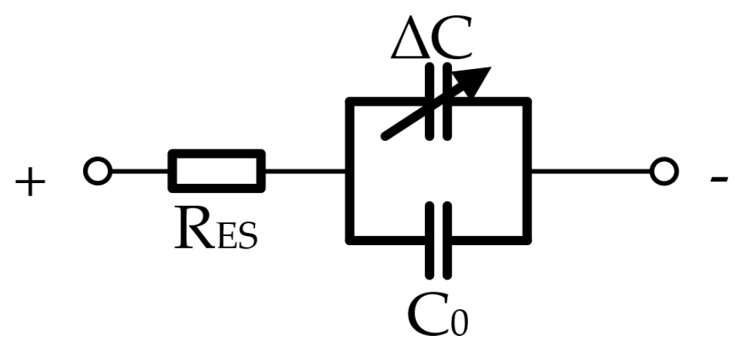
The structure of the SC unit is mainly composed of electrodes, electrolytes, diaphragms, and packaging, and each component has an important impact on its performance. Thus, it is necessary to build a precise and applicable SC model in circuit analysis. Scholars have proposed many SC equivalent models based on the physical structure and charging and discharging conditions, such as the first-order classical resistor-capacitor (RC) model, RC transmission line model, multi-branch RC parallel model, frequency domain model [15], and artificial neural network (ANN) model. By combining various SC models to obtain a general model, the general SC equivalent circuit model can be simplified based on characteristics, such as: Large-scale modularization of SCs, high charging and discharging power, and high charging and discharging frequency. The simplified model is shown in Figure 1.
The use of SCs for large-scale energy storage requires identification of the SC parameters. In the simplified equivalent circuit model of the SC unit, RES is the equivalent series resistance, which not only characterizes the heat loss inside an SC, but also causes different voltage drops as the discharge current changes. Thus, RES affects the maximum value of the discharge current to a certain extent. The magnitude of RES generally does not change with external factors [16], and is usually measured by a classical model.
When the charge and discharge conditions of the SC are determined, the main factor that affects the value of the variable capacitor in the equivalent circuit is the actual operating voltage [17]. In order to identify the parameters of the SC unit, several sets of tests are needed, by charging the SC unit to different voltage levels with a constant frequency.
According to Equation (1), the actual capacitance of an SC unit in different sets of tests can be calculated:
In Equation (1), QSC is the amount of charge of an SC; ΔUSC is the actual voltage change; ISC is the SC current; ΔT is the charging and discharging time; ΔUC is the total voltage change; ΔUESR is the voltage drop caused by ESR.
After processing the (Ucharge, Cactual) data-points by the linear fitting method, the relationship between the capacitance and voltage of a SC can be obtained as shown in Equation (2):
In Equation (2), Cactual is the actual capacitance of an SC at different voltages; ΔC is the variable capacitance; C0 is the initial capacitance of an SC; Kv is the coefficient of variation of the SC capacitance with the voltage; Ucharge is the SC’s actual voltage.
In this paper, through the linear fitting of graphic data in [18], the voltage and capacitance data of Maxwell’s 1 F SC were obtained, and then the data of the 125 V, 63 F SC, which was used in this paper, was obtained according to the string and parallel relationship of the capacitor. The 125 V, 63 F SC is made up of 46 modules in series, and the module was obtained by paralleling 2900 Maxwell’s 1 F, 2.7 V SC units. Additionally, the obtained data of the 125 V, 63 F SC were linearly fitted to obtain a relation as shown in Equation (3):
2.2. Principle Analysis of DAB
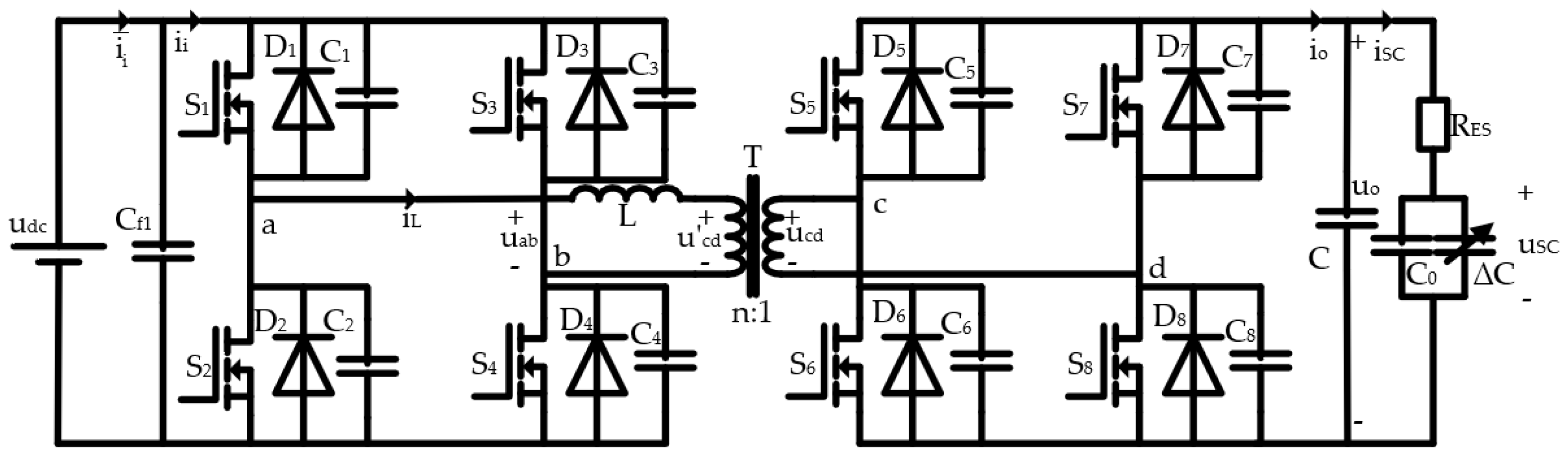
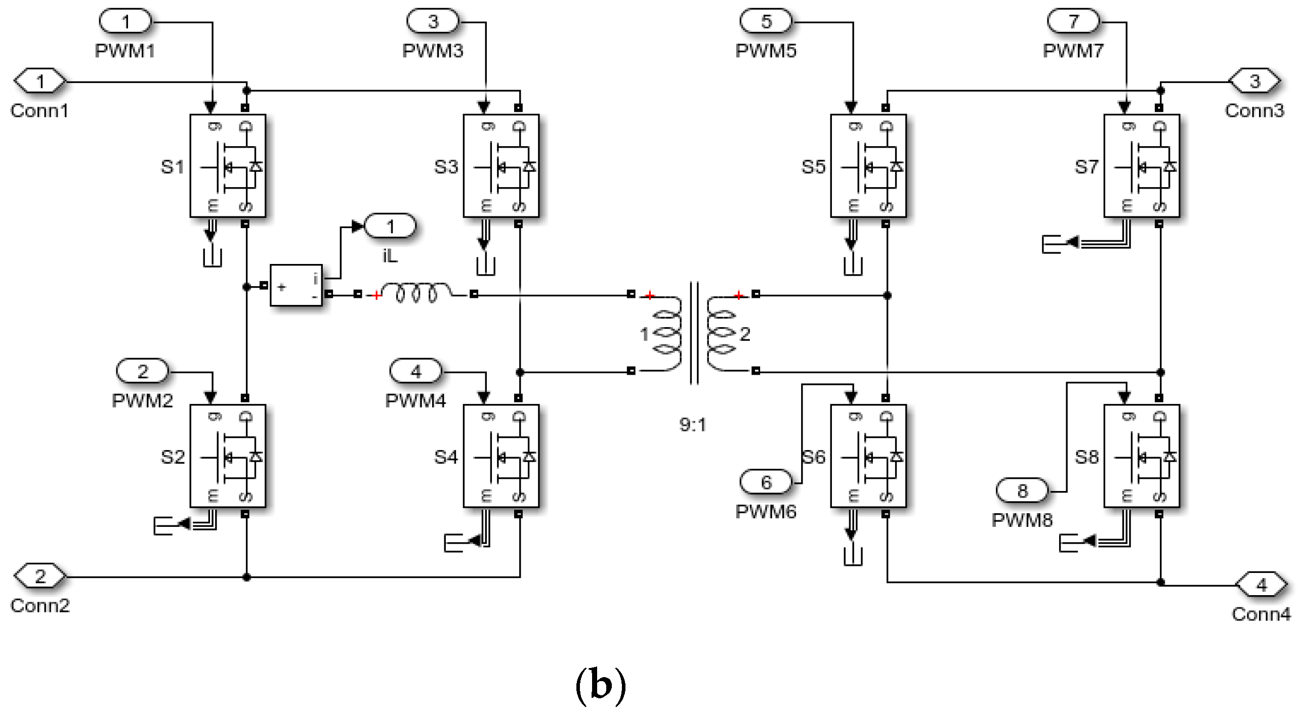
The DAB converter acts as an interface between the SC and DC bus. Generally, there are two basic control methods for the DAB converter: The first is pulse width modulation control; the second is phase shift control. Phase shift control is simpler and easier to implement than the first. Therefore, most DAB controls adopt the phase shift control method [19]. Taking single-phase shift as an example, when a single DAB is in normal operation, the switching frequencies of the H-bridges on both sides of the isolation transformer are the same, and the two H-bridges output square-wave voltages, uab and ucd, respectively, with a duty ratio of 50%. When the phase of the uab leads the ucd, the energy is forwardly transmitted; that is, from udc to uo. Otherwise, the energy is reversely transmitted. Therefore, by controlling the degree of the phase shift angle between the two square wave voltages, the transferred energy can be controlled.
Figure 2 shows the topology of the DAB-SC system. Figure 3 shows the main working waveform of the converter with the phase shift control method. The two switches on each bridge arm are complementarily turned on, and the diagonal switches are turned on or off at the same time. The power is controlled by controlling the phase shift angle between the midpoint voltages, uab and ucd, of the primary and secondary side arms. Ts is half of the switching frequency, Ts = 1/(2fs), and D represents the phase shift between uab and ucd, where D = ton/Ts, and −1 < D < 1. The working principles of the converter when transmitting power in the forward and reverse directions are similar. This paper utilized the forward direction as an example to analyze the operating characteristics of the DAB converter. Before the analysis, the following assumptions were made: (1) The converter is in steady state operation; (2) all switches are regarded as ideal switches with a reverse parallel diode, and the parasitic capacitance is connected in parallel; (3) the size of L is equal to the sum of the leakage inductance of the transformer and the applied inductance; (4) the transformer is ideal, the excitation current is zero; and (5) udc > nuo, where n is the turns ratio of the transformer.
When the converter is working in the forward direction, the driving signals of S1, S4 and S2, S3 are ahead of S5, S8 and S6, S7 respectively, as shown in Figure 3a. In the figure, u’cd is the voltage of ucd converted to the primary side; uL is the voltage across the inductor, L; and iL is the inductor current.
Under steady-state conditions, the relationship between the transmission power of the DAB and the amount of phase shift is as shown in Equation (4):
It can be known from Equation (4) that the transmission power reaches maximum when D = 0.5 in the forward transmission, and when D = −0.5 in the reverse transmission. Typically, the DAB converter operates in the range of D∈[−0.5, 0.5].
The output power of the DAB can also be expressed as Po = uoio, and the relationship between the output current of the DAB converter and the phase shift amount can be obtained as shown in Equation (5):
In the DAB converter, there are two key parameters, which are the transformer ratio, n, and the buffer inductance, L. When the input voltage of the DAB converter is equal to the value of the output voltage converted to the primary side, the current stress of the device is minimized. By considering the actual fluctuation of the input and output voltages, the transformer ratio can be selected to make the rated input voltage equal to the value of the rated output voltage converted to the primary side. For example, when the rated voltages of the input and output voltages are 700 V and 75 V, respectively, the transformer ratio is determined to be n = 700/75 ≈ 9.
The zero voltage switch (ZVS) range of the device and the suppression of the reactive power are mutually contradictory. A larger ZVS range of a device requires larger inductor values; however, for the suppression of the reactive power, the smaller the inductor value, the better [20], which is a contradiction. The focus of this paper was to study the response speed of the system, and thus the influence of ZVS was not considered. Therefore, a small inductance value as selected for the research.
2.3. State Space Average Model of DAB-SC
In order to establish the state space average model of the DAB, the output capacitor voltage and the inductor current were selected for modeling. It can be seen from Figure 3a that when the voltage, uab, leads the voltage, ucd, the energy is transmitted forward, 0 < D < 0.5. The overall DAB-SC system has six working states in one switching cycle, and a system of differential equations can be established in each working state. According to Kirchhoff’s law, the differential equations, Equations (6)–(11), can be obtained:
For each differential equation, it can only represent the voltage–current relationship in this operating state. Therefore, it is necessary to establish a differential equation that can describe the characteristics of the converter over the entire switching period. It is worth noting that in the DAB, the inductor current is a pure alternative current (AC) component whose average value is zero during one switching cycle, so the average value of the inductor current is meaningless. Therefore, a simplified reduction model of the DAB module can be obtained by eliminating the inductor current as shown in Equation (12):
Similarly, when the voltage, ucd, leads uab, the energy is reversely transmitted; that is, −0.5 < D < 0, and the simplified reduced-order model of the DAB module is shown in Equation (13):
In conclusion, when −0.5 < D < 0.5, the simplified reduced-order model of the DAB module is as shown in Equation (14):
3. Management Strategy
The state of charge (SOC) reflects the remaining capacity of the SC. In a photovoltaic system equipped with energy storage, by accurately estimating the SOC, how long the SC can work under a current load can be determined. There is a definite relationship between the energy, ESC, stored by the SC and the terminal voltage, as shown in Equation (15):
Therefore, it is only necessary to detect the SC voltage to accurately determine its SOC. The relationship between the voltage of the SC and the SOC is as shown in Equation (16):
In Equation (16), CSC is the capacity of the SC, Uo is the SC’s terminal voltage, and UN is the rated voltage of the SC.
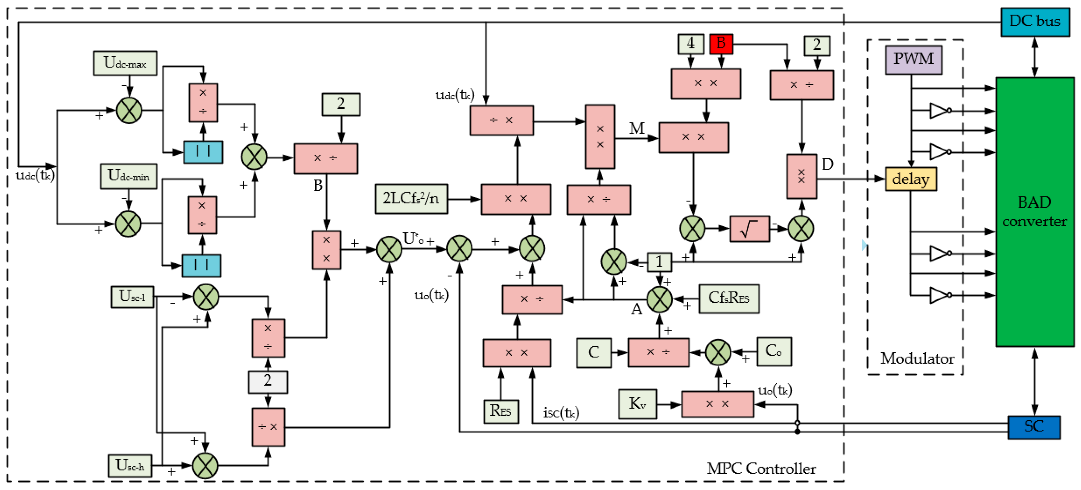
Based on the relationship between the terminal voltage and the SOC, the system can be managed by controlling the terminal voltage. Six voltage limits were set: The DC bus voltage upper limit, Udc_max; lower limit, Udc_min; SC upper limit voltage, Usc_max; lower limit voltage, Usc_min; upper limit warning voltage, Usc_h; and lower limit warning voltage, Usc_l. The working principle is as follows: When the DC bus voltage exceeds Udc_max and the SC voltage is close to Usc_min, the SC can be charged with a large current. As the SC voltage increases, the phase shift duty ratio of the DAB converter is changed by predictive control in order to prevent overcharging and to increase the upper limit of the actual SC charging voltage; when the DC bus voltage exceeds Udc_min, and the SC voltage is close to Usc_max, the SC performs a large current discharge. As the SC voltage decreases, the phase shift duty ratio of the DAB converter is also changed by predictive control in order to prevent over discharging and to decrease the lower limit of the actual SC charging voltage.
According to the State Grid Corporation “DC Power System Technical Supervision Regulations” and other relevant standards and specifications, when the DC bus power supply is continuously supplied, normal fluctuation of the grid voltage should be no more than 10% of the rated voltage [21]. The rated DC bus voltage of the microgrid in this paper was set at 700 V with a fluctuation of ±5%; that is, Udc_min = 665 V, and Udc_max = 735 V. The SC had a rated voltage of 125 V and the upper limit warning voltage and the lower limit warning voltage were 40%–80%.
In summary, the coordinated control strategy of the energy storage systems is as follows: a) In the shutdown state of an energy storage system, the DAB converter is in an idle state and is not charged or discharged; b) in the SC charging area, when the DC bus voltage, Udc, satisfied that Udc > 735 V, and SOCsc ≤ 80%, the SC is charged to absorb excess power in the DC bus; and c) in the SC discharge area, when the DC bus voltage satisfied that Udc < 665 V, and SOCsc > 40%, the SC discharges, supplementing the power shortage in the DC bus.
4. Model Predictive Control
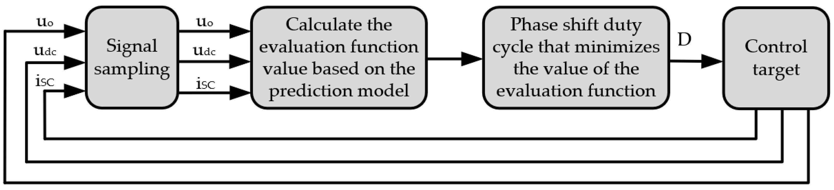
Model predictive control (MPC) is an active control strategy based on the mathematical model of the converter and is adjusted by predicting the change trend of the control variables. It predicts the optimality of the next moment based on the circuit parameters and the sampling information at the current time to minimize the deviation between the output and the reference. There are many forms of the MPC algorithm, and all MPC algorithms have three basic characteristics: Prediction model, rolling optimization, and feedback correction. A schematic diagram of the MPC strategy of the DAB-SC system studied in this paper is shown in Figure 4, where uo is the DAB output voltage, udc is the DC bus voltage, and iSC is the SC current.
4.1. Establishment of the Prediction Model for the DAB-SC System
The derivative of the output voltage in Equation (14) reflects the trend of the output voltage. Additionally, the Euler forward method can be used to discretize Equation (14), and then Equation (17) can be obtained:
Equation (17) can be simplified with Equation (14) to obtain Equation (18):
The SC has a high-power density characteristic and can provide a large instantaneous current, thus the current flowing through SC at time tk+1 was set to be iSC(tk+1). Then, Equation (19) can be established:
By substituting Equation (19) into Equation (18), Equation (20) can be obtained:
In Equation (20), uo(tk) and udc(tk) represent the DAB output voltage and DC bus voltage, respectively, sampled at time tk; uo(tk+1) represents the predicted value of the SC voltage at time tk+1.
According to the general characteristics of the capacitor, the equation of the equivalent capacitor in the SC equivalent model can be obtained, as shown in Equation (21):
where dt = 2Ts in Equation (21). In order to reflect the fast response characteristic of the SC, we chose iSC in Equation (21) to be iSC(tk+1). Then, Equation (22) can be obtained:
According to Equation (2), the relationship between the capacitance of the SC and the actual voltage across the SC is as shown in Equation (23):
According to Equation (22) and Equation (23), taking the average value of each state in the case of the charging and discharging of the SC, Equation (24) can be obtained:
By joining Equation (20) and Equation (24) together to eliminate iSC(tk), Equation (25) can be obtained:
where the value of A is as shown in Equation (26):
4.2. Phase Shift Optimization Calculation and Analysis
For energy storage systems with a DAB, the primary control objective is to stabilize the DC bus voltage. When the bus voltage is too high, the SC needs to be charged. When the bus voltage is low, the SC is required to discharge.
Therefore, different SC reference voltages were selected in this paper. When the bus voltage is high, the SC reference value takes the upper limit warning voltage, Usc_h; when the bus voltage is low, the SC reference value takes the lower limit warning voltage, Usc_l. The value of the SC reference value is shown in Equation (27):
The deformation of Equation (27) is given by Equation (28):
The value of B in Equation (28) is as shown in Equation (29):
Therefore, a cost function is established based on the prediction model of Equation (26) of the output voltage as shown in Equation (30):
In order to minimize the deviation between the output voltage and the reference voltage in the next moment, the cost function needs to be minimized; that is, the selected optimal phase shift amount should minimize the cost function value. By combining Equations (25), (28), and (29) and deriving Equation (30), the value of D can be obtained as in Equation (31):
The value of M in Equation (31) is as shown in Equation (32):
A block diagram of the MPC structure constructed according to Equation (32) is shown in Figure 5.
It can be seen from the above analysis that the optimal phase shift of the DAB converter in the proposed method is obtained based on the sampling voltage, sampling current, and circuit parameters of the DAB-SC system. Additionally, the parameters of the SC can reflect the fast response characteristics of the SC. Compared with predictive control based on the simple construction of a DAB converter, the proposed control strategy makes the overall response of the DAB-SC system faster.
5. Simulation Analysis
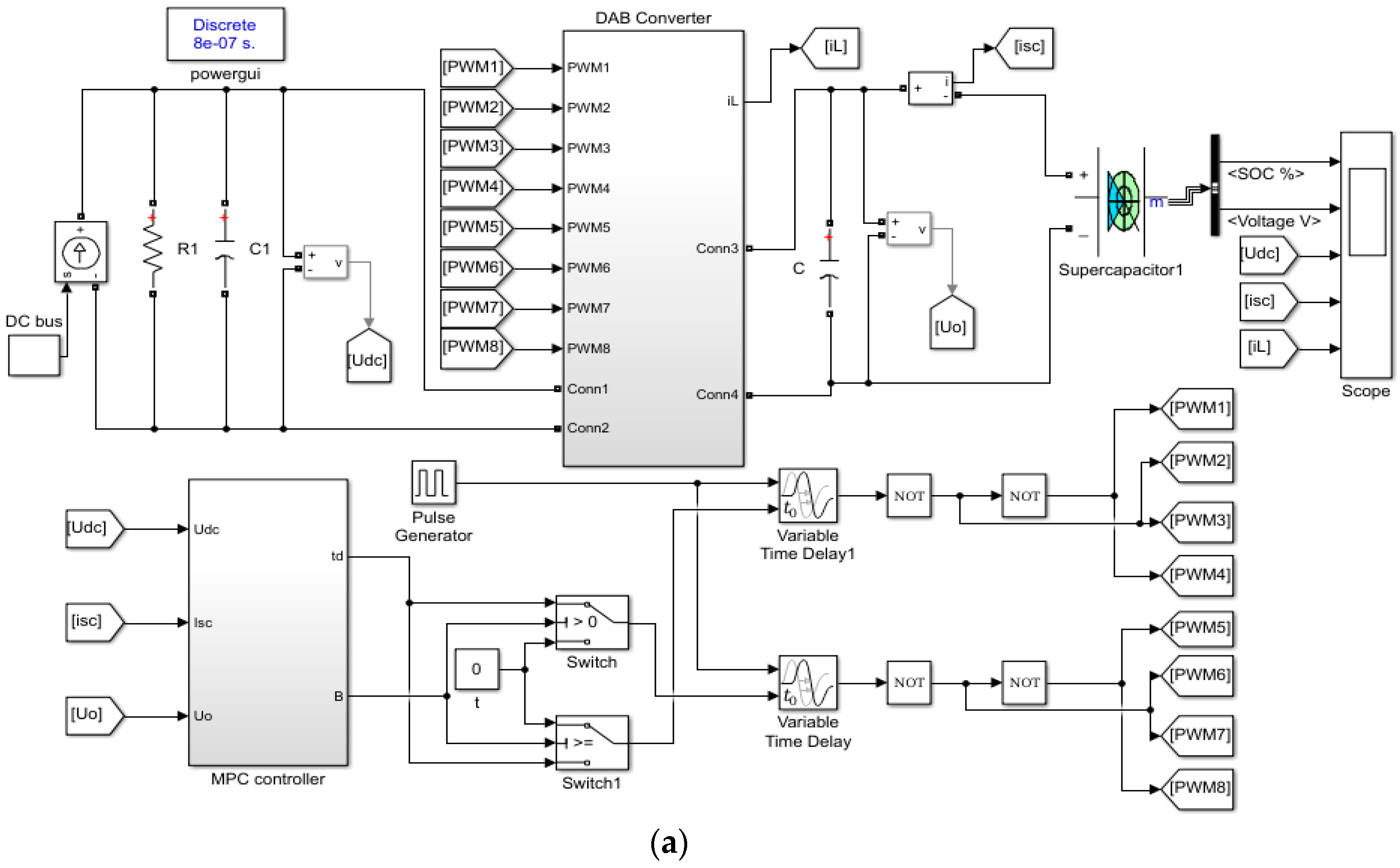
A simulation model of the DAB-SC system, as shown in Figure 6, was built in MATLAB/simulink according to the topology diagram of Figure 2 and the control block diagram of Figure 5. The parameters of the simulation are shown in Table 1. Additionally, the experimental simulation pulse signal generator had a frequency of 20 kHz and a duty cycle of 50%.
5.1. SC Discharge in the Normal Working Range
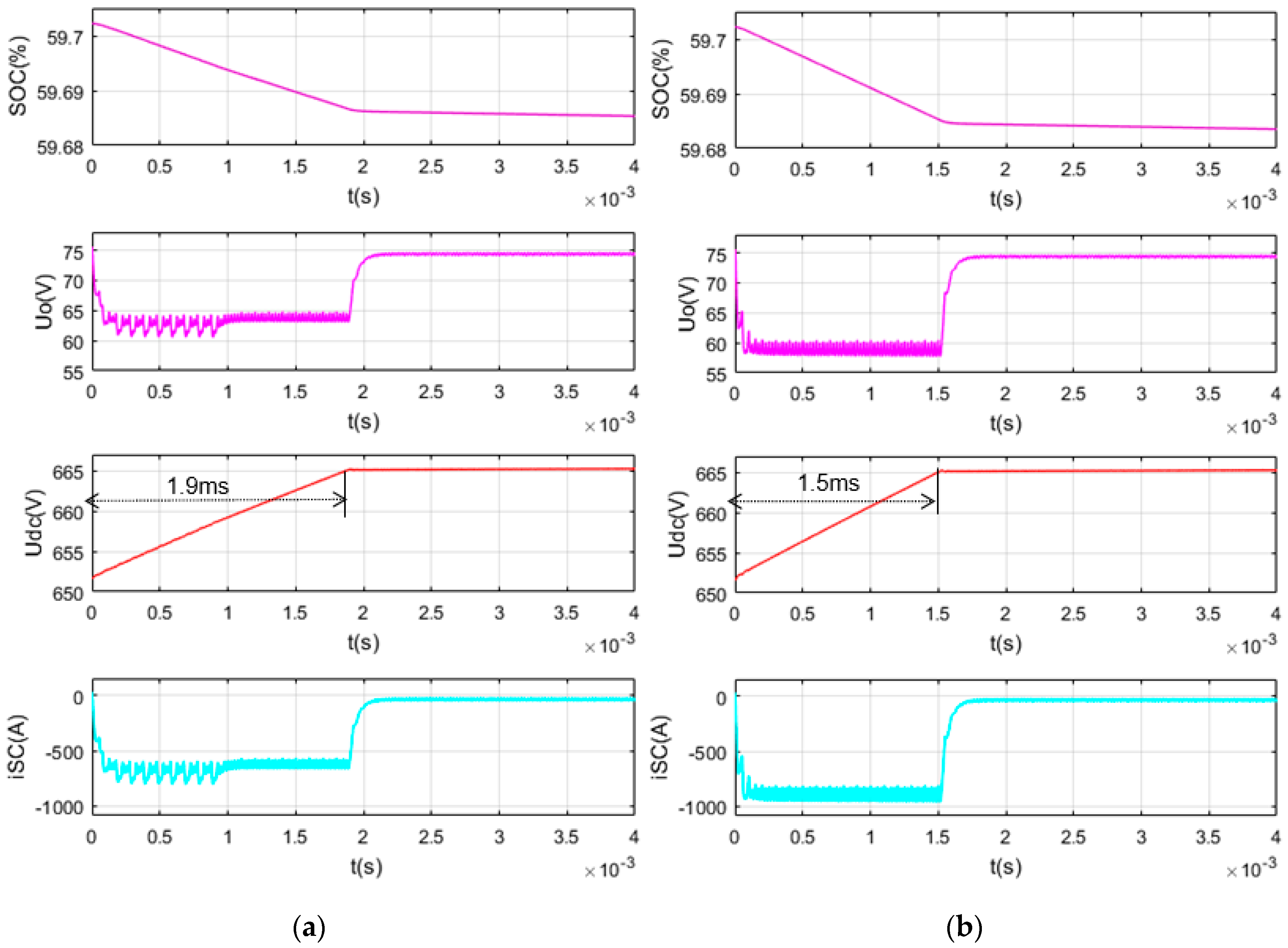
When the DC bus voltage, Udc, is lower than the lower limit voltage of 665 V, which is 651.7 V, and the initial value of the voltage, Uo, on the SC side is 75 V, the dynamic response time of the system is 1.9 ms when the bus voltage is stabilized to 665 V with only a prediction model of the DAB converter. The simulation waveform is shown in Figure 7a. Under the same conditions, using the overall prediction model composed of the DAB converter and the SC to control the SC discharge to stabilize the bus voltage to 665 V, the dynamic response time of the system is 1.5 ms, and the simulation waveform is shown in Figure 7b. Under these simulation conditions, a detailed waveform of the drive signal is shown in Figure A1 (see Appendix A).
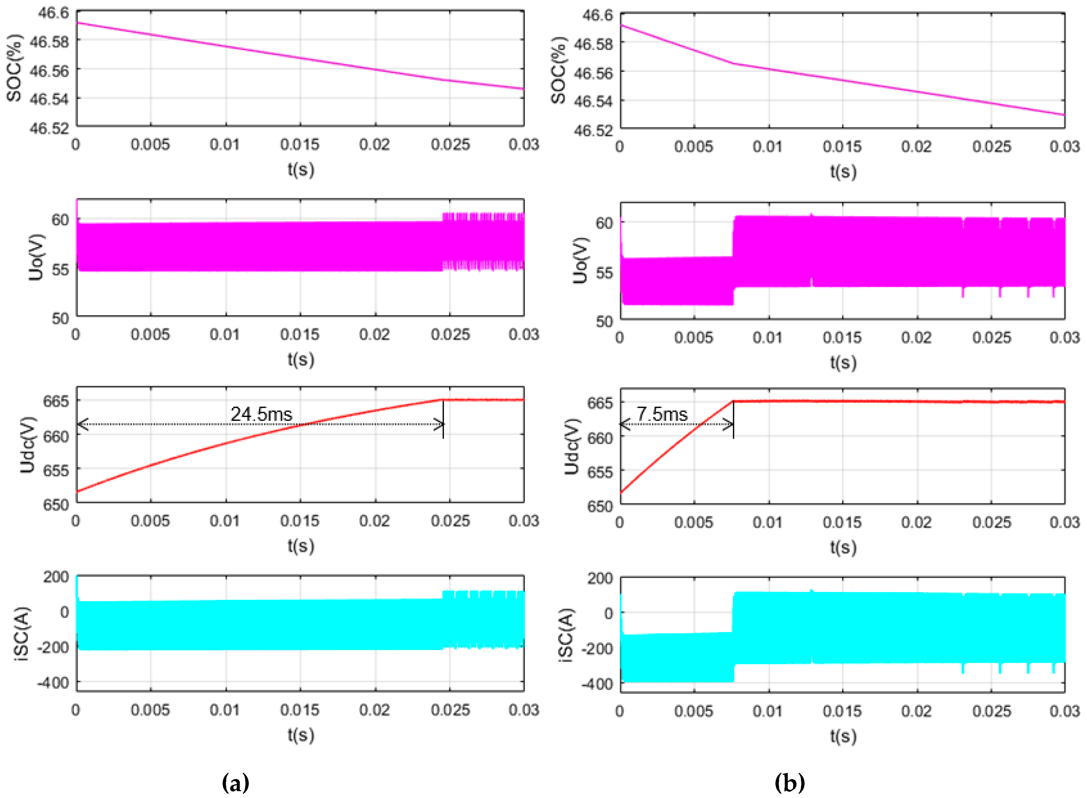
When the DC bus voltage, Udc, is lower than the lower limit voltage of 665 V, which is 651.7 V, and the initial value of the voltage, Uo, on the SC side is 58.6 V, the dynamic response time of the system is 24.5 ms when the bus voltage is stabilized to 665 V by using the DAB converter only to establish a prediction model to control the SC discharge. The simulation waveform is shown in Figure 8a. Under the same conditions, using the overall prediction model composed of the DAB converter and the SC to control the SC discharge to stabilize the bus voltage to 665 V, the dynamic response time of the system is 7.5 ms, and the simulation waveform is shown in Figure 8b.
It can be seen from the simulation results in Figure 7 and Figure 8 that when the SC is discharged from different SOCs, the method of using the overall model of the DAB converter and the SC for predictive control to stabilize the bus voltage always obtains faster response times than the method of using the MPC only for the DAB converter to stabilize the bus voltage.
5.2. SC Charge in the Normal Working Range
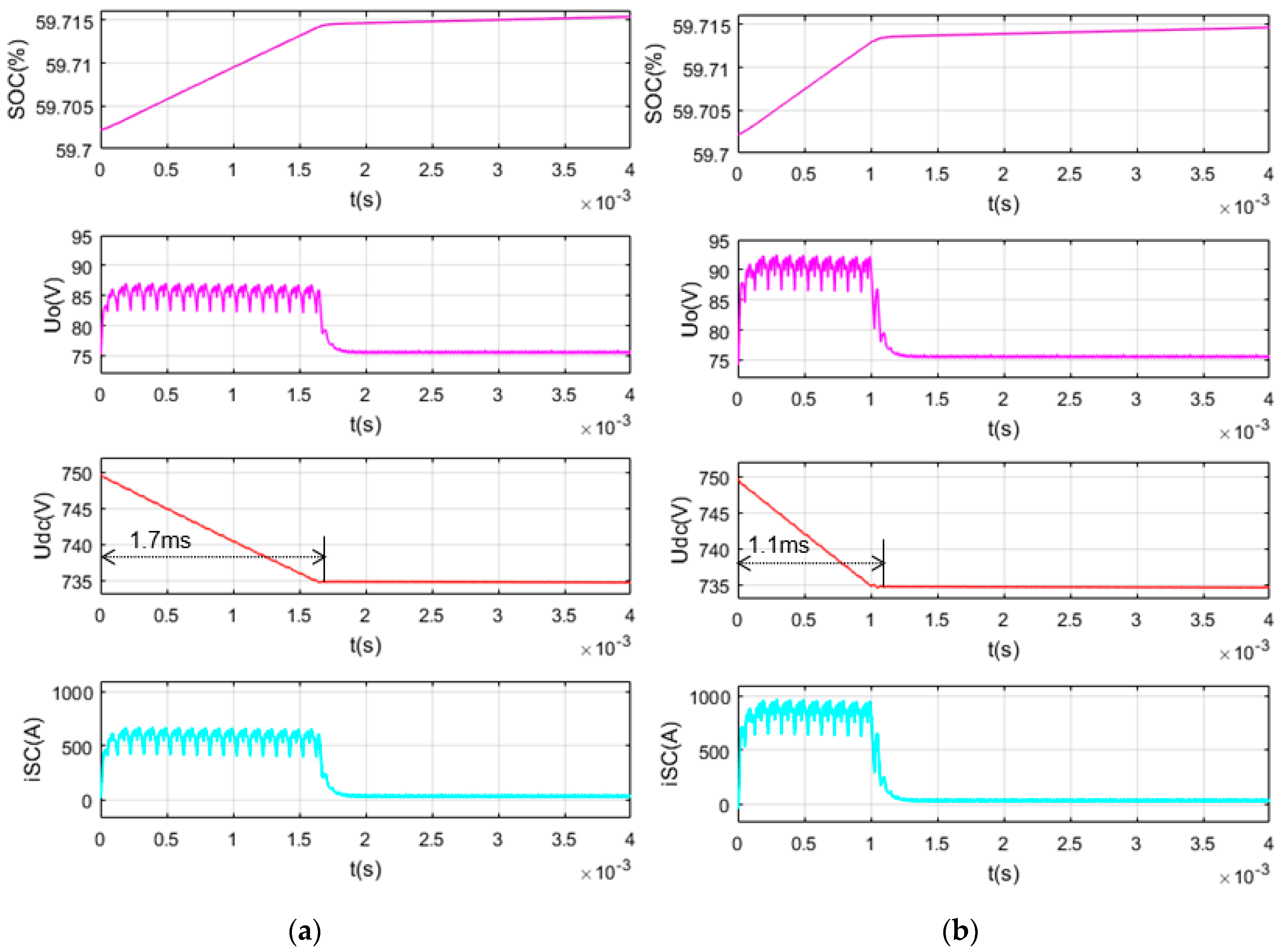
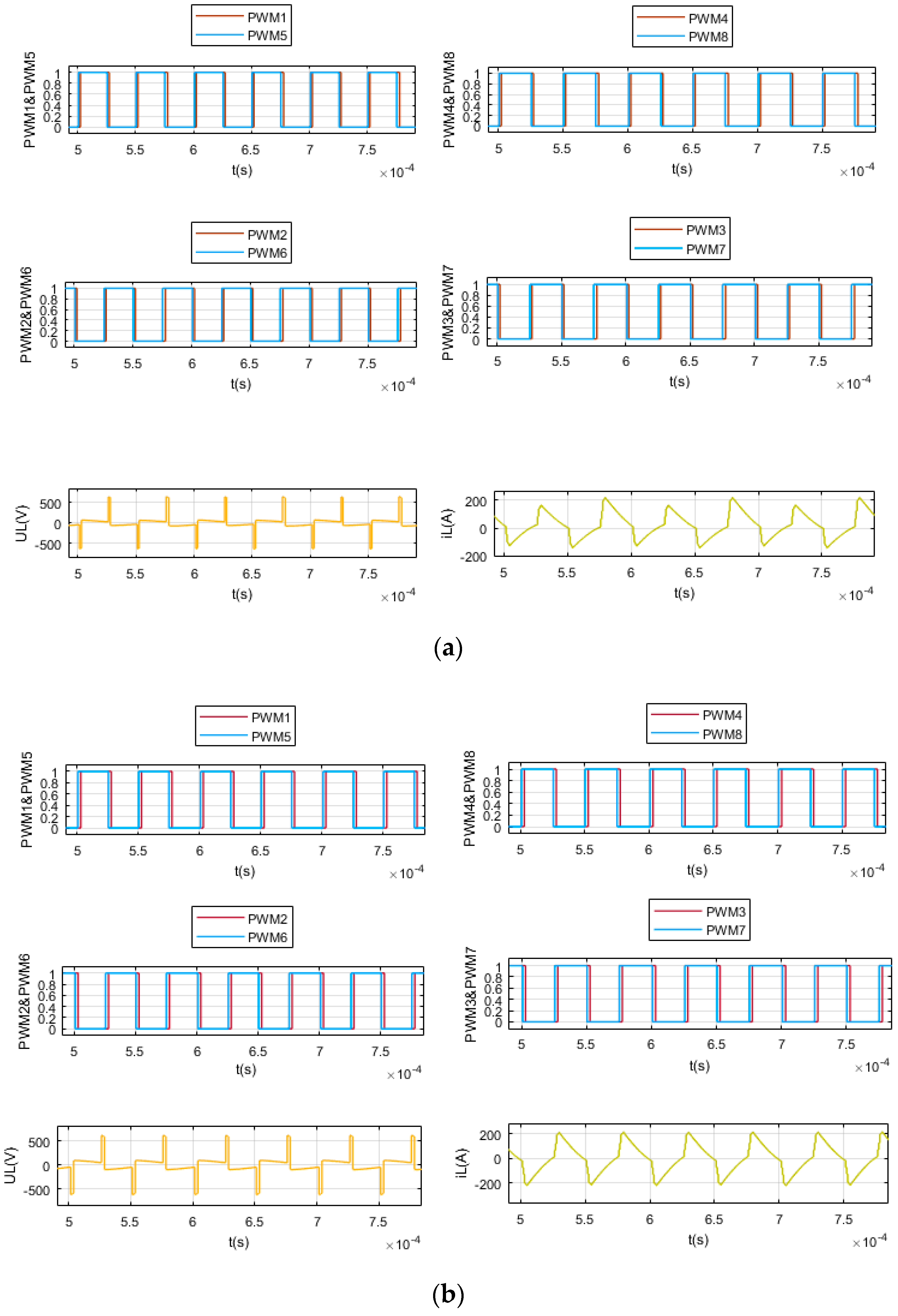
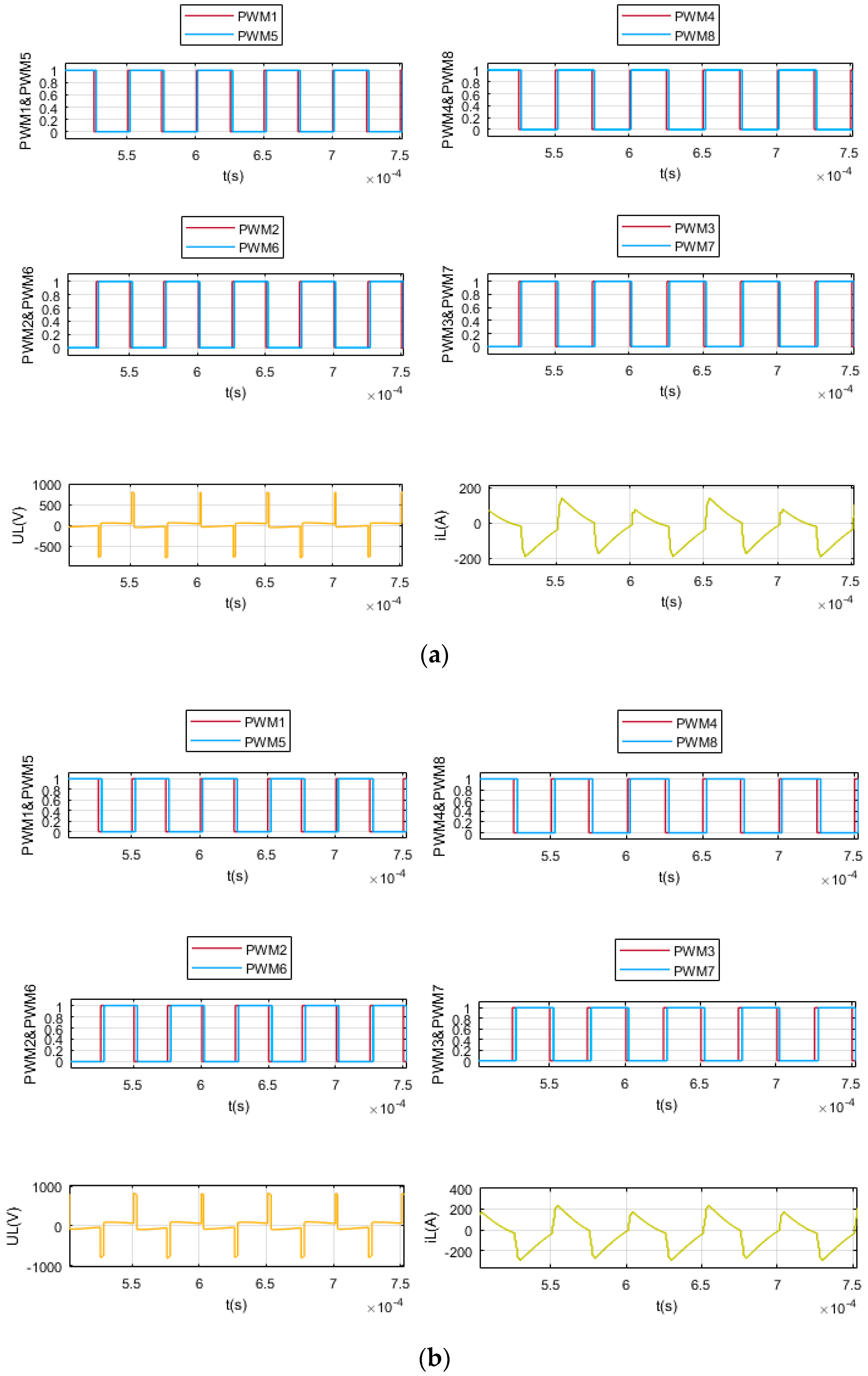
When the DC bus voltage, Udc, is higher than the higher limit voltage of 735 V, which is 749.7 V, and the initial value of the voltage, Uo, on the SC side is 75 V, the dynamic response time of the system is 1.7 ms when the bus voltage is stabilized to 735 V by using the DAB converter only to establish a prediction model to control the SC charge. The simulation waveform is shown in Figure 9a. Under the same conditions, using the overall prediction model composed of the DAB converter and the SC to control the SC charge to stabilize the bus voltage to 735 V, the dynamic response time of the system is 1.1 ms, and the simulation waveform is shown in Figure 9b. Under the simulation conditions, a detailed waveform of the drive signal is shown in Figure A2 (see Appendix B).
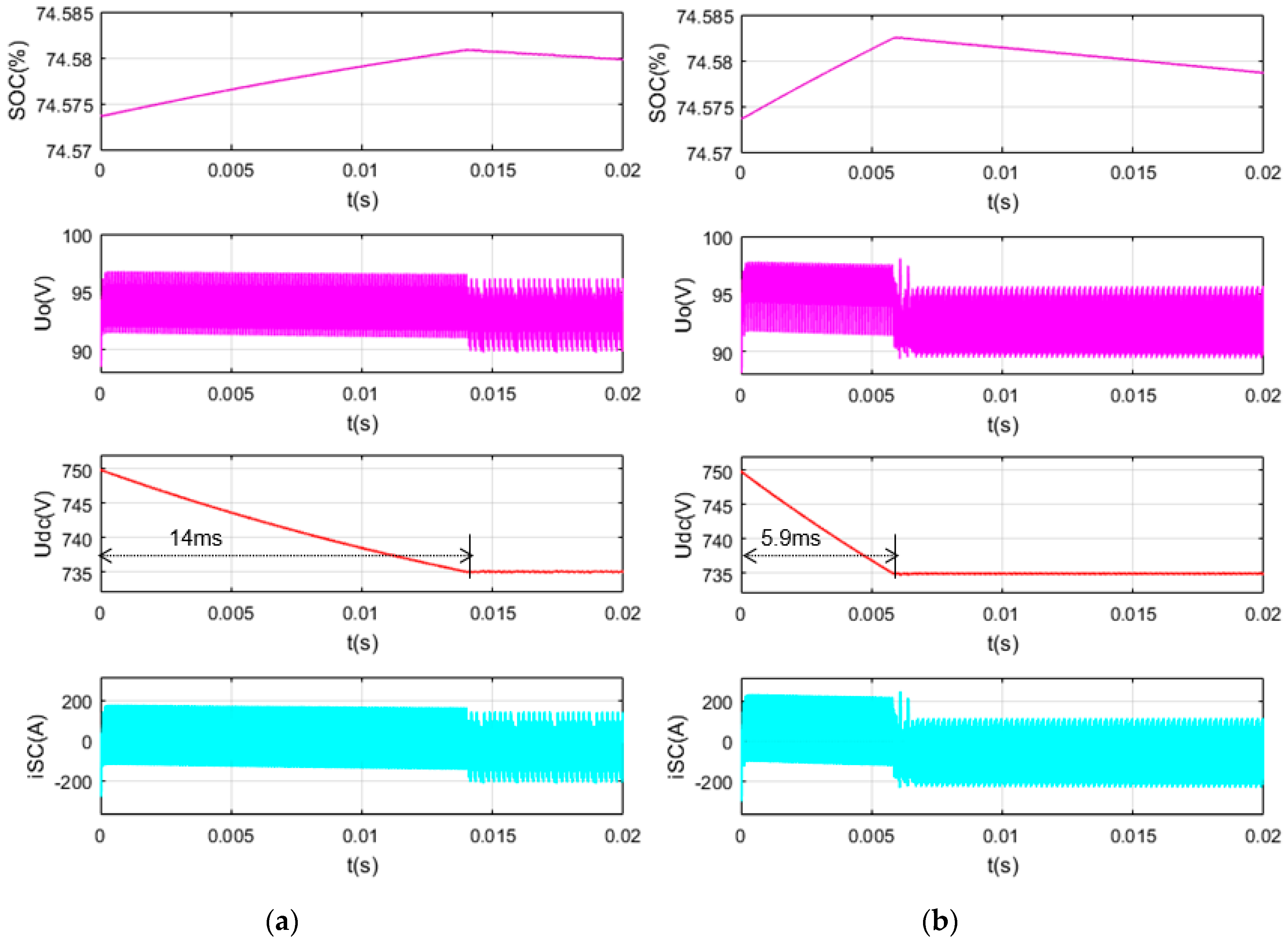
When the output power of the photovoltaic is high, the voltage, Udc, on the DC bus side is higher than the higher limit voltage of 735 V, which is 749.7 V, and the initial value of the voltage, Uo, on the SC side is 93.6 V, the dynamic response time of the system is 14 ms when the bus voltage is stabilized to 735 V by using the DAB converter only to establish a prediction model to control the SC charge. The simulation waveform is shown in Figure 10a. Under the same conditions, using the overall prediction model composed of the DAB converter and the SC to control the SC charge to stabilize the bus voltage to 735 V, the dynamic response time of the system is 5.9 ms, and the simulation waveform is shown in Figure 10b.
It can be seen from the simulation results in Figure 9 and Figure 10 that when the SC is charged from different SOCs, the method of using the overall model of the DAB converter and the SC for predictive control to stabilize the bus voltage always obtains faster response times than the method of using the MPC only for the DAB converter to stabilize the bus voltage.
5.3. SC Discharge Closer to the Lower Limit
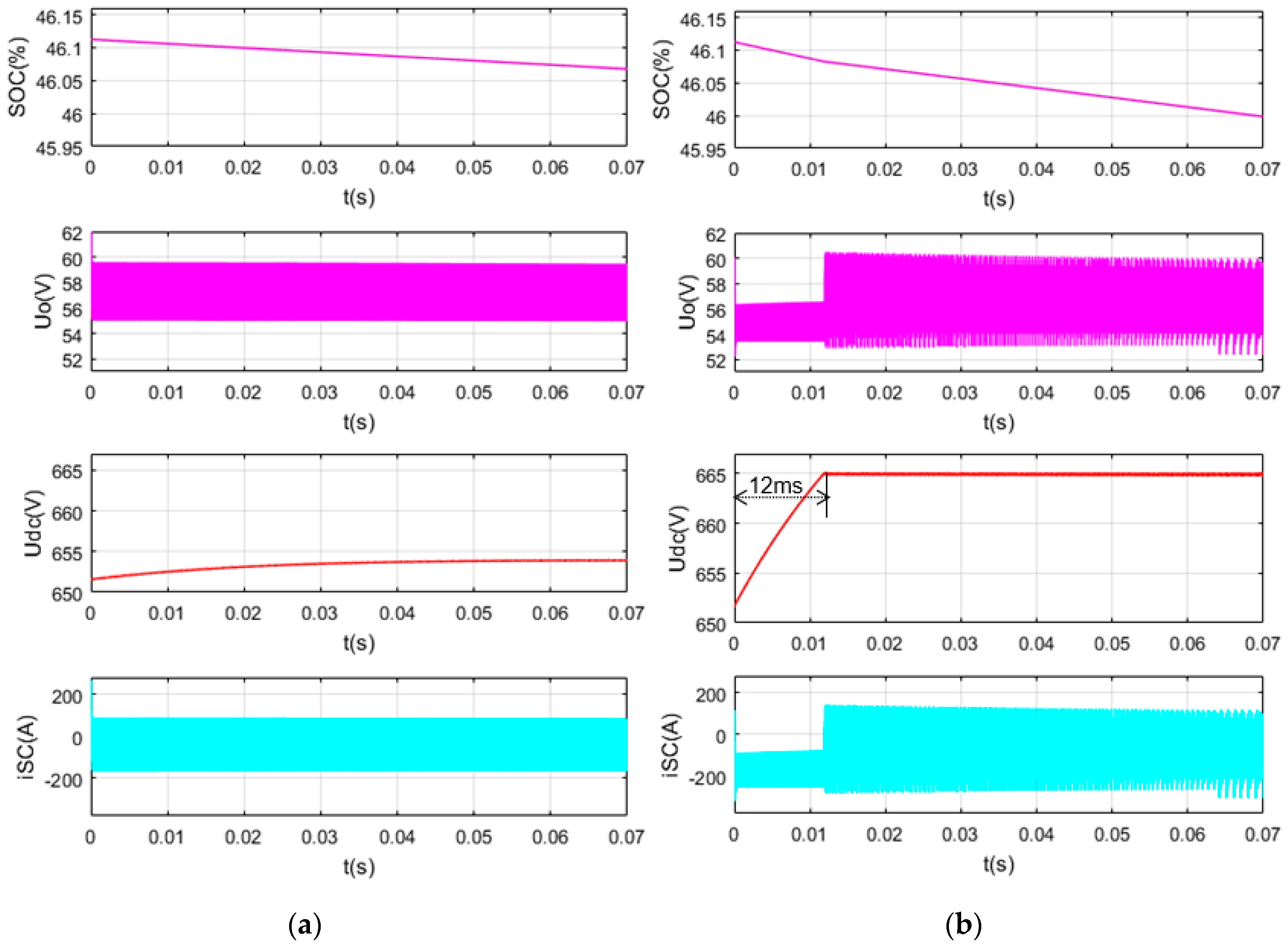
Through the observations of Figure 7, Figure 8, Figure 9 and Figure 10, it can be found that in these four cases, compared with the method of using the MPC only for the DAB converter to stabilize the bus voltage, the method of using the overall prediction model composed of the DAB converter and the SC to stabilize the bus voltage makes the SC voltage have a larger amount of change. Figure 11 contains the simulation waveforms obtained by using two different control methods when the voltage, Udc, on the DC bus side is 651.7 V and the initial value of the voltage, Uo, on the SC side is 58 V. As can be seen from Figure 11a, in this case, a method of establishing a prediction model only for the DAB converter to control the discharge of the SC cannot stabilize the bus voltage to 665 V. It can be seen from Figure 11b that the dynamic response time of the system is 12 ms by using the overall prediction model composed of the DAB converter and the SC to control the SC discharge to stabilize the bus voltage to 665 V.
When the voltage, Udc, on the DC bus side is 651.7 V, and the initial value of the voltage, Uo, on the SC side is 56.58 V, using the overall prediction model composed of the DAB converter and the SC to control the SC charge to stabilize the bus voltage to 665 V, the dynamic response time of the system is 15 ms, and the simulation waveform is shown in Figure 12.
5.4. SC Charge Closer to the Upper Limit
Figure 13 contains the simulation waveforms obtained by using two different control methods when the voltage, Udc, on the DC bus side is 749.7 V and the initial value of the voltage, Uo, on the SC side is 94 V. As can be seen from Figure 13a, in this case, the method of establishing a prediction model only for the DAB converter to control the charge of the SC cannot stabilize the bus voltage to 735 V. It can be seen from Figure 13b that the dynamic response time of the system is 6 ms by using the overall prediction model composed of the DAB converter and the SC to control the SC charge to stabilize the bus voltage to 735 V.
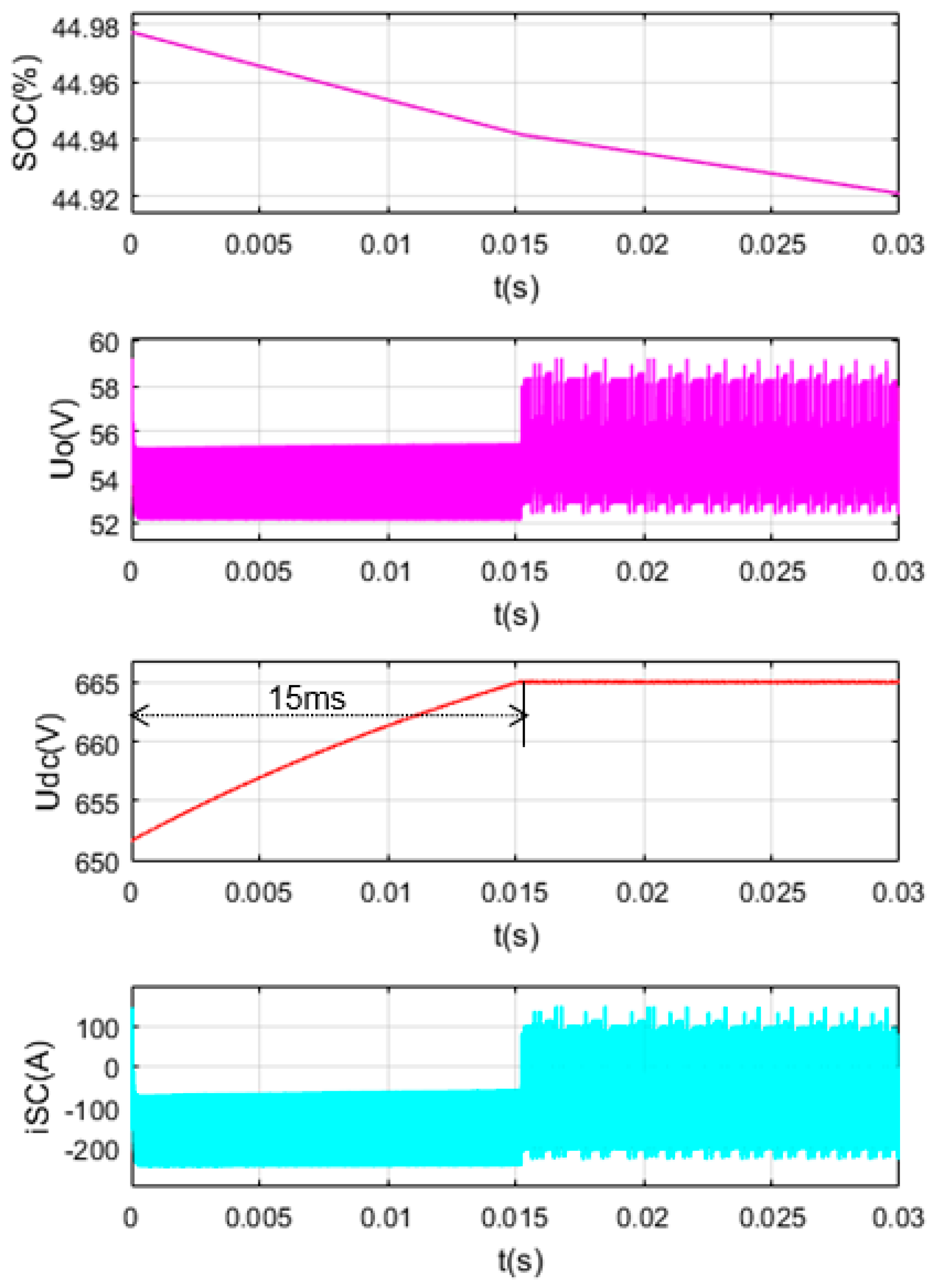
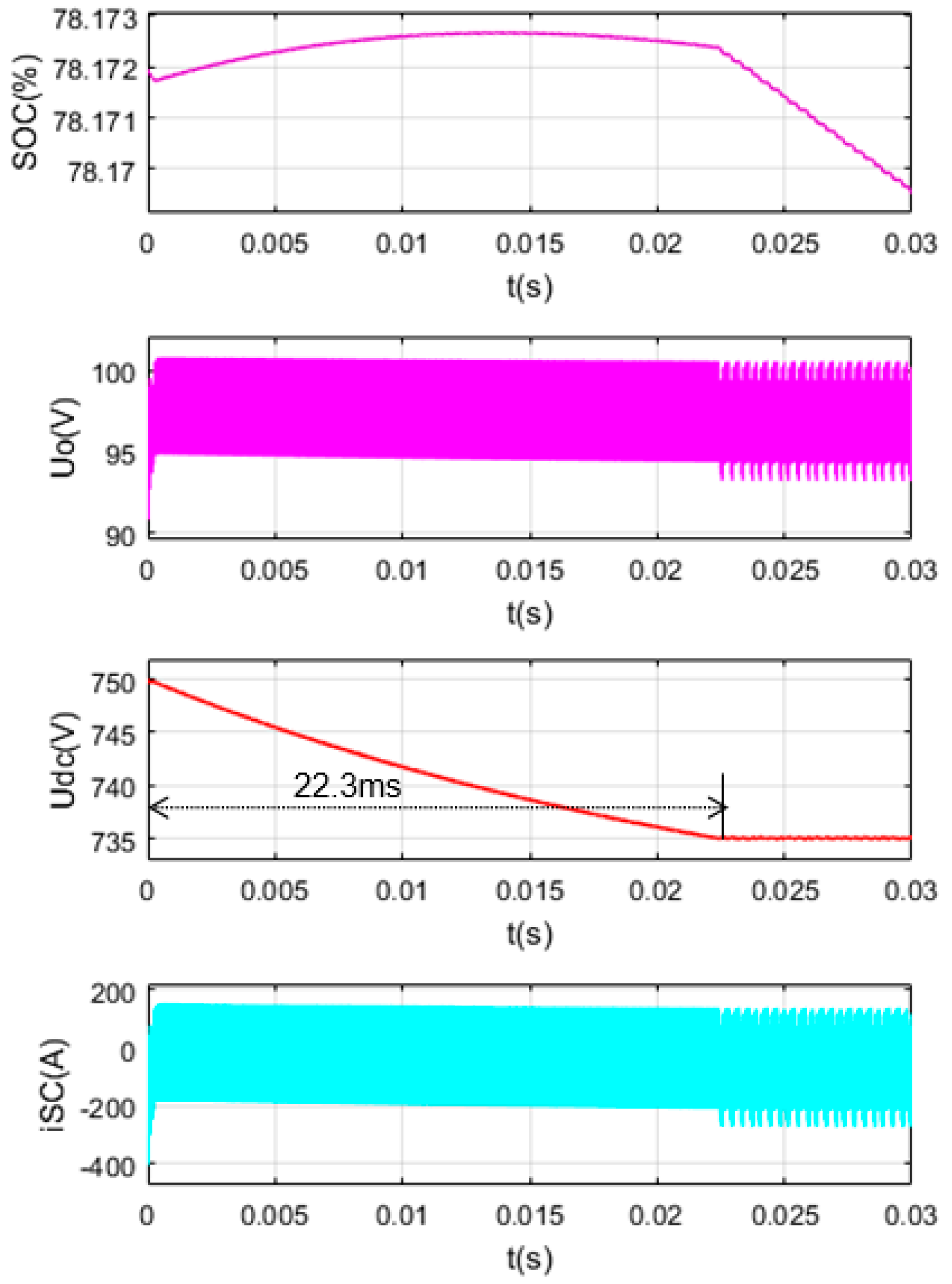
When the voltage, Udc, on the DC bus side is 749.7 V, and the initial value of the voltage, Uo, on the SC side is 98.1 V, using the overall prediction model composed of the DAB converter and the SC to control the SC charge to stabilize the bus voltage to 735 V, the dynamic response time of the system is 22.3 ms, and the simulation waveform is shown in Figure 14.
It can be seen from the simulation results of Figure 11, Figure 12, Figure 13 and Figure 14 that compared with the method of establishing a prediction model only for the DAB converter to stabilize the bus voltage, the method of using the overall prediction model composed of the DAB converter and the SC to stabilize the bus voltage increases the actual upper limit of the SC voltage, reduces the actual lower limit of the SC voltage, and expands the actual capacity utilization range of the SC by 18.63%.
6. Conclusions
In this paper, a hybrid MPC strategy composed of a DAB and SC was proposed in order to improve the dynamic characteristics of an energy storage system. The structural characteristics of the SCs were analyzed, and a suitable equivalent model of the SC was chosen for its fast response characteristics. The working principle of the DAB converter in each stage under single-phase shift control was analyzed and the prediction model of the DAB-SC system was established. By combining the SC model and the DAB model, an appropriate evaluation target was selected to establish the objective function for model prediction. A simulation model of the DAB-SC system was built in MATLAB/Simulink for verification. The simulation results show that the proposed method with the overall prediction model composed of a DAB converter and SC can effectively improve the overall response speed of the system and expand the actual capacity utilization range of the SC. The validity of the proposed method was verified and the proposed method has good application prospects in improving the dynamic response performance of energy storage systems.
Author Contributions
Conceptualization, J.G. and L.W.; methodology, J.G.; software, J.G.; validation, J.G., L.W. and T.W.; formal analysis, C.X.; investigation, H.L.; resources, C.X.; data curation, J.G.; writing—original draft preparation, J.G.; writing—review and editing, J.G. and L.W.; visualization, J.G.; supervision, L.W.; project administration, T.W.; funding acquisition, L.W.
Funding
This research was funded by National Natural Science Foundation Youth Project of China, grant number 51607060.
Conflicts of Interest
The authors declare no conflict of interest.
Abbreviation
| SC | Supercapacitor |
| DAB | Dual active bridge |
| RC | Resistor-capacitor |
| ANN | Artificial neural network |
| DC | Direct current |
| ZVS | Zero voltage switch |
| AC | Alternative current |
| MPC | Model predictive control |
| SOC | State of charge |
Appendix A
It can be seen from Figure A1 that the secondary side drive signal of the converter leads the primary side drive signal in SC discharge state. And comparing Figure A1a and Figure A1b, it can be seen that compared with the method of establishing a prediction model only for the DAB converter to control SC discharge, the method of controlling SC discharge by using the overall prediction model composed of the DAB converter and SC has a larger amplitude of inductor current, and due to the internal resistance RES of SC, the voltage on the low voltage side declines instantaneously when SC is discharged, making Udc > nUo, therefore, the inductor current in the power transfer mode of the converter decreases linearly when SC is discharged.
Figure A1.
Detailed simulation waveform diagram of the drive signal when Udc initial voltage is 651.7 V and Uo initial voltage is 75 V: (a) MPC only for DAB; (b) MPC for DAB-SC system.
Figure A1.
Detailed simulation waveform diagram of the drive signal when Udc initial voltage is 651.7 V and Uo initial voltage is 75 V: (a) MPC only for DAB; (b) MPC for DAB-SC system.

Appendix B
It can be seen from Figure A2 that the primary side drive signal of the converter leads the secondary side drive signal in SC discharge state. And comparing Figure A2a and Figure A2b, it can be seen that compared with the method of establishing a prediction model only for the DAB converter to control SC discharge, the method of controlling SC discharge by using the overall prediction model composed of the DAB converter and SC has a larger amplitude of the inductor current, and due to the internal resistance RES of SC, the voltage on the low voltage side rises instantaneously when SC is charged, making Udc < nUo, therefore, the inductor current in the power transfer mode of the converter decreases linearly when SC is charged.
Figure A2.
Detailed Simulation waveform diagram of the drive signal when Udc initial voltage is 749.7 V and Uo initial voltage is 75 V: (a) MPC only for DAB; (b) MPC for DAB-SC system.
Figure A2.
Detailed Simulation waveform diagram of the drive signal when Udc initial voltage is 749.7 V and Uo initial voltage is 75 V: (a) MPC only for DAB; (b) MPC for DAB-SC system.

References
- Liu, J.; Zhang, L. Strategy Design of Hybrid Energy Storage System for Smoothing Wind Power Fluctuations. Energies 2016, 9, 991. [Google Scholar] [CrossRef]
- Wang, L. Research of Converter Topology Based on Super Capacitor Energy Storage System. Electron. Des. Eng. 2018, 26, 29–133. [Google Scholar]
- Xun, Q.; Wang, P.; Quan, L.; Xu, Y. Voltage Balancing Strategy Based on Cooperative Control for Super Capacitor. Power Electron. 2017, 51, 113–116. [Google Scholar]
- Han, W.; Huang, S.; Dai, Q.; Wan, J. Modeling and Simulation of an Elevator Energy-saving System Based on Isolated Bidirectional DC/DC Converter. Electr. Autom. 2015, 37, 7–9. [Google Scholar]
- Lv, X.; Liu, C.; Wang, Y.; Li, Z. Research of Bidirectional DC-DC Converter in Distributed Wind-photovoltaic-storage System. Electr. Meas. Instrum. 2017, 54, 16–20, 41. [Google Scholar]
- Choi, W.; Rho, K.M.; Cho, B.H. Fundamental Duty Modulation of Dual-Active-Bridge Converter for Wide Range Operation. IEEE Trans. Power Electron. 2016, 31, 4048–4064. [Google Scholar] [CrossRef]
- Sha, D.; Wang, X.; Chen, D. High Efficiency Current-Fed DAB DC–DC Converter with ZVS Achievement throughout Full Range of Load Using Optimized Switching Patterns. IEEE Trans. Power Electron. 2018, 33, 1347–1357. [Google Scholar] [CrossRef]
- Takagi, K.; Fujita, H. Dynamic Control and Performance of a Dual-Active-Bridge DC-DC Converter. IEEE Trans. Power Electron. 2018, 33, 7858–7866. [Google Scholar] [CrossRef]
- Yi, L.; Chen, Y.; Zhang, H.; Guo, Z. Unified Control for Mode Swap of Bidirectional DC/DC Converter in Distributed Generation System. Power Electron. 2017, 51, 4–7. [Google Scholar]
- Oggier, G.; Ordonez, M.; Galvez, J.; Luchino, F. Fast Transient Boundary Control and Steady-state Operation of the DAB Converter Using the Natural Switching Surface. IEEE Trans. Power Electron. 2014, 29, 946–957. [Google Scholar] [CrossRef]
- Hou, N.; Song, W.; Wu, M. A Load Current Feedforward Control Scheme of DAB DC/DC Converters. Proc. Csee 2016, 36, 2478–2485. [Google Scholar]
- Song, W.; Hou, N.; Wu, M. Virtual Direct Power Control Scheme of DAB DC-DC Converters for Fast Dynamic Response. IEEE Trans. Power Electron. 2018, 33, 1750–1759. [Google Scholar] [CrossRef]
- Yang, K.; Song, W.; An, F.; Hou, N. Rapid Dynamic Response Control Method of Dual-active-bridge DC-DC Converters in Current Source Mode. Proc. Csee 2018, 38, 2439–2447, S23. [Google Scholar]
- An, F.; Song, W.; Yang, K. Model Predictive Control and Power Balance Scheme of Dual-active-bridge DC-DC Converters in Power Electronic Transformer. Proc. Csee 2018, 38, 3921–3929, S22. [Google Scholar]
- Wang, X.; Han, M.; Gao, F.; Wang, M.; Wang, K. A Review of Modeling in New Energy Research on Super-capacitor. World Power Supply 2016, 1, 37–40, S28. [Google Scholar]
- Yu, P.; Jing, T.; Yang, R. Capacitance Measurement and Parameter Estimation Method for SCs with Variable Capacitance. Trans. Chin. Soc. Agric. Eng. 2016, 32, 169–174. [Google Scholar]
- Hu, B.; Yang, Z.; Lin, F.; Zhao, K.; Zhao, Y. Equivalent Circuit Model of Super Capacitor Group for Urban Rail Transit Application. Electr. Drive Locomot. 2013, 5, 65–68, 74. [Google Scholar]
- Feng, J.; Xu, F.; Li, L.; Qin, Y.; Shi, X. Capacitance Measurement of SCs Based on Discharge Procedure with Constant Load. Electron. Compon. Mater. 2016, 35, 88–91. [Google Scholar]
- Yuan, X. A Research on Phase-shift-control of the Full-bridge-isolated DC/DC Converter. Electr. Autom. 2017, 39, 7–10. [Google Scholar]
- Kan, J.; Wu, Y.; Xie, S.; Tang, Y.; Xue, Y.; Yao, Z.; Zhang, B. Dual-active-bridge Bidirectional DC/DC Converter Based on High-frequency AC Buck-Boost Theory. Proc. Csee 2017, 37, 1797–1807, S24. [Google Scholar]
- Xue, Y.; Zhou, J.; Cui, Y. Simulation Research on Coordinated Control Strategy of Hybrid Energy Storage Based on DC Microgrid. Electr. Mach. Control Appl. 2017, 44, 19–25, 37. [Google Scholar]
Figure 1.
Simplified capacitor circuit model of the SC unit.

Figure 2.
Topology of the DAB-SC system.

Figure 3.
The main working waveform of the DAB converter with phase shift control: (a) Forward power transfer; (b) reverse power transfer.
Figure 3.
The main working waveform of the DAB converter with phase shift control: (a) Forward power transfer; (b) reverse power transfer.

Figure 4.
Schematic diagram of the MPC strategy.

Figure 5.
MPC structure block diagram.

Figure 6.
Simulation model of the DAB-SC system based on Matlab/Simulink: (a) The overall model; (b) model of the DAB converter.
Figure 6.
Simulation model of the DAB-SC system based on Matlab/Simulink: (a) The overall model; (b) model of the DAB converter.


Figure 7.
Simulation waveform diagram when the initial voltage, Udc, is 651.7 V and the initial voltage, Uo, is 75 V: (a) MPC only for the DAB; (b) MPC for the DAB-SC system.
Figure 7.
Simulation waveform diagram when the initial voltage, Udc, is 651.7 V and the initial voltage, Uo, is 75 V: (a) MPC only for the DAB; (b) MPC for the DAB-SC system.

Figure 8.
Simulation waveform diagram when the initial voltage, Udc, is 651.7 V and the initial voltage, Uo, is 58.6 V: (a) MPC only for the DAB; (b) MPC for the DAB-SC system.
Figure 8.
Simulation waveform diagram when the initial voltage, Udc, is 651.7 V and the initial voltage, Uo, is 58.6 V: (a) MPC only for the DAB; (b) MPC for the DAB-SC system.

Figure 9.
Simulation waveform diagram when the initial voltage, Udc, is 749.7 V and the initial voltage, Uo, is 75 V: (a) MPC only for the DAB; (b) MPC for the DAB-SC system.
Figure 9.
Simulation waveform diagram when the initial voltage, Udc, is 749.7 V and the initial voltage, Uo, is 75 V: (a) MPC only for the DAB; (b) MPC for the DAB-SC system.

Figure 10.
Simulation waveform diagram when the initial voltage, Udc, is 749.7 V and the initial voltage, Uo, is 93.6 V: (a) MPC only for the DAB; (b) MPC for the DAB-SC system.
Figure 10.
Simulation waveform diagram when the initial voltage, Udc, is 749.7 V and the initial voltage, Uo, is 93.6 V: (a) MPC only for the DAB; (b) MPC for the DAB-SC system.

Figure 11.
Simulation waveform diagram when the initial voltage, Udc, is 651.7 V and the initial voltage, Uo, is 58 V: (a) MPC only for the DAB; (b) MPC for the DAB-SC system.
Figure 11.
Simulation waveform diagram when the initial voltage, Udc, is 651.7 V and the initial voltage, Uo, is 58 V: (a) MPC only for the DAB; (b) MPC for the DAB-SC system.

Figure 12.
Simulation waveform diagram of the MPC for the DAB-SC system when the initial voltage, Udc, is 651.7 V and the initial voltage, Uo, is 56.58 V.
Figure 12.
Simulation waveform diagram of the MPC for the DAB-SC system when the initial voltage, Udc, is 651.7 V and the initial voltage, Uo, is 56.58 V.

Figure 13.
Experimental waveform diagram when the initial voltage, Udc, is 749.7 V and the initial voltage, Uo, is 94 V: (a) MPC only for the DAB; (b) MPC for the DAB-SC system.
Figure 13.
Experimental waveform diagram when the initial voltage, Udc, is 749.7 V and the initial voltage, Uo, is 94 V: (a) MPC only for the DAB; (b) MPC for the DAB-SC system.

Figure 14.
Simulation waveform diagram of the MPC for the DAB-SC system when the initial voltage, Udc, is 749.7 V and the initial voltage, uo, is 98.1 V.
Figure 14.
Simulation waveform diagram of the MPC for the DAB-SC system when the initial voltage, Udc, is 749.7 V and the initial voltage, uo, is 98.1 V.


Table 1.
Simulation Parameters.
| Symbol | Quantity |
|---|---|
| fs | 20 kHz |
| Udc | 700 V |
| C | 3 × 10⁻³ F |
| L | 6.815 × 10⁻⁶ H |
| n | 9 |
| RES | 0.018 Ω |
| Kv | 0.1127 |
| C0 | 81.384 |
© 2019 by the authors. Licensee MDPI, Basel, Switzerland. This article is an open access article distributed under the terms and conditions of the Creative Commons Attribution (CC BY) license (http://creativecommons.org/licenses/by/4.0/).
Share and Cite
MDPI and ACS Style
Wang, L.; Guo, J.; Xu, C.; Wu, T.; Lin, H. Hybrid Model Predictive Control Strategy of Supercapacitor Energy Storage System Based on Double Active Bridge. Energies 2019, 12, 2134. https://doi.org/10.3390/en12112134
AMA Style
Wang L, Guo J, Xu C, Wu T, Lin H. Hybrid Model Predictive Control Strategy of Supercapacitor Energy Storage System Based on Double Active Bridge. Energies. 2019; 12(11):2134. https://doi.org/10.3390/en12112134
Chicago/Turabian StyleWang, Lujun, Jiong Guo, Chen Xu, Tiezhou Wu, and Huipin Lin. 2019. "Hybrid Model Predictive Control Strategy of Supercapacitor Energy Storage System Based on Double Active Bridge" Energies 12, no. 11: 2134. https://doi.org/10.3390/en12112134
Note that from the first issue of 2016, this journal uses article numbers instead of page numbers. See further details here.