Current Mode Control of a Series LC Converter Supporting Constant Current, Constant Voltage (CCCV)

 ,
,
Abstract
:1. Introduction
2. State-of-the-art
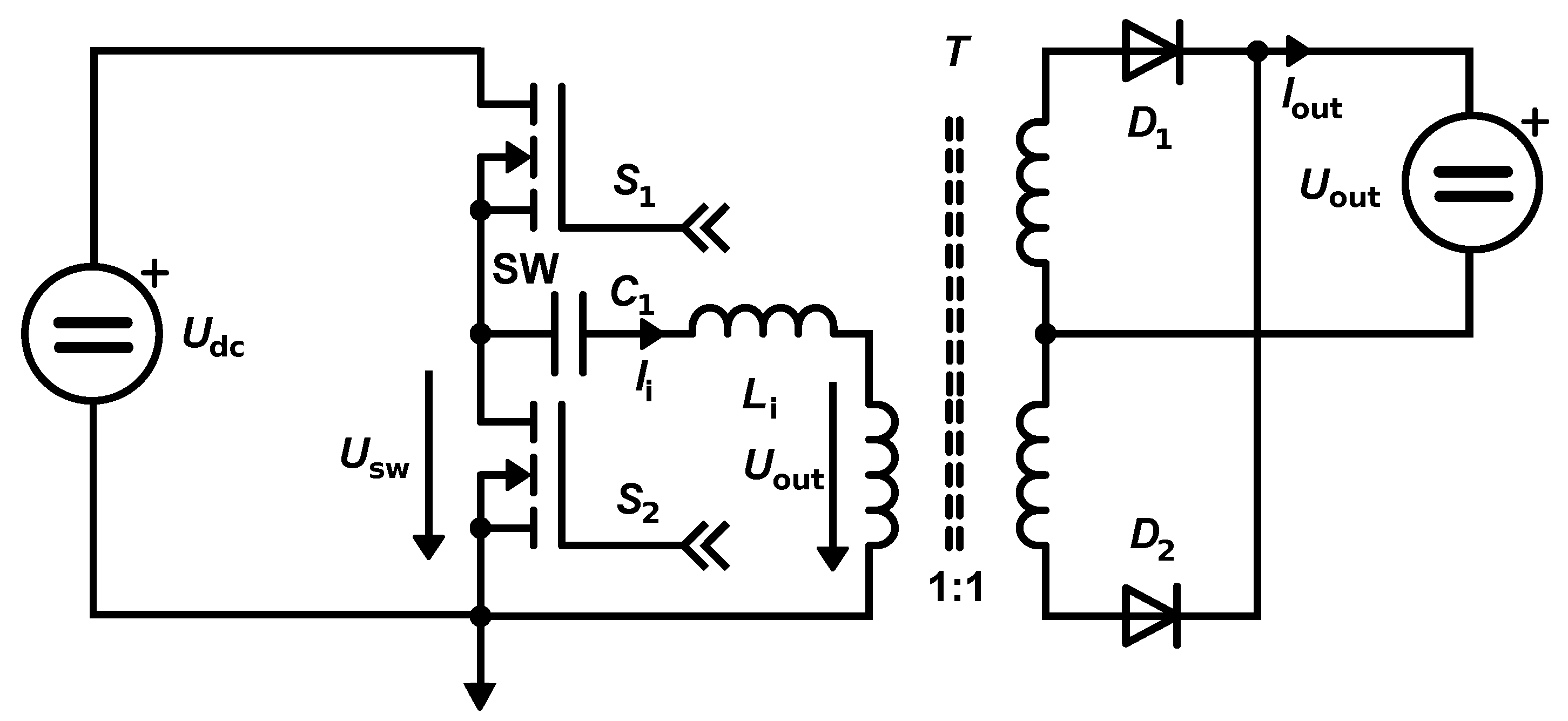
3. Fundamentals
4. Master Voltage Mode Controller
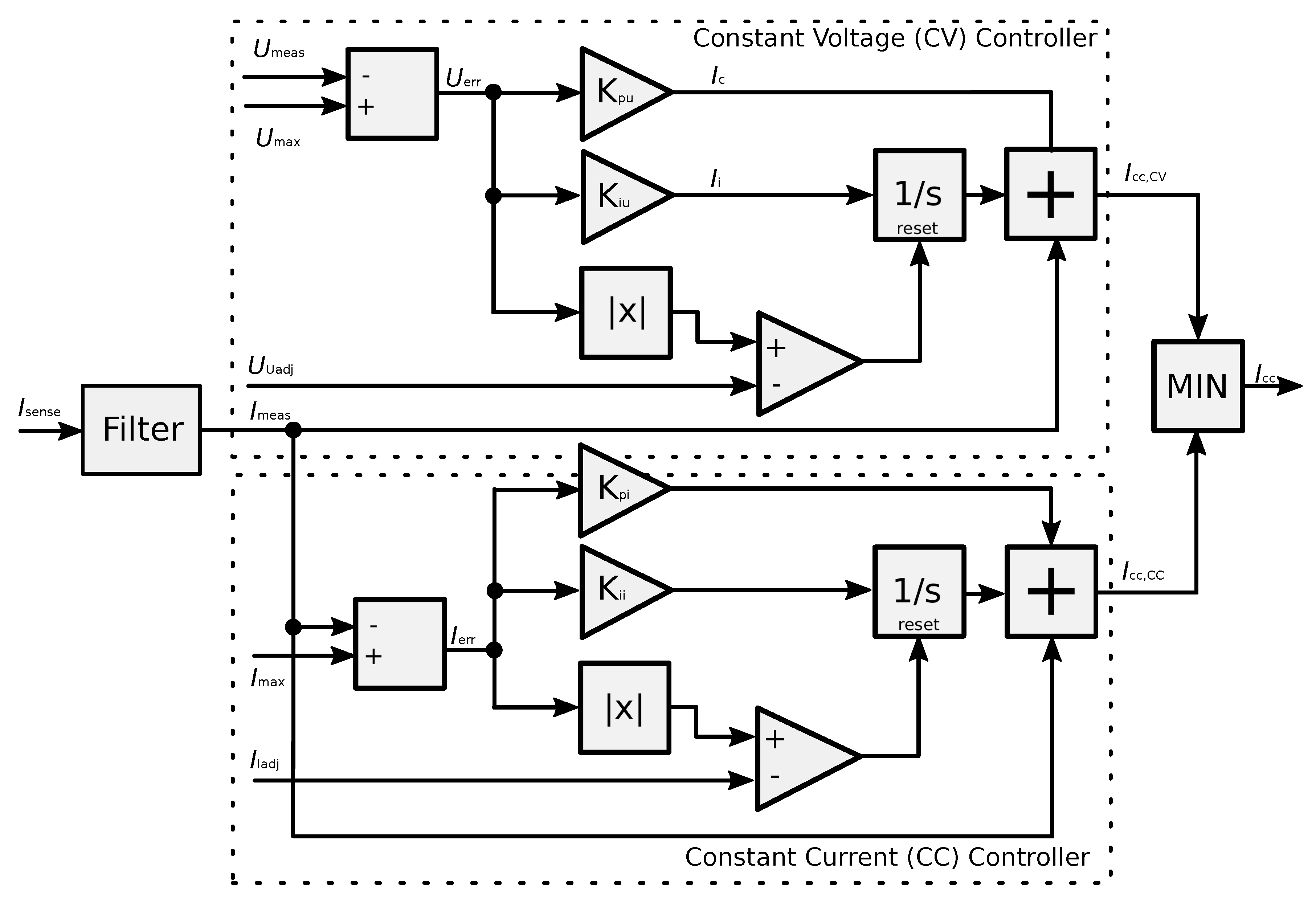
4.1. Constant Voltage Controller
4.2. Constant Current Controller
4.3. Acoustic Noise
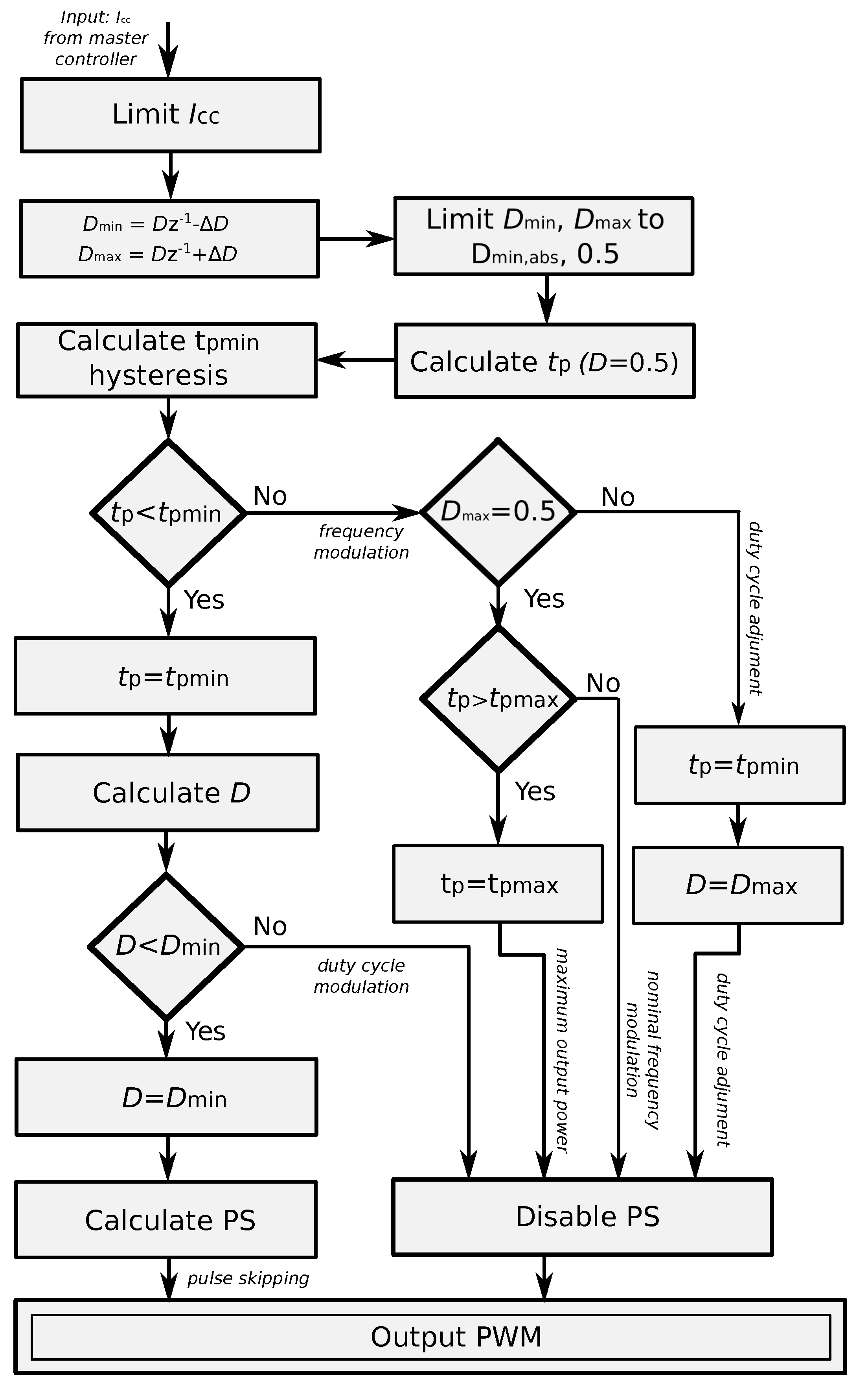
5. Slave Current Controller
5.1. Initial Calculus
5.2. Frequency Modulation
5.3. Duty Cycle Modulation
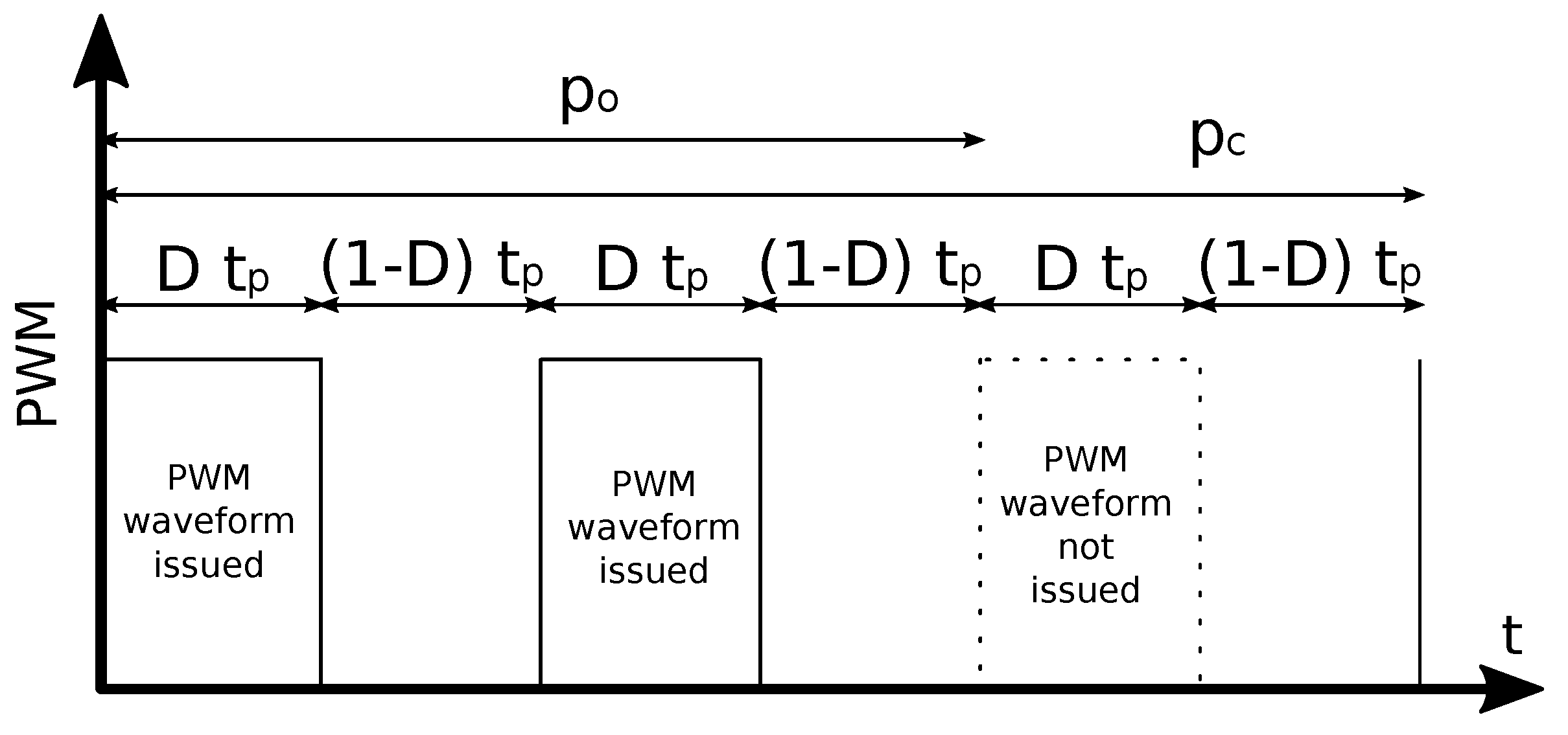
5.4. Pulse Skipping
5.5. Voltage Stress on
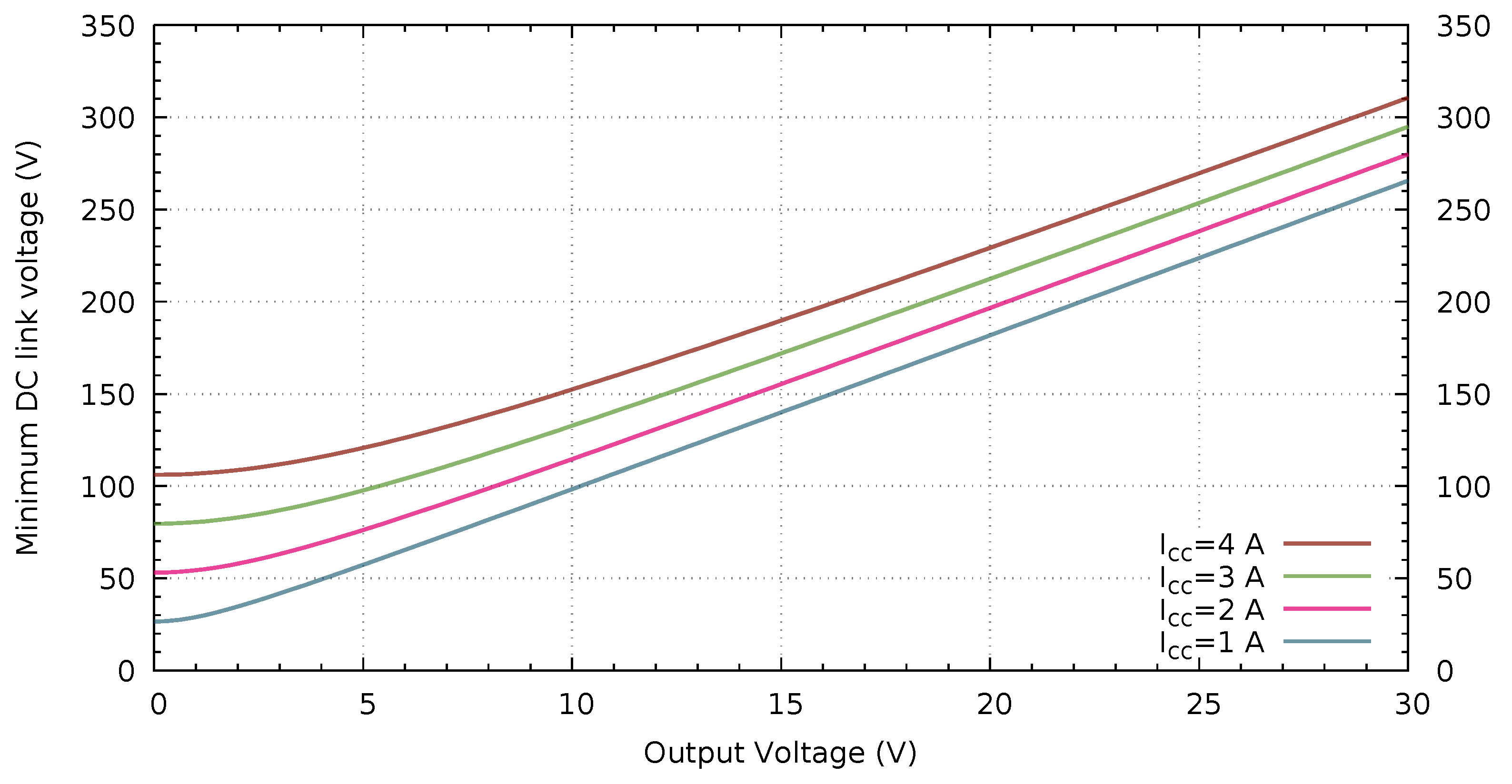
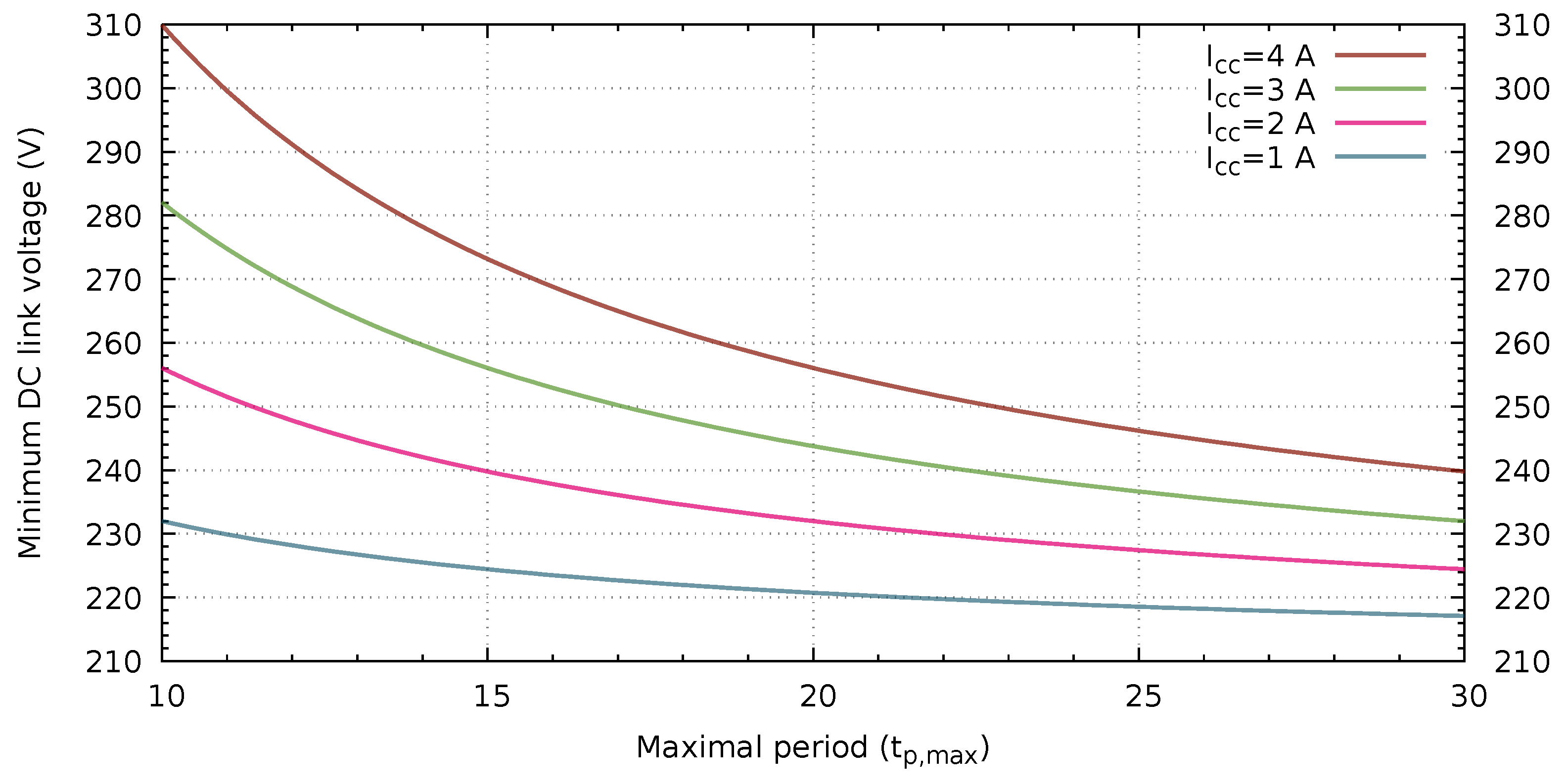
5.6. Input Voltage Range
6. Modulator
7. Simulation and Experimental Results
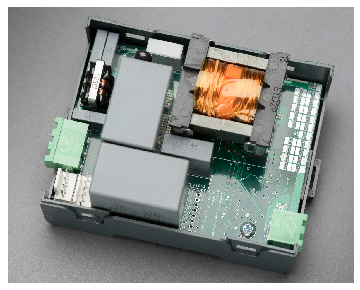
7.1. Measurement Setup
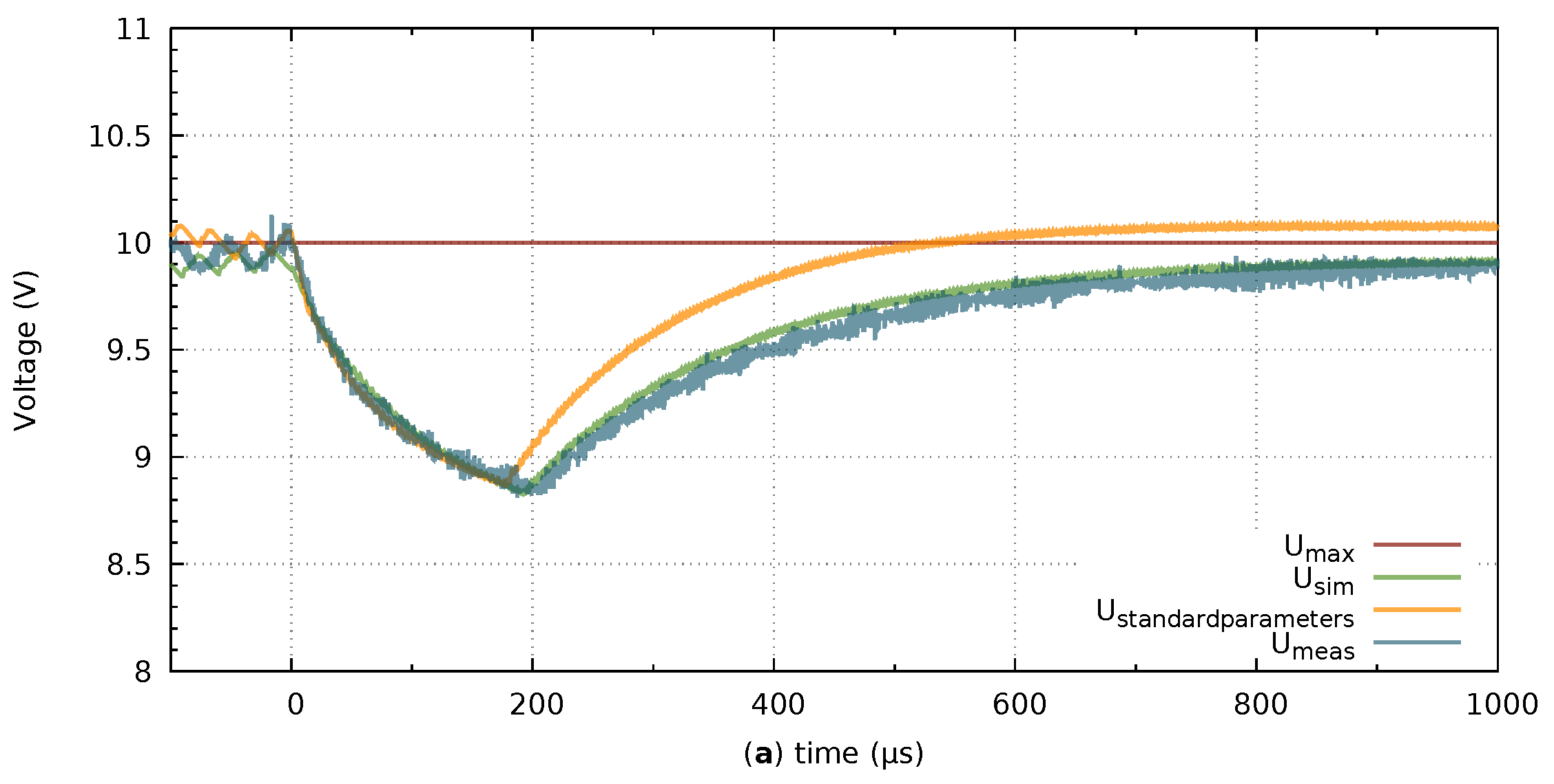
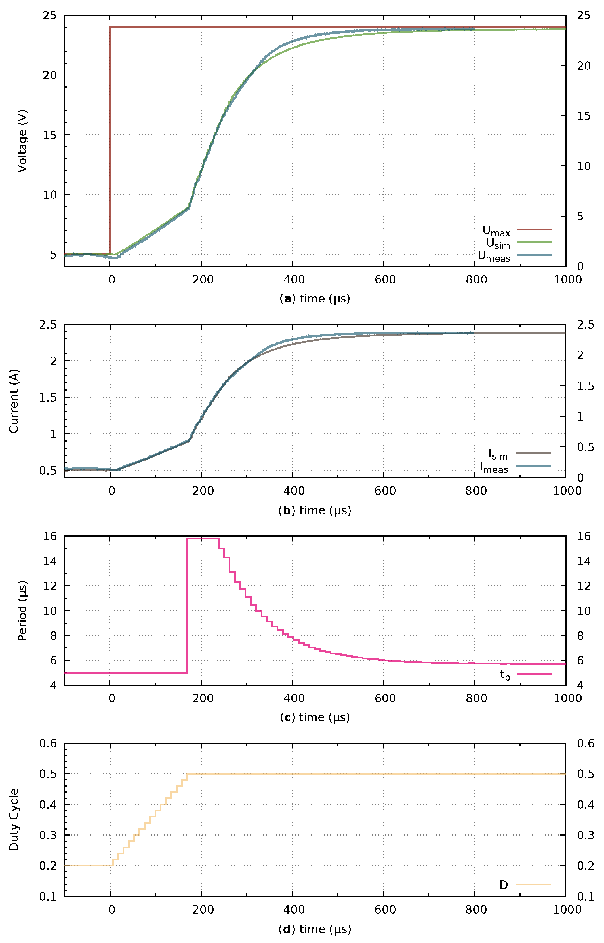
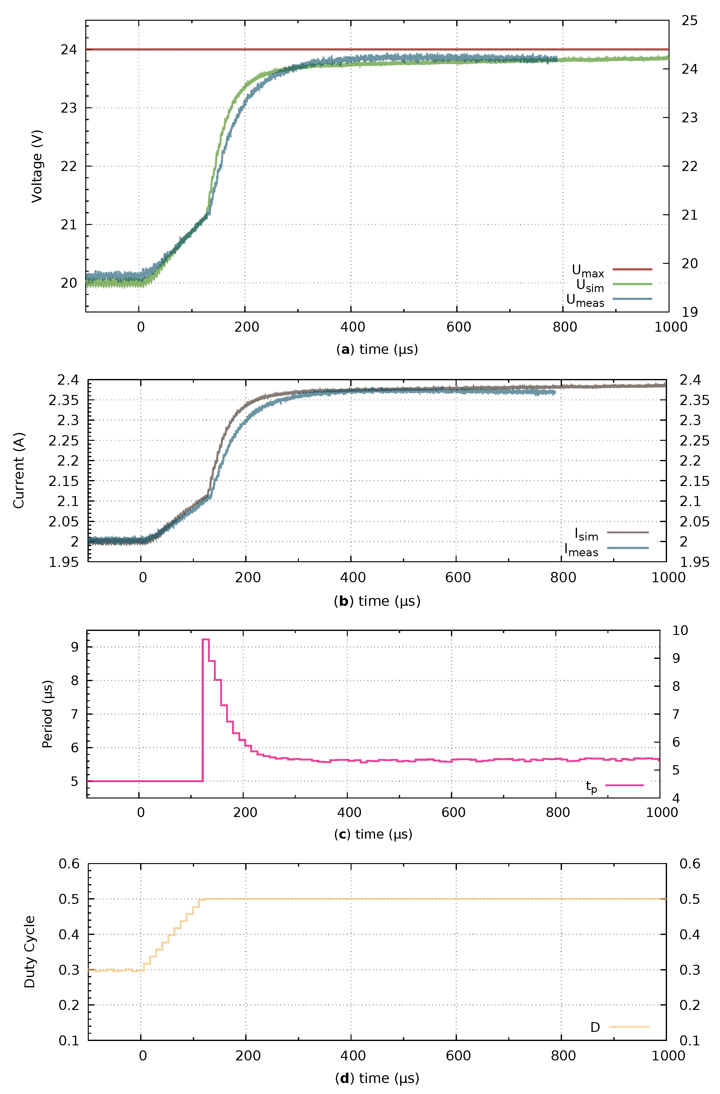
7.2. Voltage Step Response
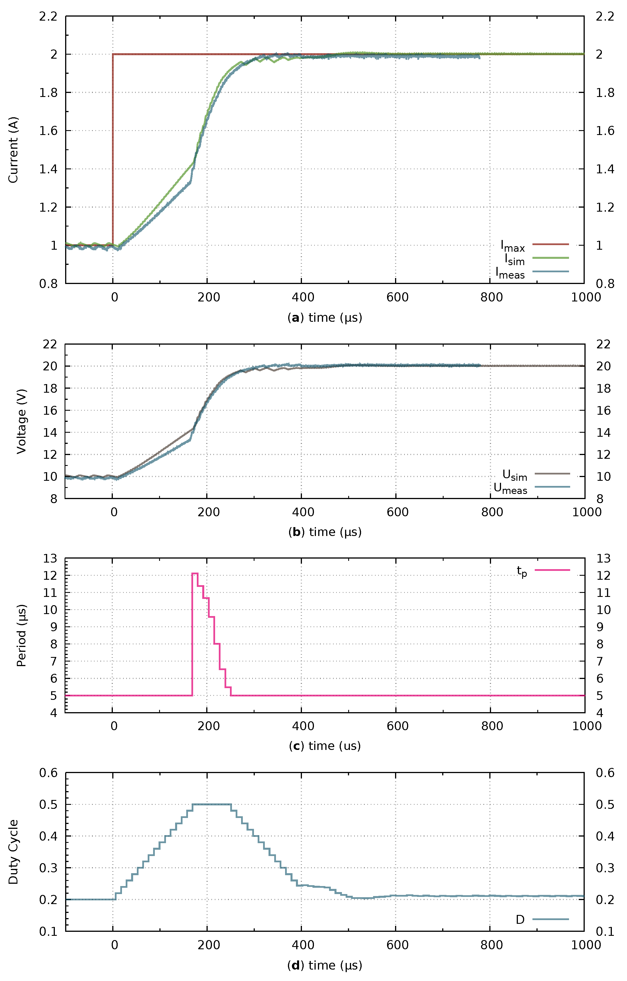
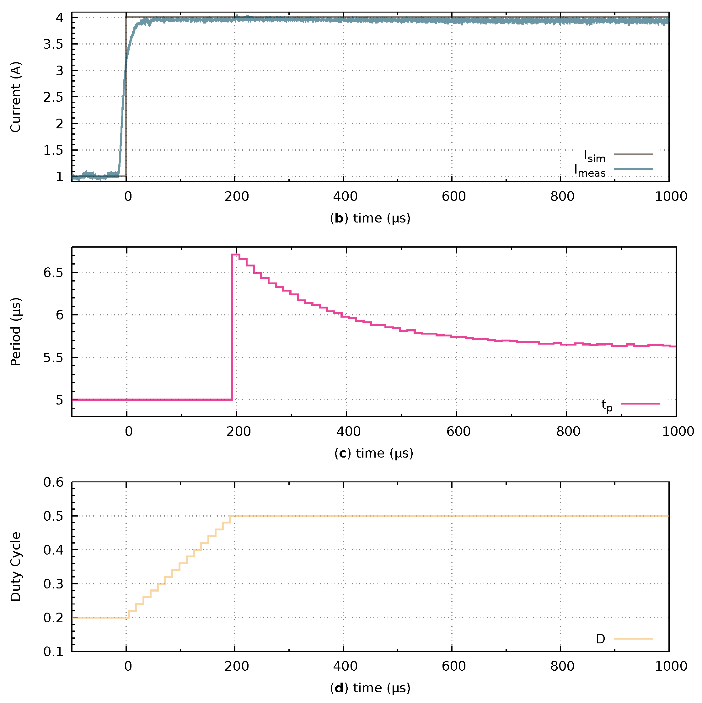
7.3. Current Step Response
7.4. Load Response
7.5. CCCV Transition Step Response
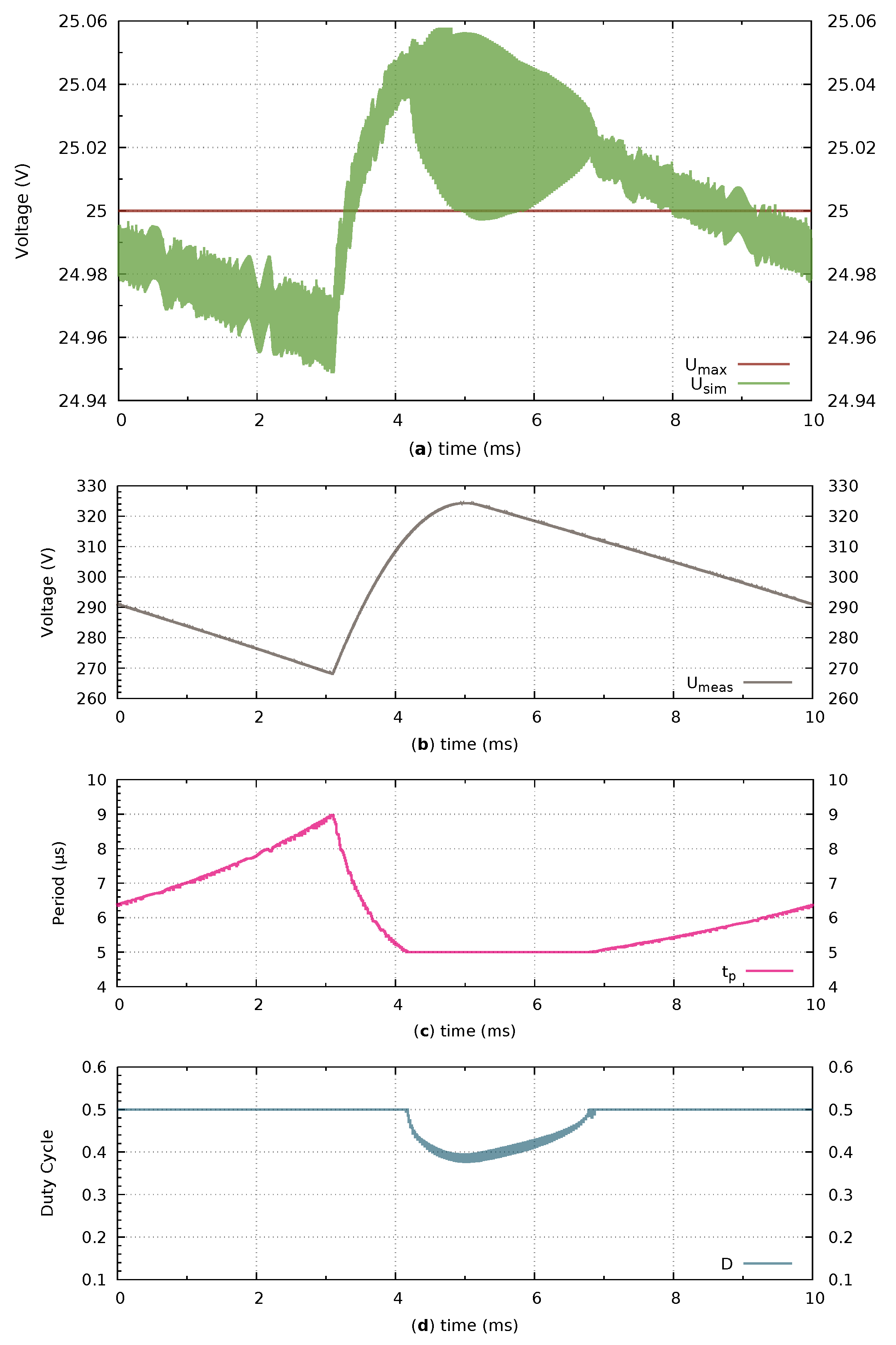
7.6. AC Input Voltage Range
7.7. DC Link Ripple Rejection
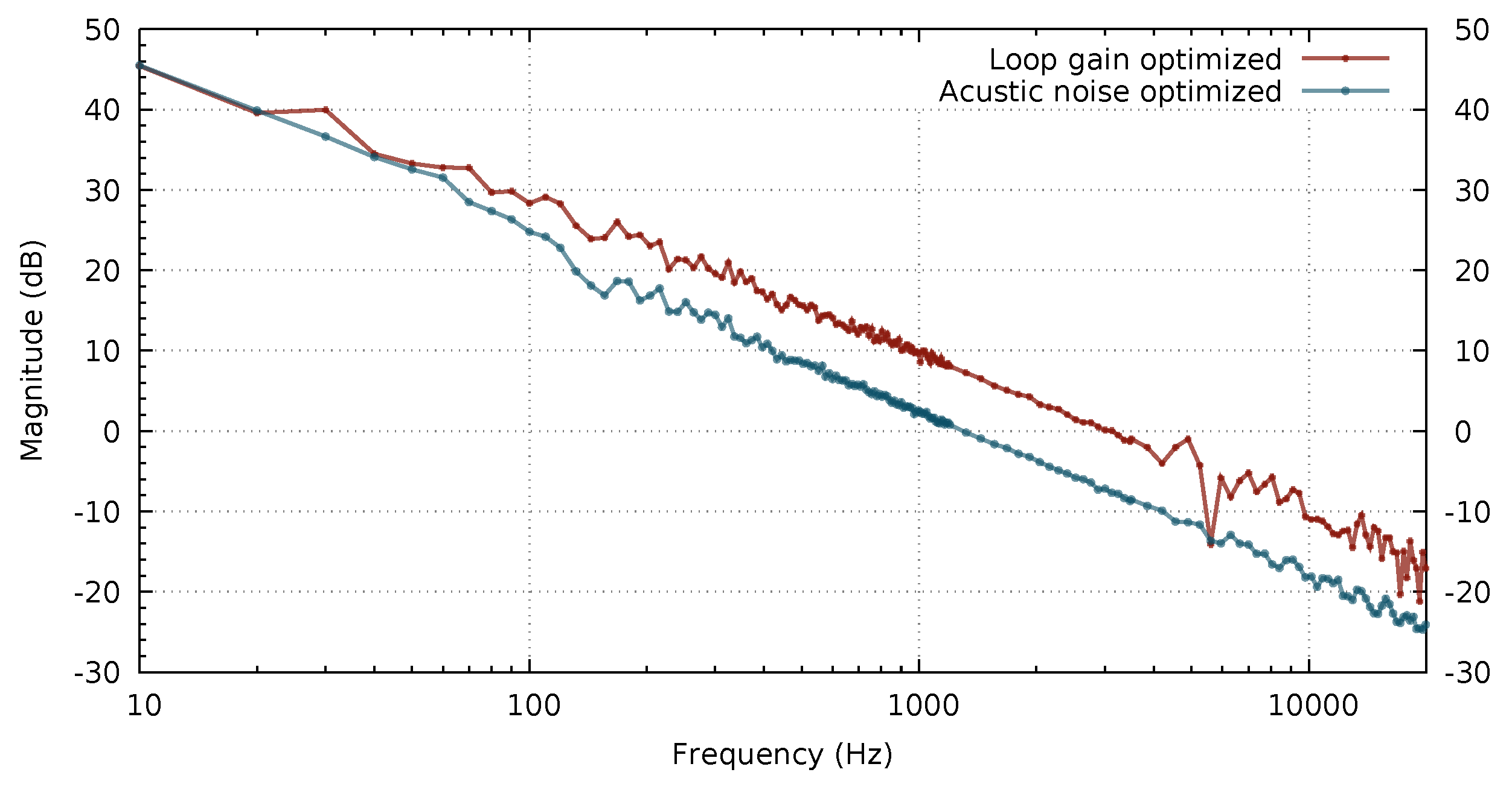
7.8. Loop Gain Analysis
8. Comparison with the State-of-the-art
8.1. Output Voltage Range
8.2. Input Voltage Range
8.3. DC Link Ripple Attenuation
8.4. Control Bandwidth
8.5. Overshoot
8.6. Large Signal Step Response
9. Conclusions
10. Patents
Author Contributions
Funding
Conflicts of Interest
Abbreviations
| CC | Constant current |
| CCCV | Constant current, constant voltage |
| CV | Constant voltage |
| DSP | Digital signal processor |
| MLCC | Multilayer ceramic capacitor |
| PT1 | First-order lag element |
| PT2 | Second-order lag element |
| PWM | Pulse width modulation |
| SMPS | Switch mode power supply |
| SL | Series LC (inductor capacitor) |
| SLCC | Series LC (inductor capacitor) converter |
References
- Heidinger, M.; Simon, C.; Fabian, D.; Eziguerre, S.; Heering, W. Open Loop Current Control of a Series LC Converter by Duty Cycle and Frequency. EPE J. 2018. submitted. [Google Scholar]
- Tissières, M.; Askarian, I.; Pahlevani, M.; Rotzetta, A.; Knight, A.; Preda, I. A digital robust control scheme for dual Half-Bridge DC-DC converters. In Proceedings of the 2018 IEEE Applied Power Electronics Conference and Exposition (APEC), San Antonio, TX, USA, 4–8 March 2018; pp. 311–315. [Google Scholar] [CrossRef]
- Liu, T.; Zhou, Z.; Xiong, A.; Zeng, J.; Ying, J. A Novel Precise Design Method for LLC Series Resonant Converter. In Proceedings of the INTELEC 06—Twenty-Eighth International Telecommunications Energy Conference, Providence, RI, USA, 10–14 September 2006; pp. 1–6. [Google Scholar] [CrossRef]
- Patarau, T.; Petreus, D.; Duma, R.; Dobra, P. Comparison between analog and digital control of LLC converter. In Proceedings of the 2010 IEEE International Conference on Automation, Quality and Testing, Robotics (AQTR), Cluj-Napoca, Romania, 28–30 May 2010; pp. 1–6. [Google Scholar] [CrossRef]
- Zhuang, M.; Atherton, D.P. Optimum cascade PID controller design for SISO systems. In Proceedings of the 1994 International Conference on Control—Control ’94, Coventry, UK, 21–24 March 1994; Volume 1, pp. 606–611. [Google Scholar] [CrossRef]
- Petkov, R.; Anguelov, G. Current mode control of frequency controlled resonant converters. In Proceedings of the INTELEC—Twentieth International Telecommunications Energy Conference (Cat. No.98CH36263), San Francisco, CA, USA, 4–8 October 1998; pp. 103–108. [Google Scholar] [CrossRef]
- Aizpuru, I.; Iraola, U.; Canales, J.M.; Echeverria, M.; Gil, I. Passive balancing design for Li-ion battery packs based on single cell experimental tests for a CCCV charging mode. In Proceedings of the 2013 International Conference on Clean Electrical Power (ICCEP), Alghero, Italy, 11–13 June 2013; pp. 93–98. [Google Scholar] [CrossRef]
- Kleebchampee, W.; Bunlaksananusorn, C. Modeling and Control Design of a Current-Mode Controlled Flyback Converter with Optocoupler Feedback. In Proceedings of the 2005 International Conference on Power Electronics and Drives Systems, Kuala Lumpur, Malaysia, 28 November–1 December 2005; pp. 787–792. [Google Scholar] [CrossRef]
- Fariborz, M.; Marian, C.; Deepak, G.; Wilson, E. Control Strategies for Wide Output Voltage Range LLC Resonant DC–DC Converters in Battery Chargers. IEEE Trans. Veh. Technol. 2014, 63, 1117–1125. [Google Scholar] [CrossRef]
- Brañas, C.; Azcondo, F.J.; Casanueva, R. Feedforward compensation of resonant converters with heavy ripple in the DC bus for LED lamp driver applications. In Proceedings of the 2013 IEEE 14th Workshop on Control and Modeling for Power Electronics (COMPEL), Salt Lake City, UT, USA, 23–26 June 2013; pp. 1–6. [Google Scholar] [CrossRef]
- Graham, R.L.; Knuth, D.E.; Patashnik, O. Concrete Mathematics: A Foundation for Computer Science, 2nd ed.; Addison-Wesley: Boston, UK, 1989; ISBN 0-201-55802-5. Available online: https://www.csie.ntu.edu.tw/~r97002/temp/Concrete%20Mathematics%202e.pdf (accessed on 15 July 2019).
- Texas Instruments Application Report: Ripple Rejection in AC/DC Systems Using LLC SLUA850. Available online: http://www.ti.com/lit/an/slua850/slua850.pdf (accessed on 15 July 2019).
- Texas Instruments. 600-W, Isolated PFC Power Supply for AVR Amplifiers Based on the TAS5630 and TAS5631. Available online: http://www.ti.com/lit/ug/slou293c/slou293c.pdf (accessed on 15 July 2019).
- Kurokawa, F.; Murata, K. A new quick response digital modified P-I-D control LLC resonant converter for DC power supply system. In Proceedings of the 2011 IEEE Ninth International Conference on Power Electronics and Drive Systems, Singapore, 5–8 December 2011; pp. 35–39. [Google Scholar] [CrossRef]


| Element/Parameter | Value |
|---|---|
| 325 | |
| 4.2:1 | |
| 20 | |
| 17,150 | |
| k | |
| 5 | |
© 2019 by the authors. Licensee MDPI, Basel, Switzerland. This article is an open access article distributed under the terms and conditions of the Creative Commons Attribution (CC BY) license (http://creativecommons.org/licenses/by/4.0/).
Share and Cite
Heidinger, M.; Xia, Q.; Simon, C.; Denk, F.; Eizaguirre, S.; Kling, R.; Heering, W. Current Mode Control of a Series LC Converter Supporting Constant Current, Constant Voltage (CCCV). Energies 2019, 12, 2793. https://doi.org/10.3390/en12142793
Heidinger M, Xia Q, Simon C, Denk F, Eizaguirre S, Kling R, Heering W. Current Mode Control of a Series LC Converter Supporting Constant Current, Constant Voltage (CCCV). Energies. 2019; 12(14):2793. https://doi.org/10.3390/en12142793
Chicago/Turabian StyleHeidinger, Michael, Qihao Xia, Christoph Simon, Fabian Denk, Santiago Eizaguirre, Rainer Kling, and Wolfgang Heering. 2019. "Current Mode Control of a Series LC Converter Supporting Constant Current, Constant Voltage (CCCV)" Energies 12, no. 14: 2793. https://doi.org/10.3390/en12142793
APA StyleHeidinger, M., Xia, Q., Simon, C., Denk, F., Eizaguirre, S., Kling, R., & Heering, W. (2019). Current Mode Control of a Series LC Converter Supporting Constant Current, Constant Voltage (CCCV). Energies, 12(14), 2793. https://doi.org/10.3390/en12142793