PV Micro-Inverter Topology Using LLC Resonant Converter

1
Department of Electrical, Electronics and Information Engineering, Nagaoka University of Technology, Kamitomiokamachi, Nagaoka, Niigata 940-2137, Japan
2
Pony Electric Co., Ltd., Kitasaiwai, Yokohama, Kanagawa 220-0004, Japan
*
Author to whom correspondence should be addressed.
Energies 2019, 12(16), 3106; https://doi.org/10.3390/en12163106
Submission received: 11 July 2019
/
Revised: 3 August 2019
/
Accepted: 7 August 2019
/
Published: 13 August 2019
(This article belongs to the Special Issue Advances in High-Efficiency LLC Resonant Converters)
Abstract
:In this paper, a DC–single-phase AC power converter with an LLC resonant converter is presented for a photovoltaic (PV) micro-inverter application. This application requires the leakage current suppression capability. Therefore, an isolated power converter is usually combined for DC/AC systems. The LLC resonant converter is the one of the isolated power converter topologies, and it has good performance for conversion efficiency with easy control. On the other hand, a double-line frequency power ripple has to be compensated for in order to improve the performance of the maximum power point tracking (MPPT). Therefore, a bulky electrolytic capacitor is usually necessary for the power converter. However, the electrolytic capacitor may limit the lifetime of the micro-inverter. This paper introduces the PV micro-inverter with a LLC resonant converter. In addition, the active power decoupling circuit is applied in order to compensate the double-line frequency power ripple by the small capacitor in order to eliminate the electrolytic capacitor. Finally, the transformer design is considered in order to reduce the transformer losses. As a result, the conversion efficiency of the LLC converter is improved by 1% when the litz wire has many strands.
1. Introduction
Recently, photovoltaic systems (PVs) are actively researched as a sustainable power solution due to their attractive characteristics such as flexibility, high system efficiency, and low manufacturing cost. In order to enhance the utilization of PVs, the generative power optimization by MPPT is necessary. However, the decrease of the generative power due to the shade is a problem for PVs with the typical centralized power conversion system (PCS). In order to solve this problem, AC module systems using micro-inverters are attractive in comparison with large capacity inverters [1,2,3,4]. This is because the micro-inverters optimize the generation power at each PV module. Note that the micro-inverters consist of the DC/AC converter and the isolated DC/DC converter because the leakage current due to the stray capacitance of the PV panel should be avoided for safety reasons and for easy installation. In this case, a flyback converter or push-pull converter is often chosen because these circuits have some advantages, e.g., a low number of components.
On the other hand, the LLC resonant converter is also one choice for the isolated DC/DC converter, because it has good performance to reduce the switching losses utilizing Zero Voltage Switching (ZVS) and Zero Current Switching (ZCS) by series resonance [4,5,6,7,8,9]. In particular, the parasitic capacitor is discharged before being turned on by the negative current. On the other hand, each drain current approximately becomes zero when each switch is turned-off, owing to the sinusoidal resonance current. That means the turn-on and the turn-off switching losses are drastically reduced by the ZVS and ZVS operation. In addition, the volume of the transformer is drastically reduced owing to the high switching frequency operation being same as the push-pull converter or flyback converter. Note that in the single-phase AC grid systems, a double-line frequency ripple occurs in the input current due to the single-phase AC grid, and the current ripple decays the performance of the MPPT because the PV generative power becomes unstable. Therefore, the bulky electrolytic capacitor is usually installed on the DC side. However, the bulky electrolytic capacitor may limit the lifetime of the power converter because the micro-inverter has to operate on the high environmental temperature condition although the lifetime of the electrolytic capacitor depends on the Arrhenius law. In order to solve this problem, the active power decoupling topologies have been studied to compensate the current ripple [10,11]. These topologies utilize the small capacitor such as a firm or ceramic capacitor for the power decoupling. Thus, an electrolytic capacitor is not necessary.
In this paper, a PV micro-inverter using an LLC converter is presented. In addition, the active power decoupling circuit based on the boost converter is combined with the micro-inverter in order to eliminate the bulky electrolytic capacitor in order to improve the reliability. Finally, the conversion efficiency of the LLC resonant converter is evaluated using two type litz wire in order to reduce the skin effect due to the high switching frequency operation. The contribution of this paper is that the influence of the number of strands to the conversion efficiency is evaluated in order to improve the conversion efficiency of the high frequency power converter. A lot of papers have only considered the transformer loss or the inductor loss [12], and the relationship between the number of strands and the conversion efficiency is not clarified.
2. Circuit Configuration
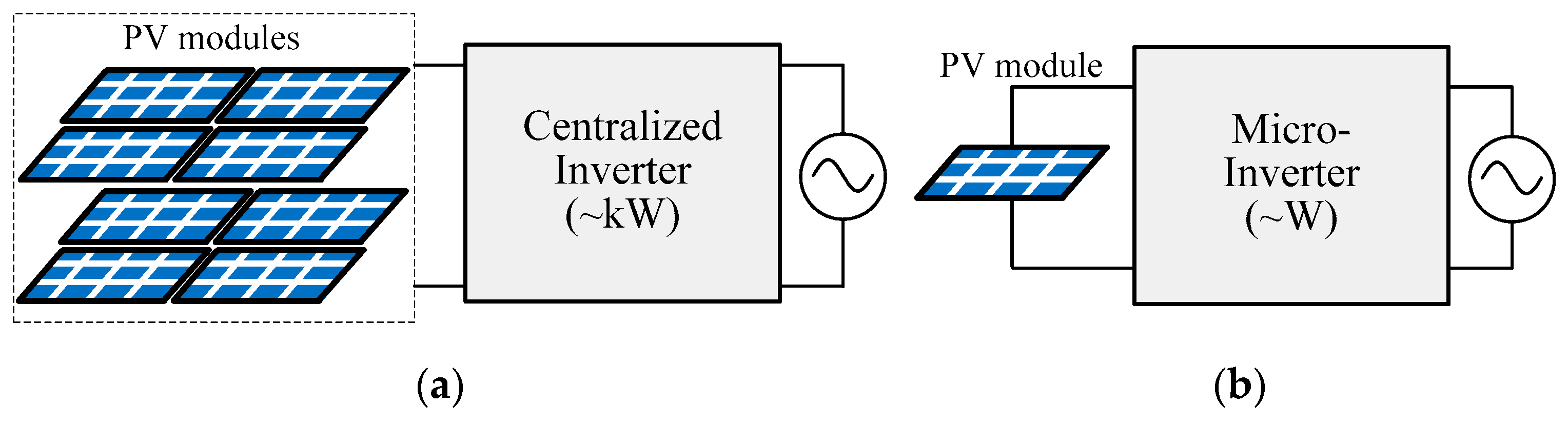
Figure 1 shows the PV power generative system. Typically, the centralized inverter, as shown in Figure 1a, is employed, and the generative DC power is translated to single-phase AC. In this system, each generative power of the PV modules is regulated by the single inverter with a large power rating. On the other hand, the micro-inverter as shown in Figure 1b is integrated to the PV modules, and each power converter is connected to the single-phase grid directly. Therefore, it is possible to optimize the generative power at each of the PV modules.
On the other hand, the micro-inverters require a long lifetime and the PV panels, likewise, are ideally maintenance-free. However, the electrolytic capacitor may decay over the lifetime of the converter. In particular, bulky electrolytic capacitor is necessary on the single-phase AC system in order to compensate the double-line frequency power ripple. In order to solve this problem, the micro-inverter with the active power decoupling circuit is considered in this paper.
Note that the micro-inverter systems are the distributed power supply, and each power converter transfers the generative power to the single-phase AC grid independently. Typically the all-converter operation is regulated by the Power Line Connection (PLC), and it is easy to get some information such as the power generation status. In this system, the micro-inverters are operated independently, and each power converters does not interfere with each other by the circuit operation.
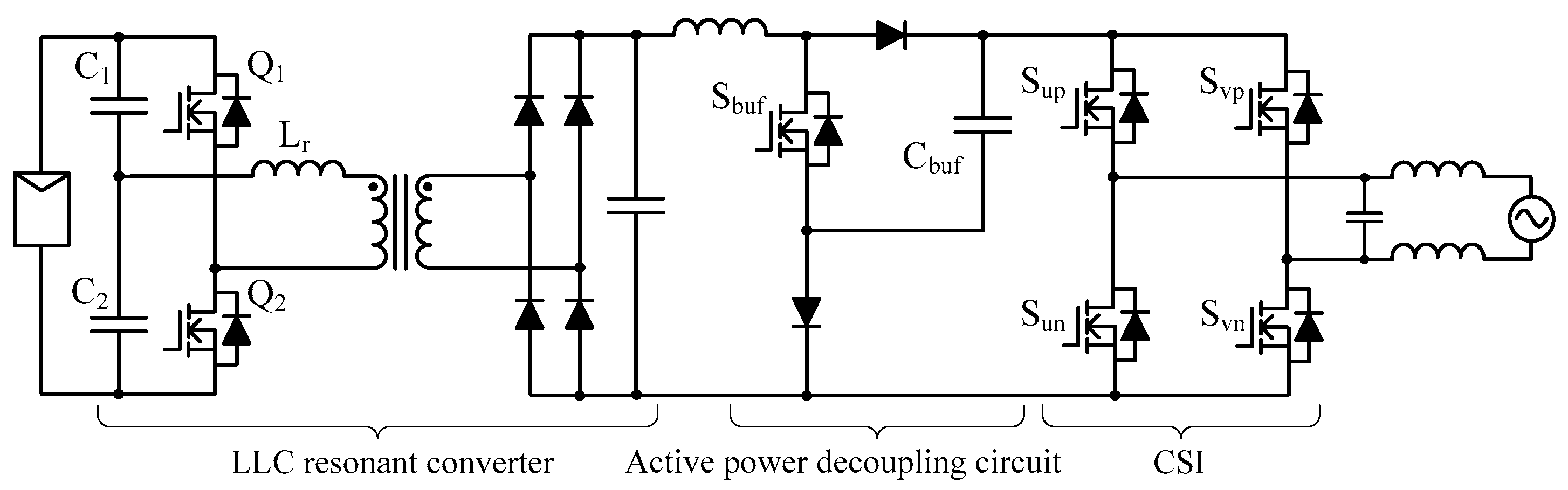
Figure 2 shows the circuit configuration of the DC to single-phase AC converter which consists of LLC resonant converter and an active power decoupling circuit. The active power decoupling circuit compensates the double-line frequency power ripple due to the single-phase grid by the small capacitor [13]. The LLC resonant converter transfers the input power to the secondary side. After that, the boost-up of the DC link voltage and the power decoupling operation are achieved by the active power decoupling circuit. Finally, the grid connection is achieved by the Current Source Inverter (CSI). Note that the reverse-blocking diode is not necessary on CSI because the free-wheeling mode is implemented on the active power decoupling circuit.
3. Operation Principle of Active Power Decoupling Circuit
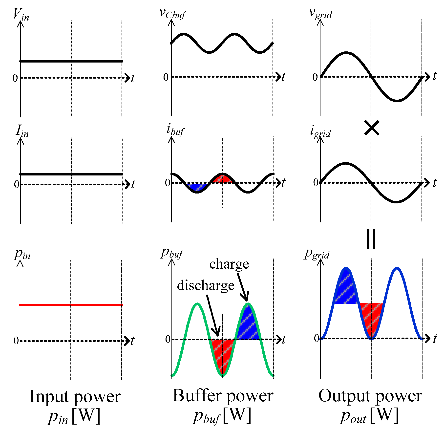
Figure 3 shows the principle of the power decoupling between the DC and single-phase AC sides [14]. In this system, the sinusoidal inverter output current is generated by the power converter in order to transfer the power to the single-phase AC grid. In this case, the single-phase grid voltage and the inverter output current are expressed as
where Vacp is the peak grid voltage and Iacp is the peak inverter current of the single-phase AC grid. When both the output voltage and the current waveforms are sinusoidal, the instantaneous output power pout is expressed as
from (3), the power ripple that contains double-line frequency of the power grid, appears at DC link.
In order to absorb the power ripple, the instantaneous power pbuf should be controlled by
where the polarity of pbuf is defined as positive when the energy Cfc discharges. Due to the power decoupling capability, the input power is matched to the average output power of the single-phase AC. Therefore, the relationship between the input and output power is obtained as
where Vpv is the PV input voltage and Ipv is the PV input current.
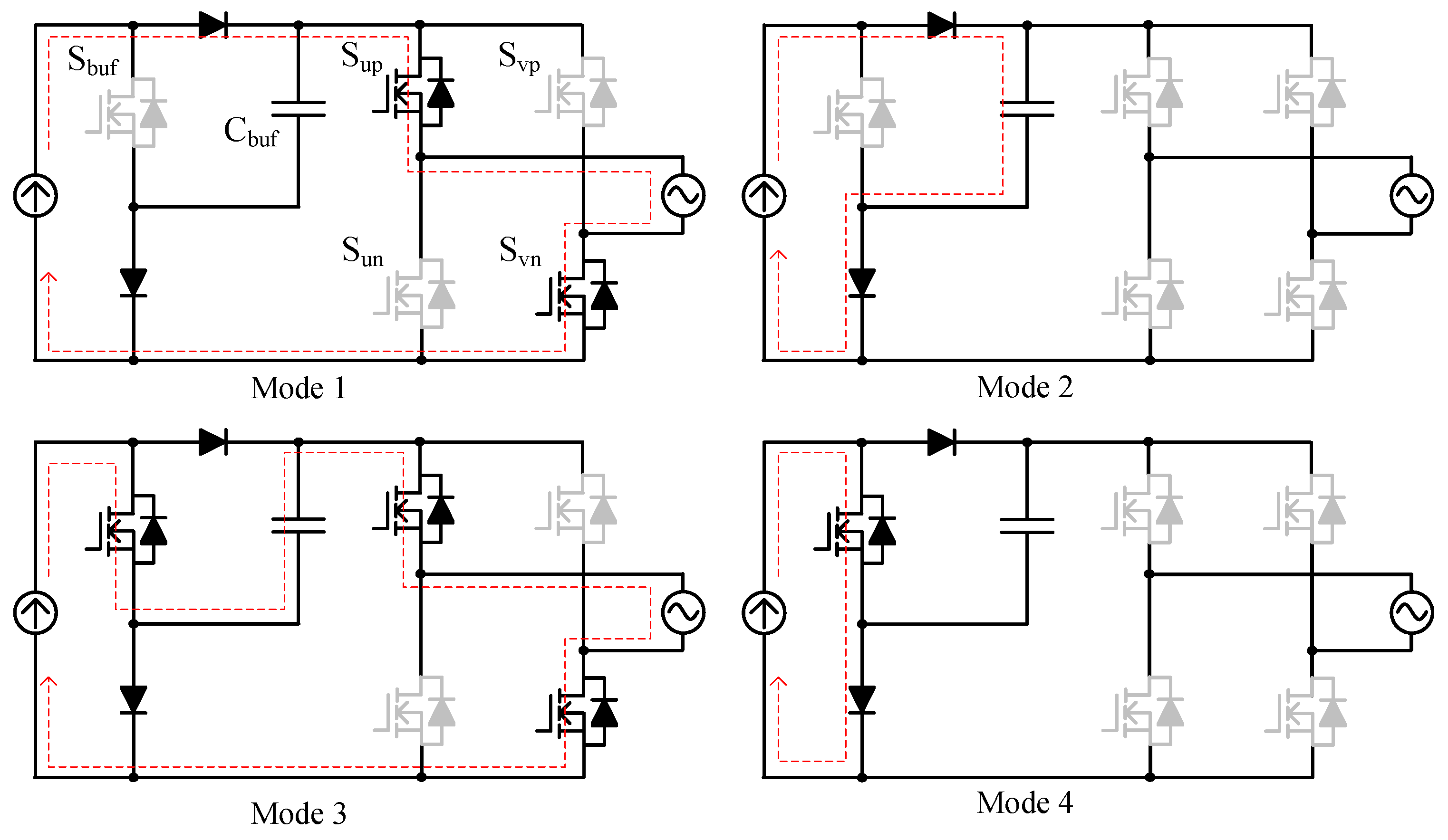
Figure 4 shows the operation mode of the active power decoupling circuit when the grid voltage is the positive period. This converter has the charge mode and discharge mode of the small buffer capacitor Cbuf in order to regulate the capacitor voltage. In order to obtain the buffer power as per Equation (4), the capacitor voltage is actively fluctuated at the twice of the grid frequency such as Figure 3.
The operation of the active power decoupling circuit cooperates with the CSI; this achieves both power decoupling and power transmission to the single-phase AC grid. In mode 1, the switch Sbuf is turned on, and the input power is transferred to the single-phase AC grid. In mode 2, all the switches are turned off, and the buffer capacitor is charged. In mode 3, the buffer capacitor is discharged through the Sbuf and CSI. Finally, mode 4 is the free-wheeling mode. The buffer capacitor voltage is regulated to adjust the duty command for modes 2 and 3 on the one period of the triangle carrier.
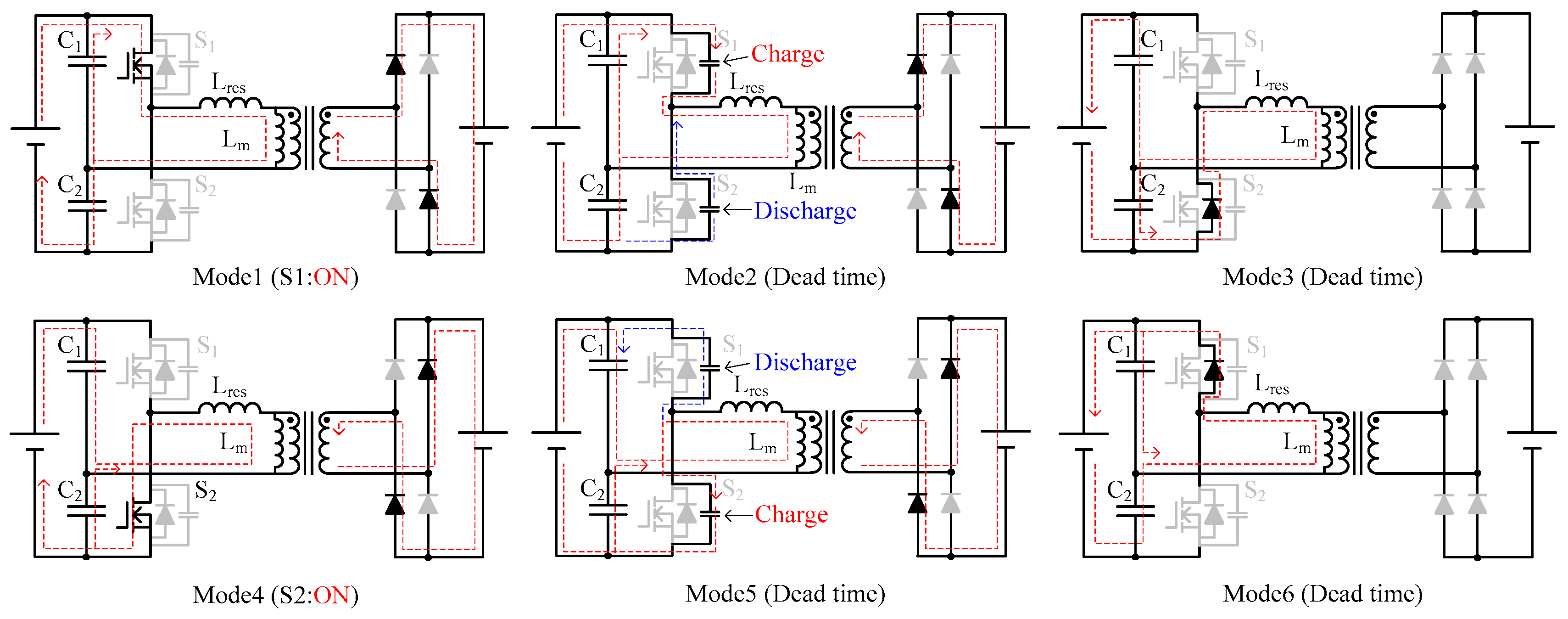
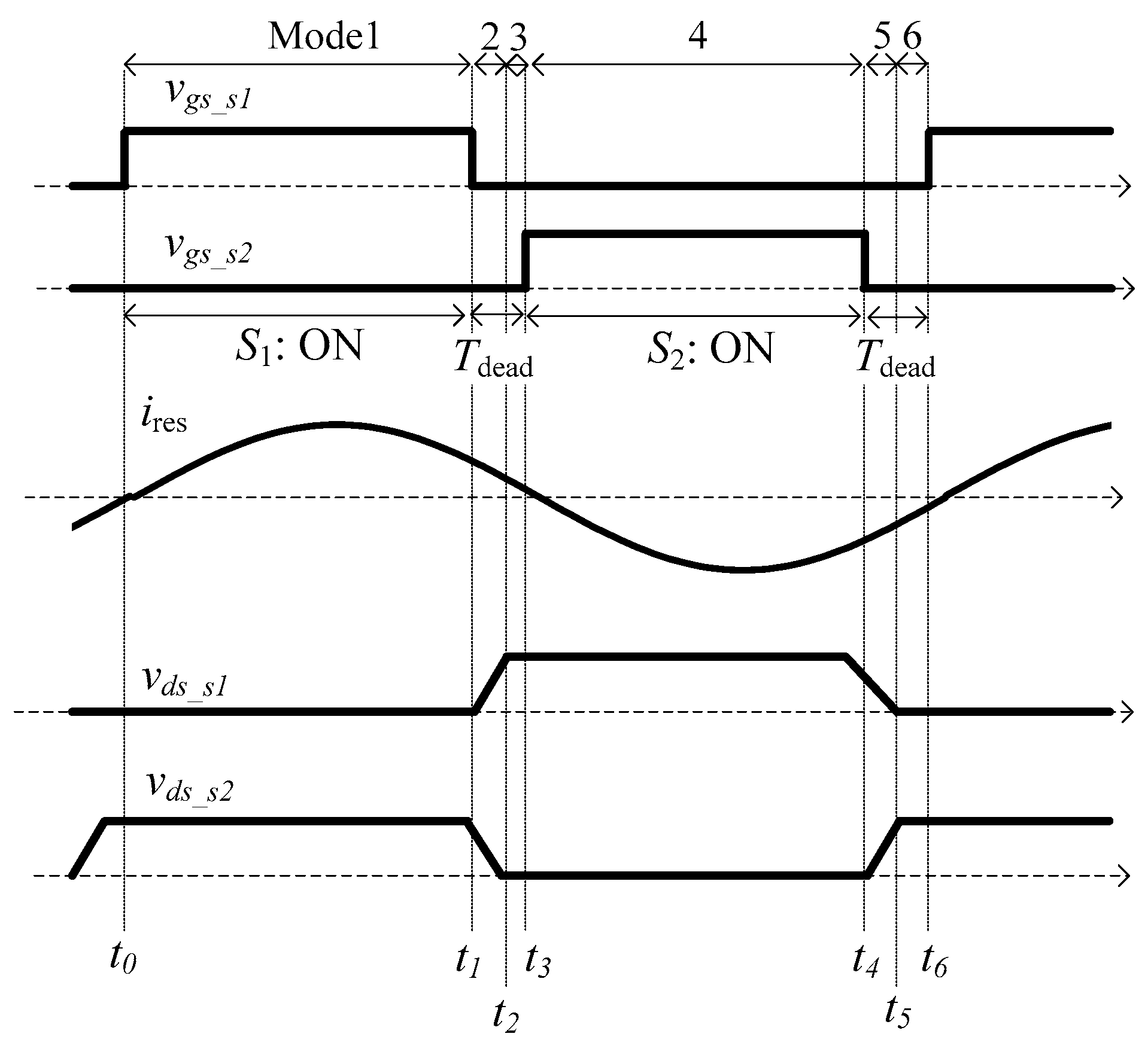
4. Operation Mode of LLC Resonant Converter
Figure 5 shows the operation mode, and the Figure 6 shows the key waveforms of the LLC resonant converter. In this circuit, the series resonance of C1, C2, and Lres is utilized for soft switching. The LLC converter regulates the input voltage of the active power decoupling circuit. The detail of the operation mode is as follows.
Mode 1 [t0-t1]: S1 is turned-on and half of the PV input voltage is applied to the transformer. In this mode, C1, C2, and Lres resonate, and the resonance current occurs.
Mode 2 [t1-t2]: S1 is turned-off and the dead-time period is started. At this mode, S1 achieves ZCS turned off. In mode 2, the parasitic capacitor Cds1 is quickly charged. On the other hand, the parasitic capacitor Cds2 is discharged owing to the negative resonant current. Cds2 is fully discharged in this mode, and mode 3 is started.
Mode 3 [t2-t3]: This mode is still dead-time, and the parasitic diode of S2 conducts. Discharge of Cds2 should be completed during Mode2 and 3 for ZVS of S2.
Mode 4 [t3-t4]: S2 is turned on with ZVS when Cds2 is already discharged. In this mode, C1, C2, and Lres resonate as mode 1, and the resonant current occurs.
Mode 5 [t4-t5]: S2 is turned off, and the dead-time period is started. At this mode, S2 achieves ZCS turned-off. In mode5, the parasitic capacitor Cds1 is quickly charged. On the other hand, the parasitic capacitor Cds1 is discharged owing to the negative resonant current.
Mode 6 [t5-t6]: This mode is still dead-time, and the parasitic diode of S1 conducts. Discharge of Cds1 should be completed during modes 5 and 6 for ZVS of S1.
5. Experimental Result with Fundamental Operation
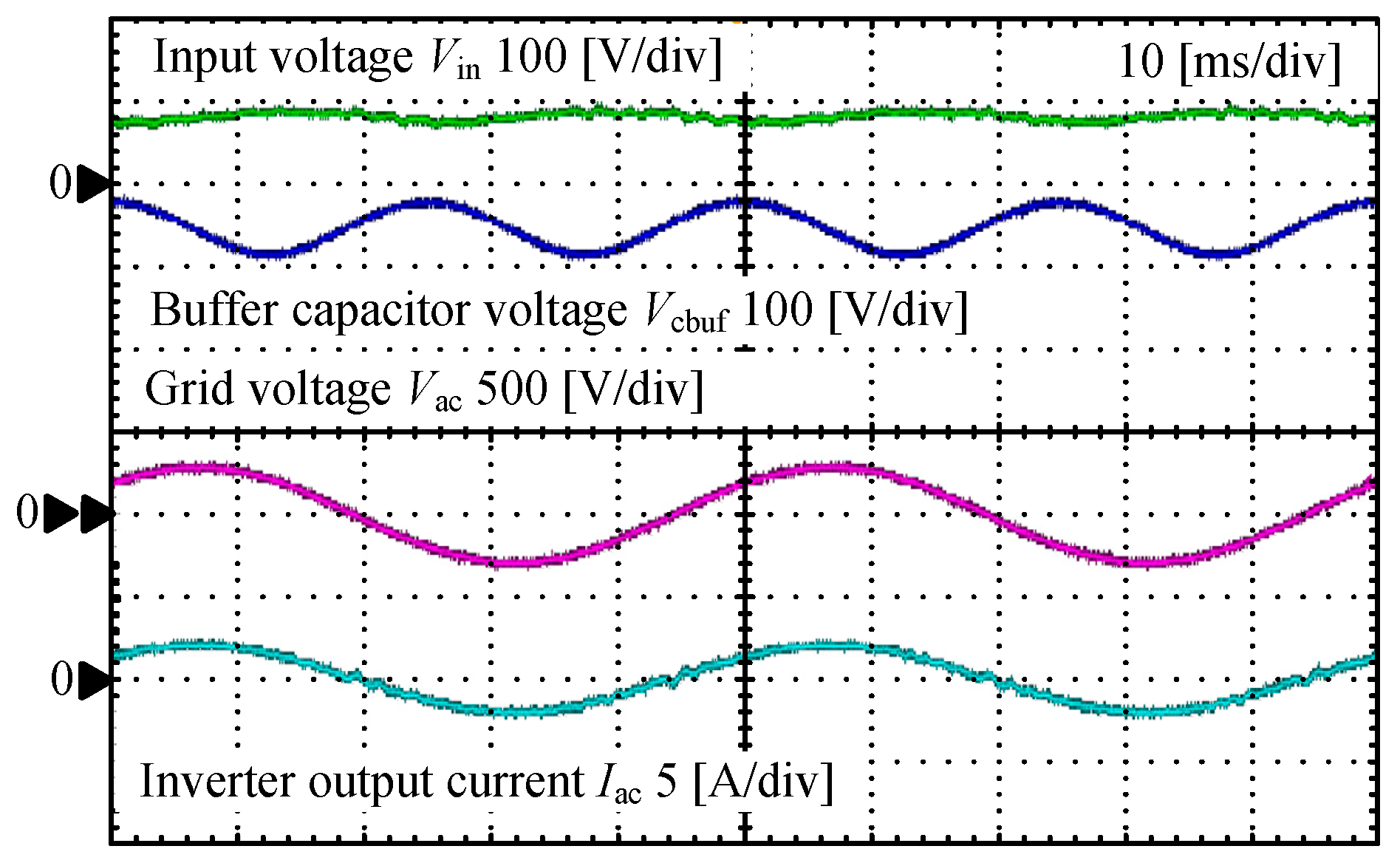
5.1. Active Power Decoupling Circuit and CSI
Table 1 shows the experimental parameters. Figure 7 shows the experimental result. Note that the output power is 300 W, the switching frequency is 20 kHz, the buffer capacitor is 44 µF, and the grid voltage is 200 Vrms.
According to Figure 7, the constant DC voltage and the sinusoidal inverter output current with the low THD are obtained. In addition, it is obtained that the buffer capacitor voltage is fluctuated by the double-line frequency by the power decoupling control. However, the low frequency component is still remaining on the input voltage. This is because the mismatch is occurring during the compensation value and the actual power ripple component. The compensation value for the power decoupling is obtained from the input power. However, the input power is included the conversion loss, which means the error between the compensation power and the actual output power occurs. This problem is solved by changing the calculation process of the compensation value to use the output power condition.
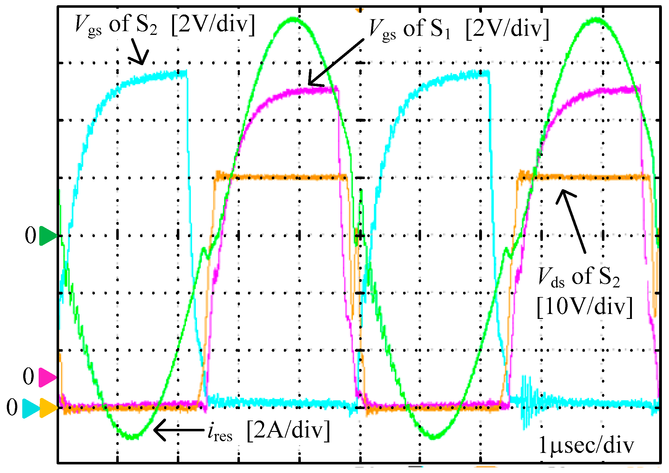
5.2. LLC Resonant Converter
Table 2 shows the experimental parameters and Figure 8 shows the experimental result. Note that the resonant frequency is designed to 205 kHz, and the switching frequency is set to below the resonant frequency as Table 2. In addition, the gate signals of S1 and S2 is provided by the 50% of duty signals from the controller. According to Figure 8, the sinusoidal resonant current is obtained by the series resonance.
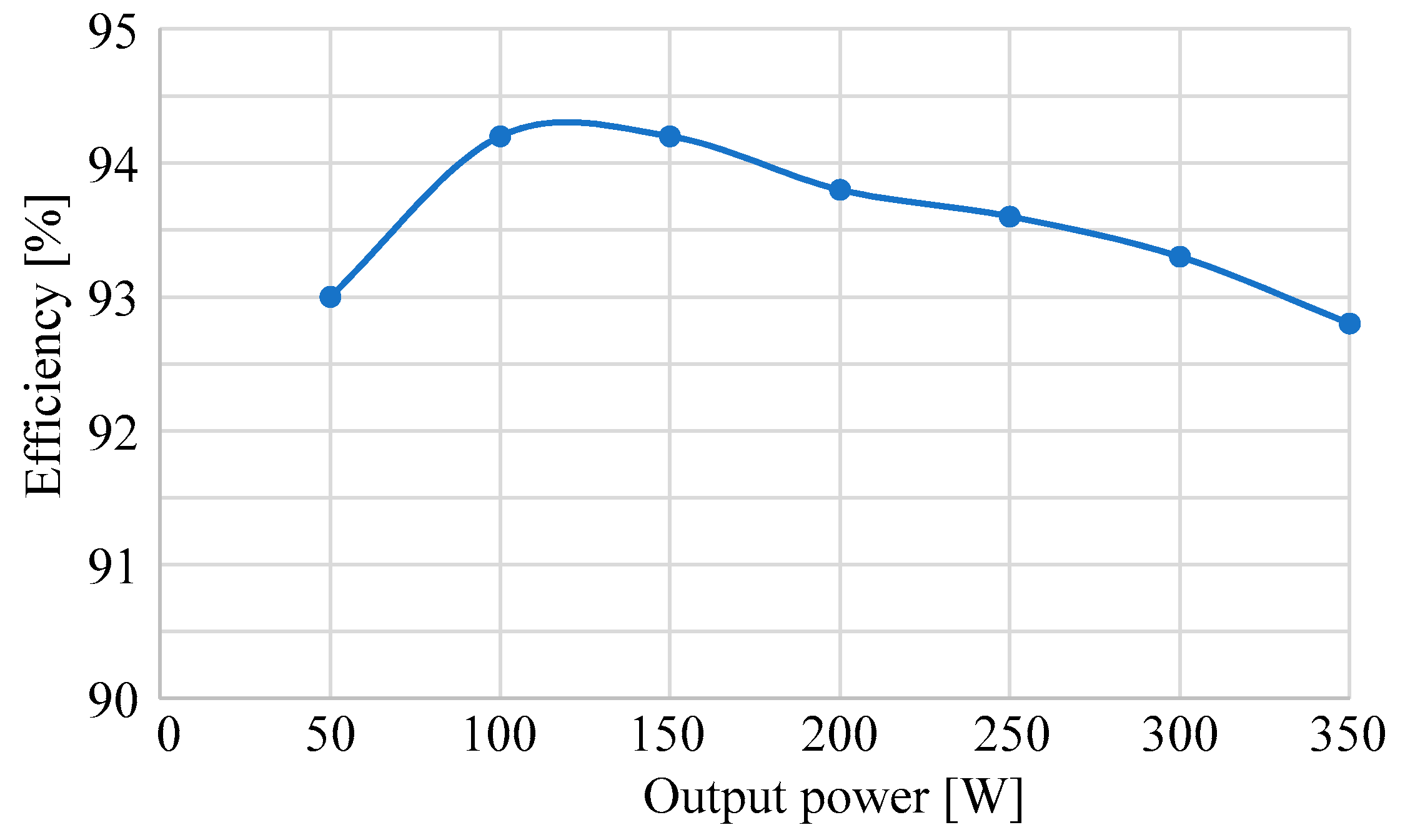
Figure 9 shows the efficiency characteristics and the loss analysis result of the LLC resonant converter. According to Figure 9, 94.3% of the maximum efficiency is obtained when the output power is 100 W. In order to improve the conversion efficiency, the utilization of the synchronous rectifier is simple solution. On the other hand, the reduction of the transformer losses is important for the high switching frequency DC/DC converter because the copper loss becomes largely due to the skin effect and the proximity effect [15].
6. Evaluation of Conversion Efficiency Using Different Litz Wire
In this section, the conversion efficiency of the LLC converter is evaluated in terms of a change the transformer. The high switching frequency operation increases the transformer loss including the copper loss due to the skin effect and the proximity effect, eddy loss, and hysteresis loss. Especially the skin effect and the proximity effect reduce the effective conduction area to surface of the wiring. As the result, the alternative wire resistance becomes large. In order to avoid this problem, the litz wire is usually used. In this paper, the two types of transformer are evaluated when the number of strands is changed.
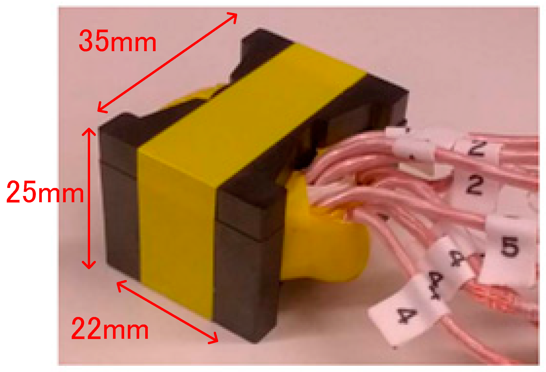
Figure 10 shows the overview of the transformer, and Table 3 and Table 4 show the parameter of the two transformers. Note that the air gap is not provided on this transformer in order to eliminate the leakage flax from the air gap, and the ferrite core with low eddy current loss is selected for the high switching frequency operation. The difference between two transformers is only number of strands, with transformer 2 having many strands on the wiring.
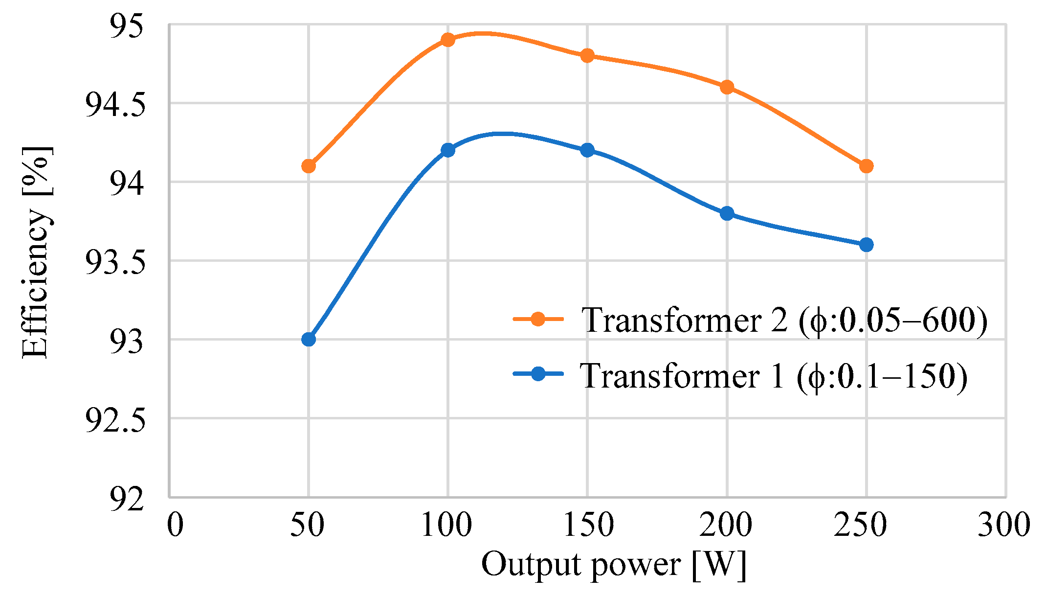
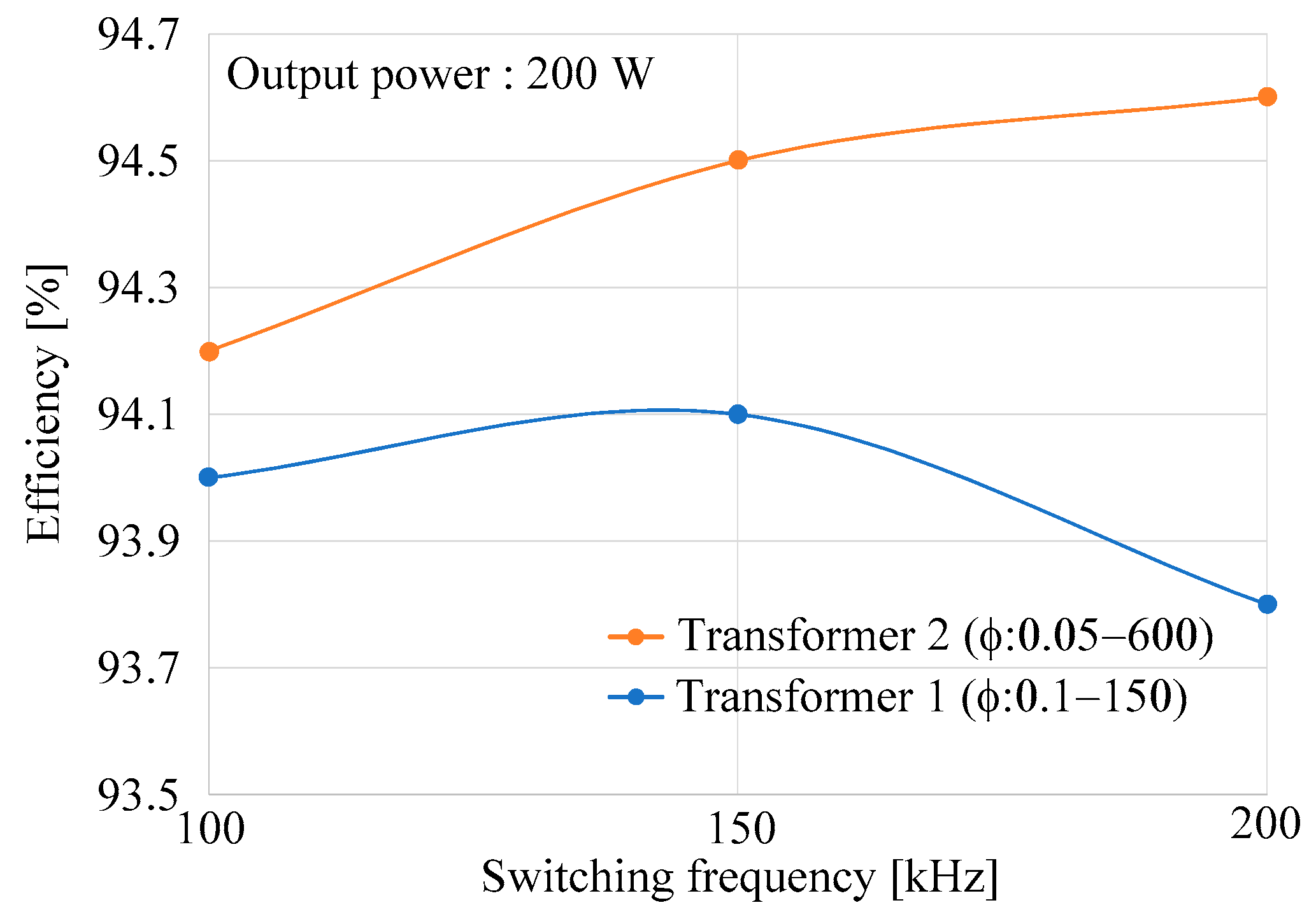
Figure 11 shows the comparison of the conversion efficiency when the number of the strands is changed. Note that the orange and blue line means the approximate curve of each plot. The switching frequency is set to 200 kHz, and the same transformer core material is used. In this experiment, the conversion efficiency of the LLC converter with difference number and diameter of strands as shown in Table 3 is compared. According to Figure 11, it is obtained that the conversion efficiency is improved by 1% when the number of strand is increased on the wiring. This is because the increasing AC resistance due to the skin effect is suppressed, and the copper loss is reduced. Therefore, the litz wire with a lot of strands has a good performance in order to improve the conversion efficiency for the high switching frequency converter. Note that Figure 12 shows the comparison of the conversion efficiency when the switching frequency is changed. Note that the orange and blue lines represent the approximate curve of each plot. According to Figure 12, it is obtained that the improvement rate of the conversion efficiency is increased at 200 kHz. From this result, the number of strands should be chosen accordingly because it depends on the switching frequency.
7. Conclusions
In this paper, a DC–single-phase AC power converter with an LLC resonant converter is presented for a photovoltaic (PV) micro-inverter application. This converter consists of the LLC resonant converter, the active power decoupling circuit, and the CSI. In addition, the conversion efficiency of the LLC converter is evaluated when the number of strands is changed. Through the experimental result, it was obtained that the double-line frequency ripple is compensated by the small capacitor using an active power decoupling circuit. Finally, the conversion efficiency of the LLC converter is improved by 1% when the litz wire have a lot of strands.
In the future work, the optimal design of the high frequency transformer will be considered. In particular, the optimal number of the strand should be considered in order to minimize the transformer loss, and it depends on the switching frequency. Therefore, the relationship between the number of strands and the switching frequency will be analyzed. Finally, the optimal transformer design focusing on the minimum transformer losses will be demonstrated based on the loss analysis.
Author Contributions
Conceptualization, H.W. and J.-i.I.; methodology, H.W.; software, N.K.; validation, N.K., S.N. and J.-i.I.; formal analysis, H.W.; investigation, H.W.; resources, H.W.; data curation, H.W.; writing—original draft preparation, H.W.; writing—review and editing, H.W.; visualization, N.K.; supervision, J.-i.I.; project administration, J.-i.I.; funding acquisition, J.-i.I.
Funding
No external funding.
Acknowledgments
This study was supported by New Energy and Industrial Technology Development Organization (NEDO) of Japan.
Conflicts of Interest
The authors declare no conflicts of interest.
References
- Lee, H.Y.; Yun, J.J. Quasi-Resonant Voltage Doubler with Snubber Capacitor for Boost Half-Bridge DC–DC Converter in Photovoltaic Micro-Inverter. IEEE Trans. Power Electron. 2019, 34, 8377–8388. [Google Scholar] [CrossRef]
- Gautam, A.R.; Fulwani, D. Adaptive SMC for the Second-Order Harmonic Ripple Mitigation: A Solution for the Micro-Inverter Applications. IEEE Trans. Power Electron. 2019, 34, 8254–8264. [Google Scholar] [CrossRef]
- Liao, C.Y.; Lin, W.S.; Chen, Y.M.; Chou, C.Y. A PV Micro-inverter with PV Current Decoupling Strategy. IEEE Trans. Power Electron. 2019, 32, 6544–6557. [Google Scholar] [CrossRef]
- Leuenberger, D.; Biela, J. PV-Module-Integrated AC Inverters (AC Modules) with Subpanel MPP Tracking. IEEE Trans. Power Electron. 2017, 32, 6105–6118. [Google Scholar] [CrossRef]
- Sun, W.; Xing, Y.; Wu, H.; Ding, J. Modified High-Efficiency LLC Converters with Two Split Resonant Branches for Wide Input-Voltage Range Applications. IEEE Trans. Power Electron. 2018, 33, 7867–7879. [Google Scholar] [CrossRef]
- Qian, T.; Qian, C. An Adaptive Frequency Optimization Scheme for LLC Converter with Adjustable Energy Transferring Time. IEEE Trans. Power Electron. 2019, 34, 2018–2024. [Google Scholar] [CrossRef]
- Yamamoto, T.; Konno, Y.; Sugimura, K.; Sato, T.; Bu, Y.; Mizuno, T. Loss Reduction of LLC Resonant Converter using Magnetocoated Wire. IEEJ J. Ind. Appl. 2019, 8, 51–56. [Google Scholar] [CrossRef]
- Yamamoto, T.; Bu, Y.; Mizuno, T.; Yamaguchi, Y.; Kano, T. Loss Reduction of Transformer for LLC Resonant Converter Using a Magnetoplated Wire. IEEJ J. Ind. Appl. 2018, 7, 43–48. [Google Scholar] [CrossRef]
- Kimura, S.; Nanamori, K.; Kawakami, T.; Imaoka, J.; Yamamoto, M. Allowable Power Analysis and Comparison of High Power Density DC-DC Converters with Integrated Magnetic Components. IEEJ J. Ind. Appl. 2017, 6, 463–472. [Google Scholar] [CrossRef]
- Liu, B.; Liu, Z.; Liu, J.; Wu, T.; Wang, S. A feedforward control based power decoupling scheme for voltage-controlled grid-tied inverters. In Proceedings of the IEEE Applied Power Electronics Conference and Exposition, Long Beach, CA, USA, 20–24 March 2016; pp. 3328–3332. [Google Scholar]
- Liu, X.; Dong, D.; Harfman-Todorovic, M.; Garaces, L. A PV Micro-inverter With PV Current Decoupling Strategy. In Proceedings of the IEEE Applied Power Electronics Conference and Exposition, Long Beach, CA, USA, 20–24 March 2016; pp. 3403–3408. [Google Scholar]
- Roßkopf, A.; Bär, E.; Joffe, C. Influence of Inner Skin-and Proximity Effects on Conduction in Litz Wires. IEEE Trans. Power Electron. 2014, 29, 5454–5461. [Google Scholar] [CrossRef]
- Ohnuma, Y.; Orikawa, K.; Itoh, J.I. A Single-Phase Current Source PV Inverter with Power Decoupling Capability Using an Active Buffer. In Proceedings of the IEEE Energy Conversion Congress and Exposition, Denver, CO, USA, 15–19 September 2013; pp. 3094–3101. [Google Scholar]
- Watanabe, H.; Itoh, J.I. Zero Voltage Switching Scheme for Flyback Converter to Ensure Compatibility with Active Power Decoupling Capability. In Proceedings of the International Power Electronics Conference, Niigata, Japan, 20–24 May 2018; pp. 896–903. [Google Scholar]
- Hurley, W.G.; Wolfle, W.H.; Breslin, J.G. Optimized Transformer Design: Inclusive of High-Frequency Effects. IEEE Trans. Power Electron. 1998, 13, 651–659. [Google Scholar] [CrossRef]
Figure 1.
Configuration of PV power generative system. (a) Centralized inverter and (b) micro-inverter.
Figure 1.
Configuration of PV power generative system. (a) Centralized inverter and (b) micro-inverter.

Figure 2.
Circuit configuration of DC to Single-phase AC converter using LLC resonant converter.

Figure 3.
Principle of power decoupling between DC and single-phase AC.

Figure 4.
Operation mode of active power decoupling circuit.

Figure 5.
Operation mode of LLC resonant converter.

Figure 6.
Key waveforms of LLC resonant converter.

Figure 7.
Experimental result of active power decoupling circuit and current source inverter (CSI).

Figure 8.
Switching waveforms.

Figure 9.
Efficiency curve.

Figure 10.
Overview of high frequency transformer.

Figure 11.
Comparison of conversion efficiency when number of strands is changed on wiring.

Figure 12.
Comparison of conversion efficiency when switching frequency is changed.


Table 1.
Experimental parameters.
| Symbol | Quantity | Value |
|---|---|---|
| Vin | Input Voltage | 90 V |
| Pin | Input Power | 300 W |
| Cbuf | Buffer Capacitor | 44 µF |
| Vac | Grid Voltage | 200 Vrms |
| fac | Grid frequency | 50 Hz |
| fsw | Switching frequency | 20 kHz |
Table 2.
Experimental parameters.
| Symbol | Quantity | Value |
|---|---|---|
| Vin | Input Voltage | 40 V |
| Vout | Output Voltage | 80 V |
| fsw | Switching frequency | 200 kHz |
| Lm | Magnetizing inductance | 25 µH |
| Lres | Resonant inductance | 400 nH |
| C1, C2 | Resonant capacitance | 750 nF |
| Cdc | DC capacitance | 15 µF |
| Cj | Junction capacitance | 500 pF |
| Coss | Output capacitance | 1500 pF |
Table 3.
Parameters of transformer 1.
| Symbol | Quantity | Value |
|---|---|---|
| N1 | Primary side number of turns | 2 |
| N2 | Secondary side number of turns | 8 |
| - | Litz wire specification | 150/ϕ0.1 |
| - | Current density | 4 A/mm2 |
| - | Core material | Ferrite (PQ) |
| - | Air gap | 0 mm |
| Lm | Magnetizing inductance | 21.3 µH |
Table 4.
Parameters of transformer 2.
| Symbol | Quantity | Value |
|---|---|---|
| N1 | Primary side number of turns | 2 |
| N2 | Secondary side number of turns | 8 |
| - | Litz wire specification | 600/ϕ0.05 |
| - | Current density | 4 A/mm2 |
| - | Core material | Ferrite (PQ) |
| - | Air gap | 0 mm |
| Lm | Magnetizing inductance | 21.5 µH |
© 2019 by the authors. Licensee MDPI, Basel, Switzerland. This article is an open access article distributed under the terms and conditions of the Creative Commons Attribution (CC BY) license (http://creativecommons.org/licenses/by/4.0/).
Share and Cite
MDPI and ACS Style
Watanabe, H.; Itoh, J.-i.; Koike, N.; Nagai, S. PV Micro-Inverter Topology Using LLC Resonant Converter. Energies 2019, 12, 3106. https://doi.org/10.3390/en12163106
AMA Style
Watanabe H, Itoh J-i, Koike N, Nagai S. PV Micro-Inverter Topology Using LLC Resonant Converter. Energies. 2019; 12(16):3106. https://doi.org/10.3390/en12163106
Chicago/Turabian StyleWatanabe, Hiroki, Jun-ichi Itoh, Naoki Koike, and Shinichiro Nagai. 2019. "PV Micro-Inverter Topology Using LLC Resonant Converter" Energies 12, no. 16: 3106. https://doi.org/10.3390/en12163106
Note that from the first issue of 2016, this journal uses article numbers instead of page numbers. See further details here.