6.78-MHz, 50-W Wireless Power Supply Over a 60-cm Distance Using a GaN-Based Full-Bridge Inverter


1
School of Electrical and Computer Engineering, University of Seoul, Seoul 02504, Korea
2
Smart Electrical & Signaling Division, Korea Railroad Research Institute, Uiwang 16105, Korea
*
Author to whom correspondence should be addressed.
Energies 2019, 12(3), 371; https://doi.org/10.3390/en12030371
Submission received: 3 January 2019
/
Revised: 18 January 2019
/
Accepted: 21 January 2019
/
Published: 24 January 2019
(This article belongs to the Special Issue Design and Control of Power Converters 2019)
Abstract
:An inductive wireless power transfer system is proposed as a power supply for an on-line monitoring system for an overhead catenary. Because of the high voltage (25 kVrms) applied to the catenary, galvanic isolation was required to supply power to the attached monitoring system. The proposed wireless power system was able to transmit 50 W over a distance of 60 cm at 6.78 MHz. Design methodologies for the transmitter and the receiver coils, 6.78-MHz GaN-based full-bridge inverter, and rectifier are proposed in this paper. Pareto optimality, a multi-objective optimization technique, was used to determine optimal solutions in terms of efficiency and copper usage. A 100-W, 6.78-MHz full-bridge inverter was developed using 100 V, 35 A, E-HEMT GaN MOSFETs. Because of the high operating frequency, two factors were considered in the design of the full-bridge inverter, (1) close placement of the gate driver and the switch to minimize parasitic inductance and the resulting fluctuation of the drive signal and (2) effective heat dissipation from the switches and gate drivers for a high power rating. In addition, a full-wave rectifier was built using Schottky barrier diodes with a reverse recovery time of a few tens of nano-seconds. The developed wireless power system was experimentally evaluated. The measured coil-to-coil efficiency was 77%, and the measured efficiencies of the inverter and the rectifier were 92% and 93%, respectively. The overall system efficiency was 57% for a transfer of 47 W. Finally, the dependences of the efficiency on the distance, operating frequency, and load were evaluated.
1. Introduction
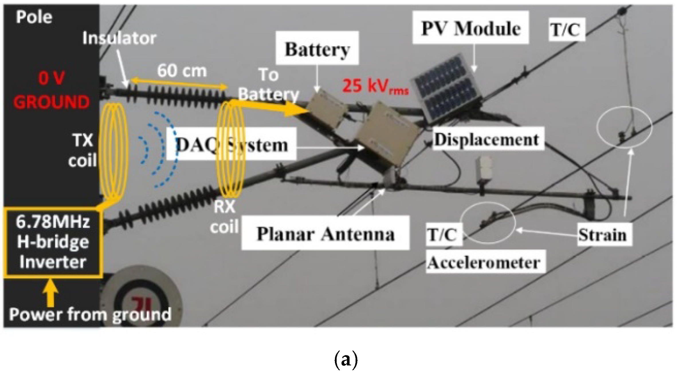
Applications of inductive wireless power transfer (WPT) technology have transitioned from W level biomedical devices to MW level transportation systems [1,2,3,4,5,6,7,8]. Among the various applications, application that the WPT system is useful as a power supply: an on-line monitoring system for a high-voltage catenary (see Figure 1a) [9]. Because of the high-voltage (25 kVrms) of the catenary, the monitoring system cannot obtain power from a low-voltage grid (110 Vrms or 220 Vrms) without having a sufficient insulation or isolation gap. According to [10], the minimum isolation distance between a 25-kVrms overhead wire and ground is 25 cm (30-cm isolation distance is recommended). This is the reason that the lengths of the insulators used for 25-kVrms catenaries are longer than 30 cm (60 cm or longer insulators are common). Therefore, any system that supplies a low voltage power to the 25-kVrms catenary needs to transmit power over the lengths of the insulators.
Previously, a 12-V, 12-Ah Pb-battery and a photovoltaic (PV) battery charger were used as an energy source. The PV charger was attached to an arm of a support pole (see Figure 1a). It solved the high voltage isolation problem. However, the size and weight of the PV module required to supply sufficient power (larger than 50 W) to the monitoring system were too large and heavy to be installed on the arm.
Instead of the PV module, an inductive WPT system was proposed that is able to wirelessly transmit energy over the insulator in [11,12]. According to [13], the inductive WPT system was more efficient compared to other technologies like a capacitive WPT system or a far-field power radiating system. The distance between the coils of the target WPT system was over 60 cm and output power was 50 W. The operating frequency of the system was 6.78 MHz (the highest frequency allowed for a WPT system [14]) to achieve efficient power transmission for this large air-gap. Because of the high operating frequency and large output power, the development of low-loss transmitter and receiver coils and a high efficiency 6.78-MHz inverter are required to construct an effective WPT system. There have been many previous studies that worked on such large air-gap, MHz frequencies WPT systems.
Sample et al. proposed a 7.65-MHz, 70-cm distance WPT system in 2011 [15]. The authors used two circular coils with diameters of 59 cm as a transmitter and a receiver. The measured coil-to-coil efficiency was 70% at 30 W, 70-cm power transmission. The main focus of the paper was to determine the optimal operating frequencies depending on the change of the distance between the coils. Duong and Lee published a paper demonstrating 30-mW transmission over a distance of 60 cm with a peak efficiency of 46% [16]. In this paper, the main focus of the paper was a mathematical analysis of the coil-to-coil system using an equivalent circuit modeling technique. Lee et al. proposed a coil design methodology for a large air-gap system in [17]. The design methodology identified a feasible design space as its first step. Then the coil-to-coil efficiency, copper usage, control stability, and other performance metrics were calculated in the entire design space, and a weighted sum of the metrics was calculated to determine an optimal design for the transmitter and the receiver coils. Based on the proposed methodology, a 95% coil-to-coil efficiency was achieved at a distance of 30 cm and 3.74-MHz operation. However, these aforementioned papers did not consider the feasibility and efficiency of MHz operation inverters, even though it is challenging to build an efficient high-power converter at these high frequencies.
The literature [18,19,20,21,22] focused on the development of high efficiency MHz switching class-E amplifiers for loosely-coupled WPT systems. Class-E amplifiers are very common in radio-frequency (RF) application since the amplifier requires only one low-side switch for power conversion. However, the class-E inverter requires a bulky DC inductor, and the optimal circuit parameters (e.g., shunt capacitances) are highly dependent on the operating conditions (load, duty cycle, and operating frequency, etc.) [23]. Therefore, the class-E inverter requires fine tuning of the circuit parameters depending on the load and operation conditions.
Instead of the class-E inverter, recent rapid evolution of large bandgap semiconductor switches (Silicon-carbide (SiC) and Gallium-nitride (GaN) Metal-Oxide-Semiconductor Field-Effect Transistor (MOSFET)) and their gate drivers have enabled significant advancement of radio-frequency half- and full-bridge switch-mode inverters. Multiple papers reported on GaN-based full-bridge inverters for WPT systems in 2017 [24,25,26]. Zhao et al. proposed a multi-frequency pulse-width-modulation (MFPWM) scheme which was implemented using a GaN-based full-bridge inverter [24]. Using MFPWM, an inverter can simultaneously transmit power to two receivers that operate at 100 kHz and at 6.78 MHz. Since the focus of the research was the transmission of power to multiple receivers, rather than improvement of the inverter efficiency using GaN switches, the efficiency of the developed inverter was not sufficiently high to be used for a system operating at a few tens of Watts. Bonache-Samaniego et al. proposed a self-oscillating resonant converter that operates at 6.78 MHz [25]. The gate signals of the developed full-bridge inverter’s GaN switches were generated using the sensed current of the resonant tank. The proposed system was useful in the construction of a low cost and simple inverter. However, it was not suitable for the control of the operating frequency, duty, or power level. Xue and Zhang demonstrated a 50-W, 6.78-MHz, 90% efficiency GaN-based inverter for a WPT system. The main focus of the paper was the design of a filter network to achieve a wider zero-voltage-switching (ZVS) range and higher efficiency at light loads. The research used a 13.56-MHz oscillator and a D-flip-flop to generate a 6.78-MHz gate drive signal. The output power was controlled using a phase-shift control of the legs of the inverter based on a phase delay element.
In this paper, a novel 50-W, 60-cm distance wireless power system operating at a frequency of 6.78 MHz is proposed. The design and fabrication methodologies for the transmitter and the receiver coils, a 100-W, 6.78-MHz H-bridge inverter using GaN switches, and a 50-W, 6.78-MHz full-wave rectifier design are investigated. The power level and efficiency of the proposed system were experimentally evaluated. In the first part of the paper, design methodology for the transmitter and receiver coil is proposed using a Pareto optimality, a multi-objective optimization technique. The designed coils are fabricated on a printed-circuit-board (PCB) for ease of mass-production. The dominant sources of losses of the PCB coils are identified and the methods for fabrication of low-loss coils at 6.78-MHz frequencies are presented. The details of a 100-W, 6.78-MHz operating E-HEMT GaN-based H-bridge inverter is explained in the following section. The H-bridge inverter is developed to supply power to the transmitter coil. The gate signals of the switches are controlled using a commercial 32-bit digital-signal-processor, and the details of the PCB layout techniques for low parasitic inductance and an effective heat dissipation are discussed. Finally, the performance evaluation of the developed system is presented using experimental results. Efficiencies and losses of each component of the system are measured and compared. Also, the dependence of the DC-to-DC efficiency on the distance, load, and operating frequency is evaluated with the test-bed.
2. Target System Configuration
A photo of the target catenary monitoring system is shown in Figure 1a. The catenary monitoring system has multiple sensors that were installed on the catenary, a data acquisition (DAQ) system that gathers information from the sensors and wirelessly transmits the information to a data center, and a battery pack as an energy source. A WPT system that can transmit 50 W over a 60-cm distance (the length of the insulator) is proposed. A schematic of the proposed WPT system is shown in Figure 1b. The proposed WPT system collects power from a 220-Vrms single-phase grid and converts it to DC with a diode rectifier. Then, it is converted to a 6.78-MHz AC voltage and supplied to the transmitter (TX) coil using a GaN-based H-bridge inverter. The induced voltage of a receiver coil that is weakly coupled to the transmitter is rectified and supplied to the battery using a full-wave diode rectifier. The design details of the transmitter and the receiver coils, 6.78-MHz resonant inverter, and receiver side rectifier are described in following sections.
3. Development of Transmitter and Receiver coils
3.1. Transmitter and Receiver coil Design
There were three main constraints with regard to the design of the transmitter (TX) and the receiver (RX) coils; (1) the maximum sizes of the TX and RX coils were limited to 40 cm × 40 cm, (2) the minimum distance between the TX and RX coil was 60 cm. (3) the required output power was 50 W, and load resistance was 6 Ω. For full utilization of the given space, square coils were assumed for the TX and RX coils as shown in Figure 2. The design parameters to be determined for a square coil were the inner diameter (), turn spacing (s), width of the turn (w), and the number of turns of the transmitter and the receiver coils (ntx and nrx). The design spans for the parameters are summarized in Table 1.
Pareto optimality [27], a multi-objective optimization theory, was applied in the coil design process. The maximization of the power transfer efficiency () and minimization of the total usage of the copper () were two objectives during optimization. The power transfer efficiency and total mass of the copper depending on the coil shape change were calculated using (1) [28] and (2).
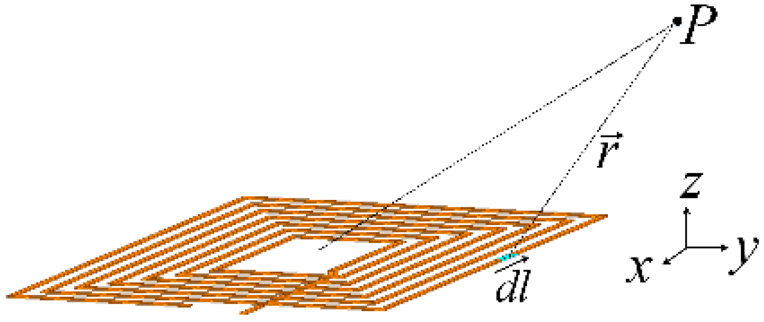
where, is the operating frequency of the system, M is the mutual inductance between the transmitter and the receiver, and are the equivalent series resistances (ESRs) of the transmitter and the receiver coils, respectively, is the load resistance of the system, is the density of the copper, and t are the total length, width, and the thickness of the coil trace, respectively. The mutual inductance and the ESRs of the TX and RX coils were calculated for each combination of the inner diameter, turn-spacing, width of the turn, and the number of the turns. The mutual inductance was calculated using a numerical integration of the flux linkage between the coils. According to [29], the z-directional magnetic field intensity at point P () generated by a square transmitter coil follows (3).
Then, the total flux linkage () at the receiver coil and resulting mutual inductance (M) can be calculated. Hz is the z-directional magnetic field intensity at point P, I is the current flowing in the transmitter coil, ntx is the number of turns of the transmitter coil, is the infinitesimal displacement vector of i-th turn of the transmitter and is a direction vector from to the point (see Figure 3), is the infinitesimal area element in k-th turn of the receiver coil, is the permeability of air, is the total flux linkage at receiver coil, and M is the resulting mutual inductance. The ESRs of the transmitter and the receiver coils were calculated using (4).
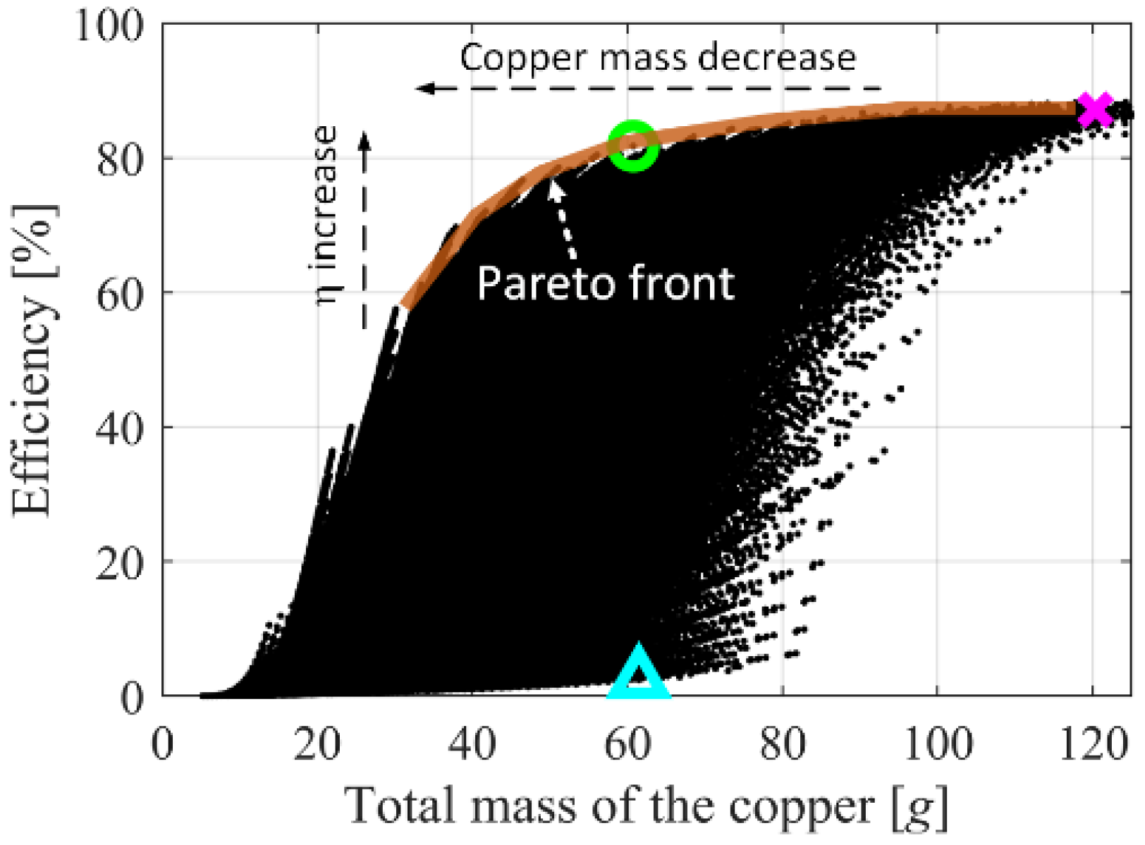
where is the total length of the coil, w is the width of the trace of the coil, is the conductivity of copper, and (= 25.4 μm) is the skin-depth of the copper at 6.78 MHz. Figure 4 shows a distribution in the entire coil design space.
From the figure, it should be noted that the WPT coils with the same total mass of copper have very different efficiencies depending on their design. For example, the first WPT system (identified by the cyan triangular point in Figure 4 had an 8-turn transmitter coil with a 10 cm inner diameter, 40 cm outer diameter, 6 mm of turn spacing, and 13 mm turn width. The receiver of the first WPT system was a 1-turn coil with a 10 cm inner diameter, 12.6 cm outer diameter, 6 mm of turn spacing, and 13 mm turn width. The second WPT system (identified by green circular point in Figure 4 had a 3-turn transmitter coil with a 30 cm inner diameter, 40 cm outer diameter, 5 mm of turn spacing and 13 mm turn width. Its receiver coil was a 3-turn with a 30 cm inner diameter, 40 cm outer diameter, 5 mm of turn spacing, and 13 mm turn width. The total mass of both systems was 60 g; however, the power transfer efficiency of the first system was 2.4% at 60 cm of air-gap while the efficiency of the second system was 82%.
Since the goal function was to maximize the efficiency while minimizing copper usage, non-dominated solutions (Pareto front) were located at the upper left corner of the plot. The brown line in the figure represents the Pareto front. Among the non-dominated solutions, one of the solutions with 87% efficiency and 110 g of copper usage was selected for the TX and RX coil design. This solution is denoted as a magenta X in the plot. It is notable that the decision was made for high efficiency rather than low copper mass. The selected design parameters for the TX and RX coils are summarized in Table 2.
3.2. Finite Element Analysis of Transmitter and Receiver
The selected design was evaluated by finite element analysis (FEA) results using the full-wave simulation software ANSYS HFSS (19.0, ANSYS, Canonsburg, PA, USA) and ANSYS DESIGNER (19.0, ANSYS, Canonsburg, PA, USA). Figure 5a shows a simulation model of the WPT system and Figure 5b shows the resulting coil-to-coil efficiency vs. operating frequency for a 6 Ω load. The theoretical efficiency was calculated using (1). It should be noted that the theoretical and the simulated results are in good agreement with each other.
3.3. High Q coil Fabrication
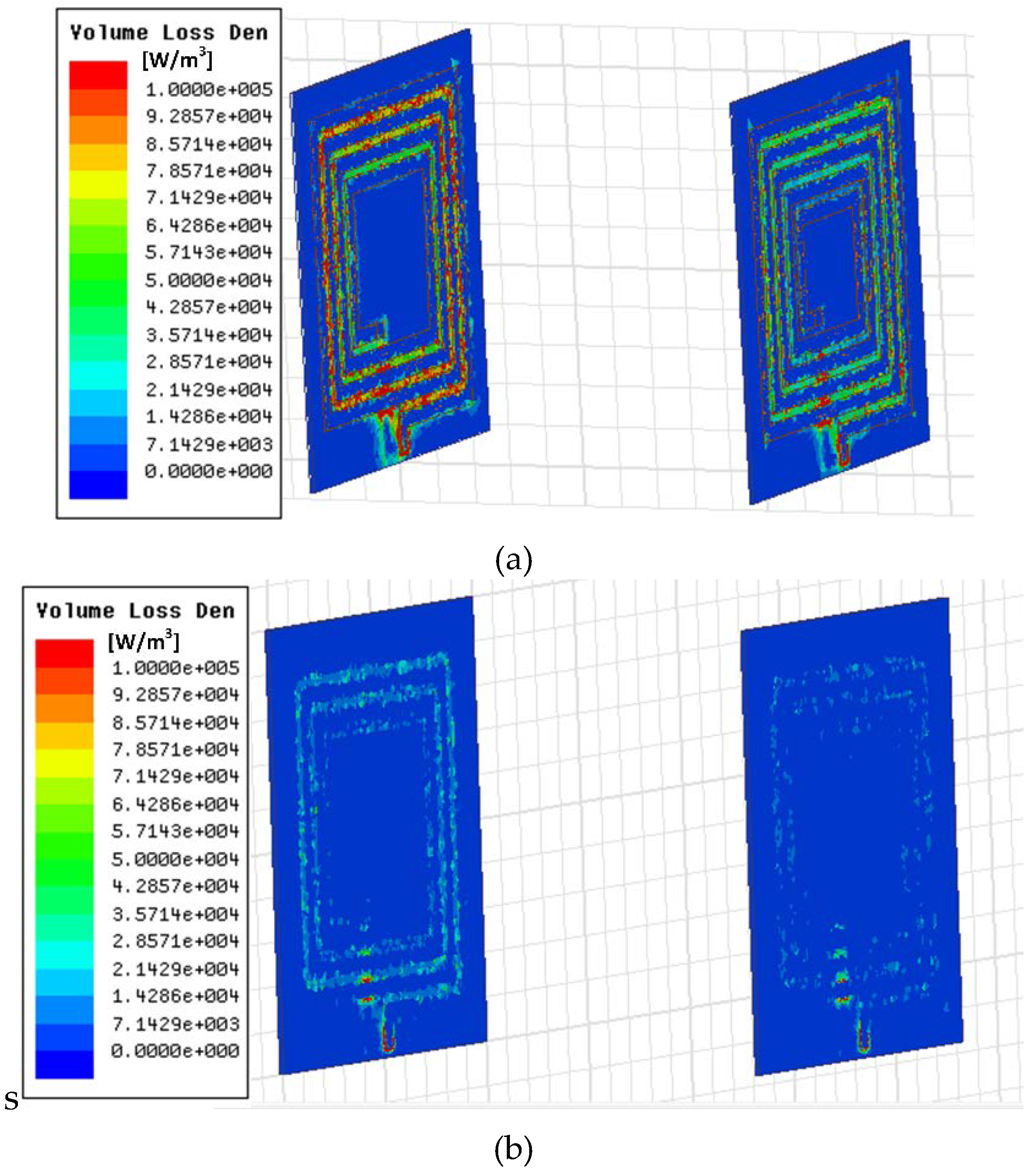
Because of the large diameter and a small number of turns of the TX and RX coils, the coils were fabricated using a PCB for ease of mass-production. Fabrication of a high-quality factor transmitter and the receiver coils on the PCB is discussed in a previous paper [12]. A summary of the previous paper is provided in this chapter. At high frequencies, especially in the MHz frequency ranges, the reduction of three primary types of losses was important to achieve high quality factor (Q-factor) coils on the PCB. These include skin-effect loss, proximity-effect loss, and dielectric loss. Because of the target WPT system’s high operating frequency, skin- and proximity-effect losses were critical in the process of analyzing the Ohmic loss of the copper trace. In addition, the dielectric loss of the PCB substrate was important in determining the entire loss of the PCB coil because it can dominate other losses when the coil is not designed properly. According to the full-wave simulation results in [12], the dielectric loss was approximately 10 times greater than the Ohmic loss when the PCB substrate was a very common material, FR-4. A low dissipation factor PCB material (IS680 [30]) was very effective in reducing dielectric loss (see Table 3). Figure 6a,b show the distributions of the dielectric losses at the transmitter and the receiver coils when they transfer 50 W to a load.
It should be noted that the transmitter and receiver coils using FR-4 substrates have much higher dielectric losses compared to the losses associated with the coils using the IS680 substrates. For further reduction of the dielectric loss, compensation capacitors were distributed in the middle of the coil windings as shown in Figure 7. This was helpful in reducing the electric field intensities between the adjacent turns and additional improvements of the Q-factors of the coils [12]. Figure 7 shows photos of the printed transmitter and receiver coils on IS680 substrates with distributed capacitors.
Circuit parameters of the transmitter and the receiver coils were measured using an impedance analyzer and were compared with theoretical and simulation results. Table 4 shows a summary of the parameters. Theoretical self-inductances of the coils were calculated using Wheeler’s formula (5) in [31] while mutual inductance and resistances were calculated using (3) and (4).
wher K1 = 2.34, K2 = 2.75, ρ = (dout − din)/(dout + din) is the fill ratio, davg = (dout + din)/2 is the average diameter, dout is an outer diameter, and n is the number of turns. The measured self- and mutual-inductances and the ESRs of the coils matched the simulation results very well. It was notable that the measured Q-factors of the transmitter and the receiver coils were greater than 300, which is remarkably high compared to conventional coils on the PCBs.
3.4. Coil-to-Coil Power Transfer Performance
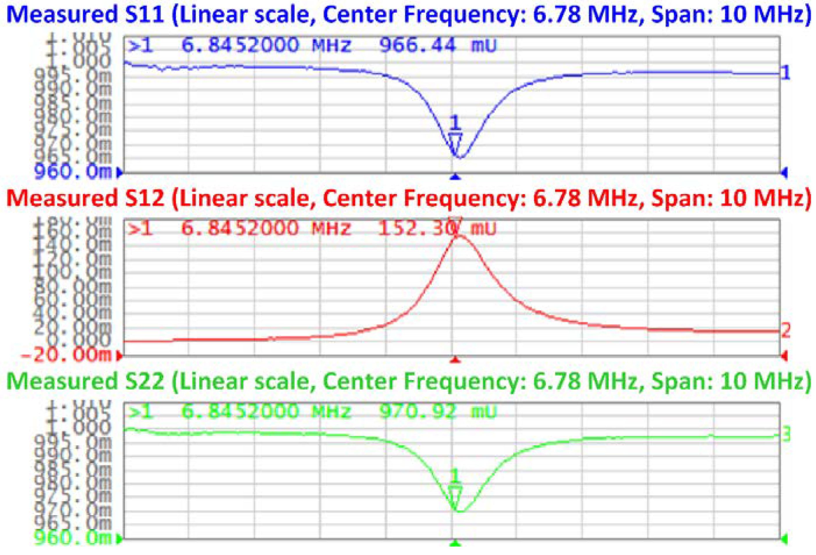
From the full-wave simulation results, an efficiency in excess of 81% was expected for a 50-W power transfer. To experimentally evaluate the fabricated coils, they were tuned using ceramic capacitors. The resulting tuned frequencies of the coils were measured using a network analyzer, E5061B (Keysight). Figure 8 shows the measured magnitude of the scattering parameters (S-parameters) of the transmitter and the receiver coils when they were 60 cm away from each other. S11 (blue line) and S22 (green line) had their minimum values at the tuned frequency, 6.87 MHz. S21 (red line), the transmission coefficient, was also maximized at the tuned frequency. This tuned frequency was 1.3% higher than the target frequency of 6.78 MHz, but this tuning frequency error was ignored in the experiment because the error has a negligible impact on the peak power transfer efficiency as shown in Figure 9 and Figure 10. Moreover, a GaN-based H-bridge inverter that will be explained in a following section could adjust its output frequency in 0.01-MHz steps.
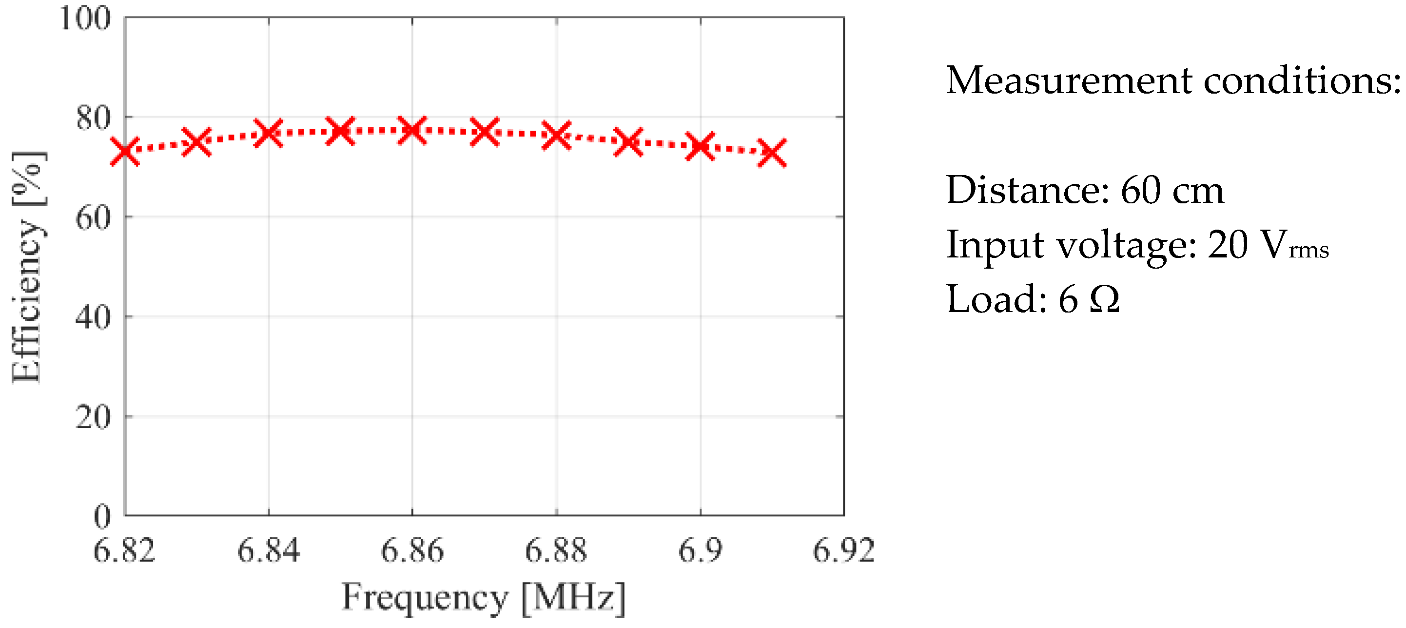
The coil-to-coil efficiency was measured using two different tests. The first measurement was performed using the E5061B and its real-time WPT coil analysis software that can simulate coil-to-coil efficiency in real-time with arbitrary load settings based on the measured S-parameters of the resonant coils [32]. Using the S-parameters of the coils, the input and output power, efficiency, and the input impedance of the coil-to-coil system were simulated in real-time. The simulation results are shown in Figure 9. The blue and red lines show the input and the output power of the coils when the input voltage of the transmitter coil is set to 20 Vrms and a virtual load of 6 Ω is connected to the receiver coil. As shown in the figure, the peak power transfer efficiency was approximately 77% when the operating frequency was 6.87 MHz with input and output powers of 84 W and 65 W, respectively. This result was a little lower than the FEA results in Figure 5b. This is because the measured ESRs of the coils were a little higher than the simulated results of the FEA as shown in Figure 7.
The coil-to-coil efficiency was evaluated experimentally as well. Using a variable frequency H-bridge inverter, the power transfer efficiency between the transmitter and the receiver coils was measured at various frequencies. In regard to the measurement of the coil-to-coil efficiency, an oscilloscope (HDO8108A, TeledyneLecroy, Chestnut Ridge, NY, USA) with a 12-bit ADC resolution, 10 GS/s sample rate, 1 GHz bandwidth, a differential voltage probe (HVD3605A, TeledyneLecroy, Chestnut Ridge, NY, USA) and a current probe (CP031, TeledyneLecroy, Chestnut Ridge, NY, USA) with a measurement bandwidth of 100 MHz (14 times higher than 6.87 MHz) were used. The measured efficiency is plotted in Figure 10. A peak power transfer efficiency occurred when the operating frequency was 6.86 MHz, which was very close to the result in Figure 9. The peak value was 77%, which was very similar to the real-time simulated results in Figure 9. These results demonstrate the validity of the coil design and fabrication methodologies described in Section 3.1 and Section 3.3.
4. 6.78-MHz, 100-W, 92% Efficiency H-Bridge Inverter
In order to supply 50 W using the 77% efficient transmitter and receiver coils, the development of a high efficiency, 6.78-MHz, 100-W, H-bridge inverter was investigated. Four GS61004B, 100-V, 35-A, enhancement mode HEMT (High-electron-mobility transistor) GaN switches (GaN Systems, Ottawa, ON, Canada), and two TI’s LM5113 half-bridge drivers (TI, Dallas, TX, USA) were used. A TI’s 32-bit microcontroller, TMS320F28377S (TI, Dallas, TX, USA), was used as a gate signal generator and a power controller. The details of the developed inverter are presented in the following sections.
4.1. PCB Layout
After multiple failures in an attempt to develop a high-frequency inverter, the authors discovered that the PCB layout of the driver and GaN switches were the most important factors in determining its performance. Two features are of notable importance in the PCB design. The first is a parasitic inductance between the gate driver and the GaN switch. Due to the high operating frequency (6.78 MHz), parasitic inductances between the gate drivers and the switches form resonance circuits with the input capacitances of the GaN switches. This resulted in unwanted ringing of the gate drive signal. This ringing caused undesirable on/off and failures of the GaN switches.
The second aspect to be considered is a heat dissipation of the GaN switches to achieve high power generation (100 W) compared to the size of the switch package. The GS61004B switch was designed to sink heat to the bottom side of its package, especially through its source pad. Per its datasheet, the required PCB pattern under its source and drain pin is over 25 × 25 mm2 for optimum heat dissipation. However, this large pad requirement leads to a large gap between the gate driver and the GaN switch and resulted in a large parasitic inductance between the driver and switch. Figure 11a shows the initial PCB layout of the inverter that focused on the heat dissipation of the four switches. In this initial design, the PCB pattern under the source pin of the switches was 25 mm × 25 mm. To avoid additional thermal burden on the PCB, the gate drivers (LM5113) were positioned 4 cm away from the GaN switches. However, this 4-cm separation caused significant ringing of the gate drive signal and the operation of the GaN switches was not stable even at 0.5 MHz.
Figure 11b shows a revised version of the inverter. The gate drivers were placed 0.8 cm above the switches and only 5 mm × 5 mm of the PCB pattern was allocated to the source pin of the high-side GaN switch. With this compact layout of the driver and switches, the gate signal ringing problem was eliminated. However, the revised version did not allocate sufficient pad area for heat dissipation of the switches. Instead of a large pad, a heat sink was installed at the bottom layer of the PCB in this revised version. The ground plane at the bottom layer of the PCB was uncovered as shown in Figure 11c. The generated heat from the switches and gate drivers was transferred to this bottom plane and cooled using a heat sink that was assembled with a fan (see Figure 11d). A thermal image of the fabricated inverter is shown in Figure 11e. The maximum temperature rise of the GaN switch’s package was 15 °C compared to its initial temperature when the inverter output power was 81 W. Figure 12 shows a measured input and output voltages and currents of the inverter with 25 Vrms input voltage and 6 Ω load. The measured input power was 88 W and output power was 81 W. Therefore, the efficiency of the resonant inverter was 92%.
4.2. Switch Control
The gate drive signals of the inverter were digitally controlled using a TI’s 200-MHz, 32-bit microcontroller unit (MCU), TMS320F28377S. The resolution of a PWM (Pulse width modulation) module of the MCU was 5 ns when the system clock was 200 MHz. The PWM module was able to generate pulses with periods of 145 ns (6.67 MHz) or 150 ns (6.89 MHz) with a single count change. PWM signals in the frequency range of 6.67 MHz to 6.89 MHz could not be generated. However, the target WPT system had very high Q coils and the transmitted power and efficiency were very sensitive to the operating frequency as shown in Figure 9. Therefore, the regular PWM module was not suitable for 6.78-MHz operation. Instead of the regular PWM module, a high-resolution pulse width modulation (HRPWM) module capable of enhancing the resolution of the PWM to 180 ps was used for fine adjustment of the PWM frequency. Using the HRPWM, it was possible to change the operating frequency in 0.01-MHz steps. Phase-shift control and frequency control of the inverter switches were easily implemented using the MCU. Figure 13 shows a photo of the entire assembled inverter board.
5. Receiver Side Full-Wave Rectifier Design
The series-tuned receiver coil was coupled to a full-bridge rectifier. The rectifier diodes were 100-V, 8-A, Schottky barrier diodes (PMEG100V080ELPD from NXP, Eindhoven, Netherlands) with a 10-ns reverse recovery time when the forward current is 0.5 A. To minimize unwanted parasitic inductances and capacitances that can alter the tuning frequency of the RX coil, four diodes were placed very close to the BNC terminals. Two low-side diodes were connected on top of the PCB and high-side diodes were connected at the bottom of the PCB as shown in Figure 14a. Multiple ceramic capacitors and two polymer aluminum capacitors were used as a filter. The diodes were designed for heat dissipation through its cathode pad. Therefore, a heat sink was installed at the rectifier’s positive DC plane as shown in Figure 14b.
6. Experimental Evaluation
6.1. Experimental Setup
Figure 15 shows a configuration of the test-bed. The H-bridge inverter was connected to the transmitter resonant tank through a coaxial cable (16 AWG, American wire guage) with a BNC termination. Also, the receiver coil was connected to the diode rectifier with the same coaxial cable and termination. A Chroma’s DC electronic load, 63102 (Chroma, Foothill Ranch, CA, USA) was used with a constant resistor mode setting.
Figure 16 shows a photo of the entire test-bed. Instead of the DC electronic load, two 20-W, 12-V DC light bulbs were connected to the rectifier’s output terminal to demonstrate wireless energy transmission over 60 cm. Using this test-bed, the power transfer efficiency at various distances, load power, and operating frequency was measured.
6.2. Efficiency Analysis of the Developed System
Figure 17 shows the measured input DC voltage and current of the H-bridge inverter and output DC voltage and current of the rectifier when the load resistance was 6 Ω. Because the efficiency was maximized when the operating frequency was 6.86 MHz, the switching frequency of the inverter was 6.86 MHz. The measured output power was 47.1 W while the measured input power was 82.3 W. Therefore, the measured DC-to-DC power transfer efficiency was 57%. This result was relatively low compared to the measured efficiency between the coils which was 77% at its rated operation.
For a loss analysis of the developed system, the efficiency of every component of the system was measured and denoted in Figure 15. It was found that additional losses were coming from the 16 AWG coaxial cables. This is a notable point since a coaxial cable of only 10 cm in length had a comparable power transfer efficiency to the inverter and the rectifier. Although the cross-sectional area of the coaxial cable (1.3 mm2) was sufficient to carry a 5-Arms transmitter current at low frequencies, it was not appropriate to carry the same current at 6.78 MHz.
Figure 18 shows the estimated loss percentages of the developed system. The conduction losses of the H-bridge inverter and the RX side rectifier were calculated using RDS(on) (37 mΩ) and the forward voltage drop of the rectifying diodes based on their datasheet. The switching loss of the inverter was calculated by subtracting the conduction loss from the total loss associated with the inverter. The losses of the transmitter and receiver coils were calculated using their measured resistance and measured root-mean-square (RMS) of the currents of the coils. It should be noted that the losses of the transmitter and receiver coils overwhelmed other losses. The switching loss of the inverter was second largest loss in the developed system. Therefore, the coil design and fabrication method were key in improving the efficiency of this loosely-coupled WPT system. To evaluate the effectiveness of the developed system on large distance power transmission, efficiency values were measured at various distances of the transmitter and the receiver coils. The distance was increased from 60 cm to 80 cm in 5-cm steps.
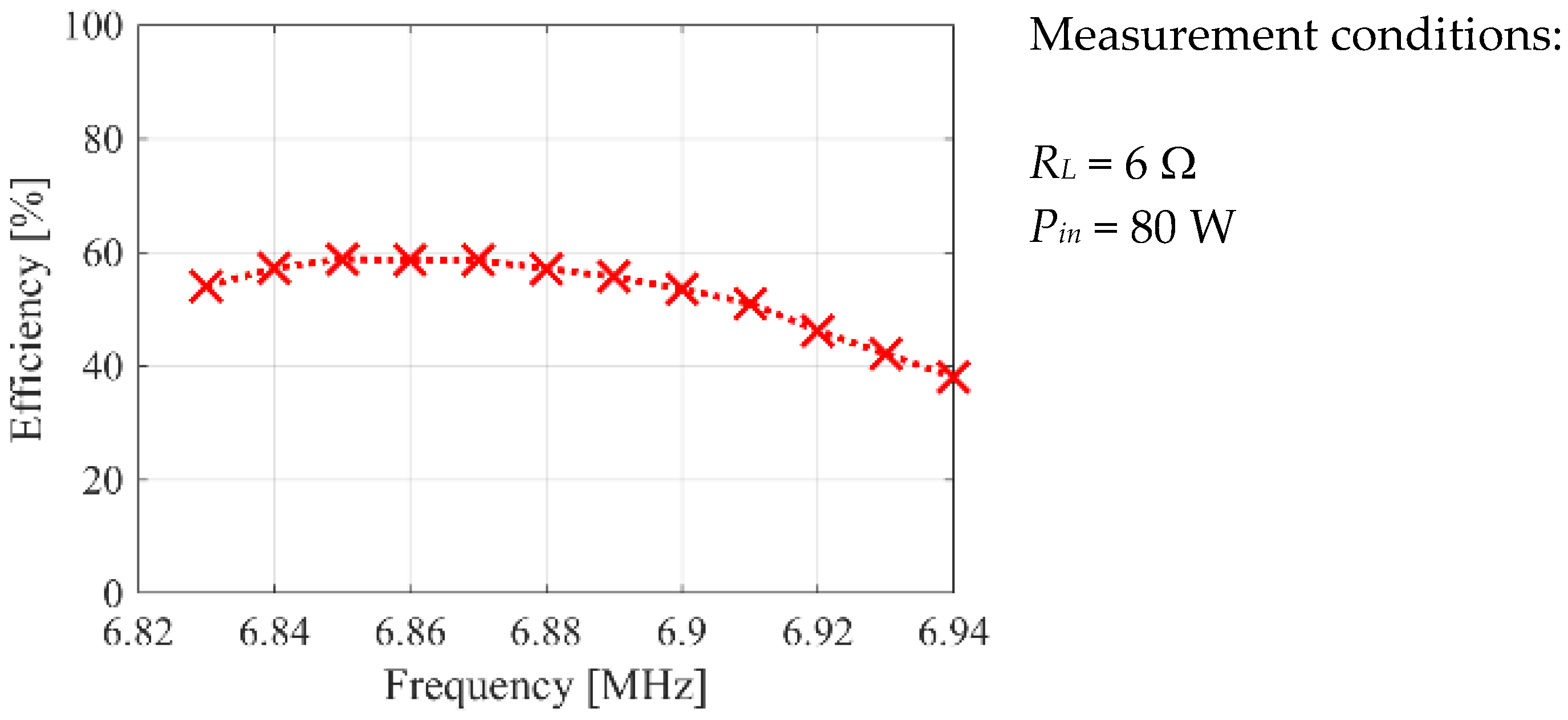
Figure 19 shows the measured efficiencies when the load was 6 Ω, the input power was 80 W, and the operating frequency was 6.86 MHz. When the distance was 60 cm, the efficiency was 57%. However, this value monotonically decreased to 29% when the distance was 80 cm. It is notable that the total efficiency is reduced by approximately 7% for every 5-cm increase in the distance of the coils. This shows that the efficiency of the proposed system is sensitive to the distance of the coils. For this outdoor large air-gap WPT system, appropriate fixtures and installation guidelines are required to prevent a significant degradation of its performance due to wind and other severe weather conditions. The impact of the operating frequency on the efficiency of the test-bed was also evaluated as shown in Figure 20. The measured overall efficiency was also maximized when the operating frequency was 6.86 MHz. The efficiency decreased as the operating frequency moved away from the tuned frequency. The efficiency was decreased to 38% when the operating frequency was 6.94 MHz. This is 0.08 MHz higher than the tuned frequency. This result demonstrates that fine control of the inverter operating frequency is a critical factor of power transfer efficiency.
Finally, the impact of load resistance on the efficiency of the system was evaluated. Figure 21 shows the result of an efficiency vs. load resistance plot. When the load resistance has a rated value RL = 6 Ω, the power transfer efficiency is maximized to 57%. As the load resistance increased or decreased, the power transfer efficiency decreased, and the efficiency is only 35% when the load resistance is 30 Ω. This plot shows that there is an optimal load resistance for a maximum power transmission.
7. Conclusions
In this paper, a new 6.78-MHz, 50-W, over 60 cm wireless power transfer system is proposed. The design and fabrication methodologies for the coils, a GaN-based 6.78-MHz H-bridge inverter, and a rectifier were explained. Using a multi-objective optimization method, Pareto optimality, the transmitter and the receiver coil were determined to a 4-turn and a 5-turn, 40 cm × 40 cm square coils. The selected transmitter and receiver coils were fabricated on a PCB. It was shown that the dielectric loss of the PCB substrate can dominate Ohmic loss of copper traces at MHz frequencies. A PCB substrate with very low dissipation factor was used to reduce the dielectric loss of the coils. The fabricated coils had over 350 Q-factors at 6.78 MHz. The peak coil-to-coil efficiency for the WPT system was 77% at 60 cm air-gap.
In addition, a 6.78-MHz, 100-W, 92% efficiency, GaN-based H-bridge inverter was developed. Two important points were considered in the development of the inverter: a low parasitic inductance of the gate drive circuit and a good heat dissipation of the GaN switch at its rated output power. Parasitic inductances between the gate drivers and GaN switches caused significant ringing of the on/off signals and poor operation performances even at sub-MHz frequencies. A close positioning of the gate driver to the switch was the key for 6.78-MHz operation. However, the congregating of the gate drivers and switches was inferior in cooling and heat dissipation of the inverter. To resolve the thermal issues, the ground plane at the bottom of the PCB was uncovered, and a heatsink with a fan was attached to the PCB. The fabricated 6.78-MHz resonant inverter had a 92% efficiency and the peak temperature was lower than 45 °C at its rated output. Using a high-resolution PWM module of the TI’s MCU, the switching signals could be changed in 0.01-MHz steps. This was very helpful in fine tuning of the high Q-factor coils. Using a full-wave rectifier that was built using four Schottky barrier diodes, the induced voltage and current of the receiver coil were converted to DC values.
The measured DC-to-DC efficiency of the developed WPT system was 57% when the output power was 47 W. The efficiencies of individual components of the system were measured and lossy parts were identified. The impacts of the coil distance, operating frequency, and load resistance on the power transfer efficiency were also evaluated. As the distance increased from 60 cm to 80 cm, the efficiency decreased from 57% to 29% (about a half of the initial value). Therefore, the distance was important in the efficiency of the WPT system. Also, the efficiency decreased from 57% to 38% when the operating frequency was increased from 6.86 MHz to 6.94 MHz (a change of only 0.08 MHz). Finally, the dependence of efficiency on the load resistance was tested. It was shown that there was an optimal load value that maximizes the efficiency, and this value was determined to be 6 Ω, which corresponds to the target-rated load resistance of the developed system.
Author Contributions
Conceptualization, S.-H.L. and M.-Y.K.; methodology, S.-H.L. and M.-Y.K.; software analysis, K.-P.Y.; validation, S.-H.L., K.-P.Y., and M.-Y.K..; formal analysis, S.-H.L.; investigation, M.-Y.K., writing—original draft preparation, S.-H.L.; writing—review and editing, K.-P.Y. and M.-Y.K.; supervision, M.-Y.K..; project administration, S.-H.L. and K.-P.Y.; funding acquisition, S.-H.L. and M.-Y.K..
Funding
This research was supported by the 2016 Research Fund of the University of Seoul awarded to Seung-Hwan Lee. This work was also supported by a grant (18RTRP-B097048-04) from the Railroad Technology Development Program funded by Ministry of Land, Infrastructure and Transport (MOLIT) of Korean government and Korea Agency for Infrastructure Technology Advancement (KAIA) awarded Kyung-Pyo Yi and Myung-Yong Kim.
Conflicts of Interest
The authors declare no conflict of interest.
References
- RamRakhyani, A.K.; Mirabbasi, S.; Chiao, M. Design and Optimization of Resonance-Based Efficient Wireless Power Delivery Systems for Biomedical Implants. IEEE Trans. Biomed. Circuits Syst. 2011, 5, 48–63. [Google Scholar] [CrossRef] [PubMed]
- Salim, A.; Baldi, A.; Ziaie, B. Inductive link modeling and design guidelines for optimum power transfer in implantable wireless microsystems. In Proceedings of the 25th Annual International Conference of the IEEE Engineering in Medicine and Biology Society (IEEE Cat. No. 03CH37439), Cancun, Mexico, 17–21 September 2003; Volume 4, pp. 3368–3371. [Google Scholar]
- Lenaerts, B.; Puers, R. An inductive power link for a wireless endoscope. Biosens. Bioelectron. 2007, 22, 1390–1395. [Google Scholar] [CrossRef] [PubMed]
- Ko, Y.D.; Jang, Y.J. The optimal system design of the online electric vehicle utilizing wireless power transmission technology. IEEE Trans. Intell. Transp. Syst. 2013, 14, 1255–1265. [Google Scholar] [CrossRef]
- Kim, J.H.; Lee, B.S.; Lee, J.H.; Lee, S.H.; Park, C.B.; Jung, S.M.; Lee, S.G.; Yi, K.P.; Baek, J. Development of 1-MW Inductive Power Transfer System for a High-Speed Train. IEEE Trans. Ind. Electron. 2015, 62, 6242–6250. [Google Scholar] [CrossRef]
- Guidi, G.; Suul, J.A.; Jenset, F.; Sorfonn, I. Wireless Charging for Ships: High-Power Inductive Charging for Battery Electric and Plug-In Hybrid Vessels. IEEE Electrif. Mag. 2017, 5, 22–32. [Google Scholar] [CrossRef]
- Lee, S.H.; Kim, J.H.; Lee, J.H. Development of a 60 kHz, 180 kW, over 85% efficiency inductive power transfer system for a tram. Energies 2016, 9, 1075. [Google Scholar] [CrossRef]
- Wang, Z.; Wei, X.; Dai, H. Design and Control of a 3 kW Wireless Power Transfer System for Electric Vehicles. Energies 2015, 9, 10. [Google Scholar] [CrossRef]
- Park, Y.; Cho, Y.H.; Lee, K.; Jung, H.; Kim, H.; Kwon, S.; Park, H. Development of an FPGA-based Online Condition Monitoring System for Railway Catenary Application. In Proceedings of the World Congress on Railway Research (WCRR), Seoul, Korea, 18–22 May 2008; p. 143. [Google Scholar]
- Korea Rail Network Authority. Railway Design Guidelines and Handbooks: Guidace on Overhead Line Clearances (KR E-03140); Korea Rail Network Authority: Daejeon, Korea, 2012. [Google Scholar]
- Lee, S.-H.; Lee, J.-H.; Yi, K.-P. A New Design Methodology for a 1 Meter Distance, 6.78 MHz Wireless Power Supply System for Telemetries. In Proceedings of the IEEE Energy Conversion Congress and Exposition, ECCE 2016, Milwaukee, WI, USA, 18–22 September 2016. [Google Scholar]
- Lee, S.-H.; Yi, K.-P. Development of 50 W High Quality Factor Printed Circuit Board Coils for a 6.78 MHz, 60 cm Air-gap Wireless Power Transfer System. J. Korean Soc. Railw. 2016, 19, 468–479. [Google Scholar] [CrossRef]
- Lee, S.-H. Design Methodologies for Low Flux Density, High Efficiency, kW Level Wireless Power Transfer Systems with Large Air Gaps. Ph.D. Dissertation, University of Wisconsin-Madison, Madison, WI, USA, 2013. [Google Scholar]
- AirFuelAllience. AirFuel Resonant Wireless Power Transfer (WPT) System Baseline System Specifications; AirFuelAllience: Beaverton, OR, USA, 2017. [Google Scholar]
- Sample, A.P.; Meyer, D.A.; Smith, J.R.; Member, S.; Meyer, D.A.; Smith, J.R. Analysis, Experimental Results, and Range Adaptation of Magnetically Coupled Resonators for Wireless Power Transfer. IEEE Trans. Ind. Electron. 2011, 58, 544–554. [Google Scholar] [CrossRef]
- Duong, T.P.; Lee, J.-W. Experimental Results of High-Efficiency Resonant Coupling Wireless Power Transfer Using a Variable Coupling Method. IEEE Microw. Wirel. Compon. Lett. 2011, 21, 442–444. [Google Scholar] [CrossRef]
- Lee, S.-H.; Lorenz, R.D. A Design Methodology for Multi-kW, Large Airgap, MHz Frequency, Wireless Power Transfer Systems. In Proceedings of the IEEE Energy Conversion Congress and Exposition: Energy Conversion Innovation for a Clean Energy Future (ECCE 2011), Phoenix, AZ, USA, 17–22 September 2011. [Google Scholar]
- Calder, R.J.; Lee, S.H.; Lorenz, R.D. Efficient, MHz Frequency, Resonant Converter for Sub-Meter (30 cm) Distance Wireless Power Transfer. In Proceedings of the 2013 IEEE Energy Conversion Congress and Exposition, ECCE 2013, Denver, CO, USA, 15–19 September 2013; pp. 1917–1924. [Google Scholar]
- Akuzawa, Y.; Tsuji, K.; Matsumori, H.; Ito, Y.; Ezoe, T.; Sakai, K. A 95% Efficient Inverter with 300-W Power Output for 6.78-MHz Magnetic Resonant Wireless Power Transfer System. In Proceedings of the 2015 IEEE MTT-S International Microwave Symposium, Phoenix, AZ, USA, 17–22 May 2015; pp. 60–62. [Google Scholar]
- Sakai, K.; Ito, Y.; Ezoe, T.; Akuzawa, Y. A 99%-Efficiency GaN Converter for 6.78 MHz Magnetic Resonant Wireless Power Transfer System. J. Eng. 2014, 2014, 598–600. [Google Scholar]
- Yang, J.-R.; Kim, J.; Park, Y.-J. Class E Power Amplifiers using High-Q Inductors for Loosely Coupled Wireless Power Transfer System. J. Electr. Eng. Technol. 2014, 9, 569–575. [Google Scholar] [CrossRef] [Green Version]
- Narayanamoorthi, R.; Juliet, A.V.; Chokkalingam, B.; Padmanaban, S.; Leonowicz, Z.M. Class E Power Amplifier Design and Optimization for the Capacitive Coupled Wireless Power Transfer System in Biomedical Implants. Energies 2017, 10, 1409. [Google Scholar]
- Grebennikov, A. Load Network Design Techniques for Class E RF and Microwave Amplifier. High Freq. Electron. 2004, 3, 18–32. [Google Scholar]
- Zhao, C.; Costinett, D. GaN-Based Dual-Mode Wireless Power Transfer Using Multifrequency Programmed. IEEE Trans. Ind. Electron. 2017, 64, 9165–9176. [Google Scholar] [CrossRef]
- Bonache-Samaniego, R.; Olalla, C.; Martinez-Salamero, L.; Maksimovic, D. 6.78 MHz Self-Oscillating Parallel Resonant Converter Based on GaN Technology. In Proceedings of the 2017 IEEE Applied Power Electronics Conference and Exposition (APEC), Tampa, FL, USA, 26–30 March 2017; pp. 1594–1599. [Google Scholar]
- Xue, L.; Zhang, J. Single-stage 6.78 MHz Power-Amplifier Design using High-Voltage GaN Power ICs for Wireless Charging Applications. In Proceedings of the 2017 IEEE Applied Power Electronics Conference and Exposition (APEC), Tampa, FL, USA, 26–30 March 2017; pp. 3743–3750. [Google Scholar]
- Ngatchou, P.; Zarei, A.; El-Sharkawi, A.; El-Sharkawi, M.A. Pareto Multi Objective Optimization. In Proceedings of the 13th International Conference on Intelligent Systems Application to Power Systems, Arlington, VA, USA, 6–10 November 2005; pp. 84–91. [Google Scholar]
- Lee, S.H.; Lee, B.S.; Lee, J.H. A New Design Methodology for A 300-Kw, Low Flux Density, Large Air Gap, Online Wireless Power Transfer System. IEEE Trans. Ind. Appl. 2016, 52, 4234–4242. [Google Scholar] [CrossRef]
- Fotopoulou, K.; Flynn, B.W. Wireless Power Transfer in Loosely Coupled Links: Coil Misalignment Model. IEEE Trans. Magn. 2011, 47, 416–430. [Google Scholar] [CrossRef]
- Isola IS680. Available online: http://www.isola-group.com/products/all-printed-circuit-materials/is680/ (accessed on 3 August 2018).
- Mohan, S.S.; Hershenson, M.D.M.; Boyd, S.P.; Lee, T.H. Simple Accurate Expressions for Planar Spiral Inductances. IEEE J. Solid-State Circuits 1999, 34, 1419–1420. [Google Scholar] [CrossRef]
- Keysight E5061B-006 Wireless Power Transfer Analysis. Available online: https://www.keysight.com/en/pd-2571977-pn-E5061B/wireless-power-transfer-analysis?cc=US&lc=eng (accessed on 19 August 2018).
Figure 1.
Configurations of the target catenary monitoring system and the WPT system: (a) Target system configuration; (b) Block diagram of the wireless power transfer system.
Figure 1.
Configurations of the target catenary monitoring system and the WPT system: (a) Target system configuration; (b) Block diagram of the wireless power transfer system.


Figure 2.
Geometric design parameters of the square coils.

Figure 3.
H-field calculation diagram.

Figure 4.
Pareto front of the WPT system.

Figure 5.
Finite element simulation model and simulated efficiencies: (a) FEA model; (b) Simulated efficiency.
Figure 5.
Finite element simulation model and simulated efficiencies: (a) FEA model; (b) Simulated efficiency.

Figure 6.
Configuration of the WPT system: (a) Dielectric loss density-FR4; (b) Dielectric loss density-IS680.
Figure 6.
Configuration of the WPT system: (a) Dielectric loss density-FR4; (b) Dielectric loss density-IS680.

Figure 7.
Photos of transmitter and receiver coils: (a) Top of transmitter coil; (b) Bottom of transmitter coil; (c) Top of receiver coil; (d) Bottom of receiver coil.
Figure 7.
Photos of transmitter and receiver coils: (a) Top of transmitter coil; (b) Bottom of transmitter coil; (c) Top of receiver coil; (d) Bottom of receiver coil.

Figure 8.
Measured S-parameters of the transmitter and receiver coils.

Figure 9.
Real-time simulation results using Keysight’s WPT analysis software (with 20 Vrms input voltage and 6 Ω load resistance setting).
Figure 9.
Real-time simulation results using Keysight’s WPT analysis software (with 20 Vrms input voltage and 6 Ω load resistance setting).

Figure 10.
Measured coil-to-coil efficiency with 6 Ω load resistor.

Figure 11.
Configuration of the WPT system: (a) Initial design; (b) Revised design; (c) Fabricated inverter; (d) Bottom side ground plane; (e) Assembled heatsink and a fan; (f) Thermal image of the inverter at 81-W output.
Figure 11.
Configuration of the WPT system: (a) Initial design; (b) Revised design; (c) Fabricated inverter; (d) Bottom side ground plane; (e) Assembled heatsink and a fan; (f) Thermal image of the inverter at 81-W output.

Figure 12.
Input and output power of the H-bridge inverter. Measurement conditions: distance: 60 cm, input voltage: 25 Vrms, load: 6 Ω.
Figure 12.
Input and output power of the H-bridge inverter. Measurement conditions: distance: 60 cm, input voltage: 25 Vrms, load: 6 Ω.

Figure 13.
A photo of the assembled H-bridge inverter.

Figure 14.
Photos of full-wave rectifier: (a) Top-view (b) Side-view.

Figure 15.
Configuration of the test-bed.

Figure 16.
A photo of the experimental setup.

Figure 17.
Measured input and output DC voltages and currents at the rated output power. Measurement conditions: distance: 60 cm, operating frequency = 6.86 MHz, load: 6 Ω.
Figure 17.
Measured input and output DC voltages and currents at the rated output power. Measurement conditions: distance: 60 cm, operating frequency = 6.86 MHz, load: 6 Ω.

Figure 18.
Estimated percentage losses of the developed system.

Figure 19.
Efficiency dependent on distance.

Figure 20.
Efficiency dependence on frequency.

Figure 21.
Efficiency dependence on load resistance.


Table 1.
Design spans of transmitter and receiver coils.
| Parameters | Design Limits | Parameters | Design Limits |
|---|---|---|---|
| Inner diameter, | 10–30 cm | Trace width, w | 1–2.5 cm |
| Turn spacing, s | 0.5–2 cm | # of turns, n | 1–8 turns |
Table 2.
Selected design of the transmitter and receiver coils.
| Parameters | Transmitter Coil | Receiver Coil |
|---|---|---|
| Inner diameter | 18 cm | 12 cm |
| Outer diameter | 39.8 cm | 39.6 cm |
| Turn spacing, s | 0.7 cm | 0.7 cm |
| Trace width, w | 2.2 cm | 2.2 cm |
| Trace thickness | 71 μm | 71 μm |
| Number of turns, n | 4 | 5 |
| Substrate thickness | 1.6 mm | 1.6 mm |
Table 3.
Comparison of material properties of FR-4 and IS680.
| Parameters | FR-4 | IS680 |
|---|---|---|
| Relative permittivity | 4.8 | 3.2 |
| Loss tangent | 0.017 | 0.0032 |
| Dielectric strength | 20 kV/mm | 30 kV/mm |
| Thermal conductivity | 0.29 W/m/K | 0.32 W/m/K |
Table 4.
Circuit parameters of the designed coils at 6.78 MHz.
| Circuit Parameters | Theoretical | FEA Results | Measurement | |||
|---|---|---|---|---|---|---|
| TX | RX | TX | RX | TX | RX | |
| Self-inductance [μH] | 6.67 | 7.15 | 6.5 | 7.53 | 6.24 | 7.2 |
| AC resistance [Ω] | 0.31 | 0.38 | 0.48 | 0.70 | 0.58 | 0.81 |
| Q-factor @ 6.78 MHz | 916 | 801 | 576 | 458 | 458 | 379 |
| Mutual-inductance [μH] | 0.11 | 0.11 | 0.09 | |||
| Coupling coefficient | 0.016 | 0.016 | 0.013 | |||
© 2019 by the authors. Licensee MDPI, Basel, Switzerland. This article is an open access article distributed under the terms and conditions of the Creative Commons Attribution (CC BY) license (http://creativecommons.org/licenses/by/4.0/).
Share and Cite
MDPI and ACS Style
Lee, S.-H.; Yi, K.-P.; Kim, M.-Y. 6.78-MHz, 50-W Wireless Power Supply Over a 60-cm Distance Using a GaN-Based Full-Bridge Inverter. Energies 2019, 12, 371. https://doi.org/10.3390/en12030371
AMA Style
Lee S-H, Yi K-P, Kim M-Y. 6.78-MHz, 50-W Wireless Power Supply Over a 60-cm Distance Using a GaN-Based Full-Bridge Inverter. Energies. 2019; 12(3):371. https://doi.org/10.3390/en12030371
Chicago/Turabian StyleLee, Seung-Hwan, Kyung-Pyo Yi, and Myung-Yong Kim. 2019. "6.78-MHz, 50-W Wireless Power Supply Over a 60-cm Distance Using a GaN-Based Full-Bridge Inverter" Energies 12, no. 3: 371. https://doi.org/10.3390/en12030371
Note that from the first issue of 2016, this journal uses article numbers instead of page numbers. See further details here.