High-Efficiency Design and Control of Zeta Inverter for Single-Phase Grid-Connected Applications


Division of Electronic Engineering, Chonbuk National University, Jeonju 561-756, Korea
*
Author to whom correspondence should be addressed.
Energies 2019, 12(6), 974; https://doi.org/10.3390/en12060974
Submission received: 13 February 2019
/
Revised: 8 March 2019
/
Accepted: 11 March 2019
/
Published: 13 March 2019
(This article belongs to the Special Issue Design and Control of Power Converters 2019)
Abstract
:The conventional zeta inverter has been used for single-phase grid-connected applications. However, it has high switching losses to operate at high switching frequency in the continuous conduction mode (CCM). To address this drawback, this paper suggests a high-efficiency zeta inverter using active clamp and synchronous rectification techniques. The proposed inverter utilizes the active clamp circuit for reducing switching losses. The non-complementary switching scheme is adopted for not only clamping the switch voltage stresses, but also alleviating the circulating energy. In addition, the synchronous rectification is implemented for reducing the body diode conduction of power switches. By using the silicon carbide (SiC) metal oxide semiconductor field effect transistors (MOSFETs), the switching performance of the proposed inverter is improved. Its operation principle and control strategy are presented. A 220-W prototype has been designed and tested to evaluate the performance of the proposed inverter.
1. Introduction
With the fast growth of renewable energy markets, many single-stage isolated inverters have been developed for single-phase grid-connected applications [1,2,3,4,5,6,7,8,9]. Among them, the zeta inverter [7,8,9] has been gaining attention due to the advantages of its low grid current ripple and low circuit component count, compared to other single-stage inverters such as flyback inverters [1,2,3,4] and Cuk inverters [5,6]. Of course, although the zeta inverter has large current ripples at the dc side, similar to the flyback inverter, it has been widely adopted for single-phase photovoltaic applications [7,8,9] due to its simple and flexible circuitry.
As the zeta inverter operates at a constant switching frequency, it has two operation modes: discontinuous conduction mode (DCM) and continuous conduction mode (CCM). The DCM zeta inverter has been used for low-power applications [7]. The grid current is easily controlled, as its control transfer function for the grid current is linear in DCM [8]. However, as the power level increases, the DCM zeta inverter suffers from high conduction losses. The DCM zeta inverters need to be connected in parallel to alleviate conduction losses.
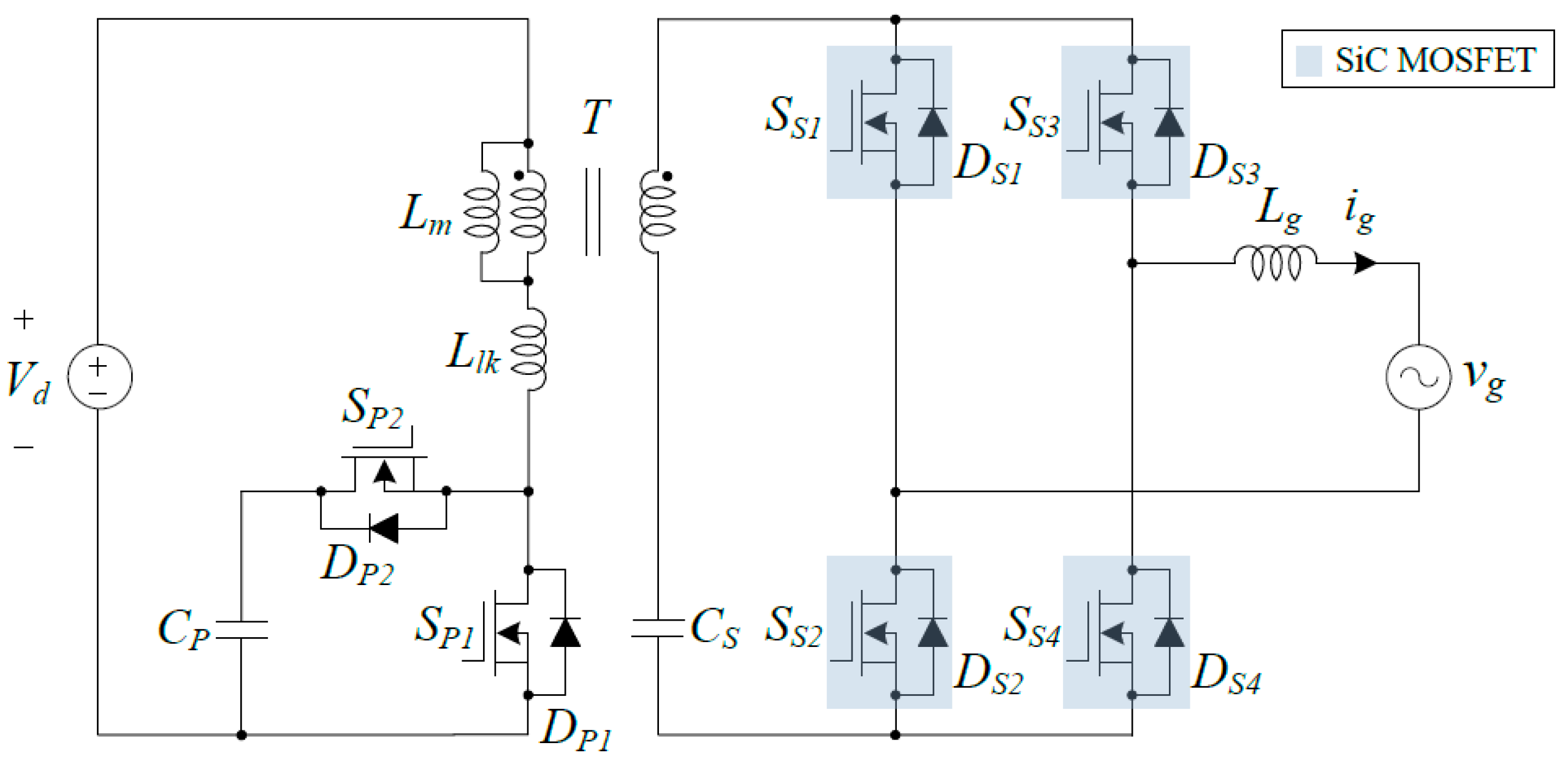
When the zeta inverter operates in CCM, it can withstand a higher power level than the DCM zeta inverter. The CCM zeta inverter has been suggested in [9]. Figure 1 shows its circuit diagram, which is equivalent to the circuit diagram in [9]. It consists of the primary circuit (SP1, Lm, Llk) and the secondary circuit (CS, SS1 ~ SS4, Lg). T is a high-frequency transformer, which has the magnetizing inductor Lm and the leakage inductor Llk. The CCM zeta inverter has achieved higher efficiency than the DCM zeta inverter by lowering conduction losses [9]. However, the CCM zeta inverter suffers from high switching losses. In the primary circuit, the switch SP1 operates at a high switching frequency to regulate the grid current ig. When SP1 is turned off, a high voltage spike is generated due to the energy stored in the leakage inductor Llk, which increases switching losses [10].
The secondary circuit provides the current path to fold the grid voltage vg and gives the freewheeling path for the grid current ig. The switches SS1 ~ SS4 operate at grid frequency according to the polarity of vg. SS2 and SS3 are always turned on for the positive grid cycle, while SS1 and SS4 are always turned on for the negative grid cycle. For the positive grid cycle, when SP1 is turned on, ig flows through SS2 and SS3. As SP1 is turned off, ig flows through SS2, SS3, DS1, and DS4. DS1 and DS4 are the body diodes, which are turned on for the freewheeling of ig. However, when SP1 is turned on again, DS1 and DS4 are not turned off instantly due to the slow reverse recovery process [11]. The reverse recovery currents of DS1 and DS4 cause high voltage spikes across DS1 and DS4. They are also transferred to the primary circuit, which increases the turn-on switching losses of SP1. It is worse when high-voltage silicon (Si) metal oxide semiconductor field effect transistors (MOSFETs) are adopted, because their body diodes have poor reverse recovery characteristics. These drawbacks limit the practical use of the CCM zeta inverter, despite its advantages.
This paper proposes a high-efficiency zeta inverter to cope with the above-mentioned drawbacks. Figure 2 shows the circuit diagram of the proposed inverter. The active clamp circuit has been used for reducing switching losses in the primary circuit. The active clamp circuit has the auxiliary switch SP2 and the clamp capacitor CP. Conventionally, the auxiliary switch SP2 operates complementary to the main switch SP1 [12]. As the energy stored in Llk is absorbed in CP, the switch voltages are clamped to a constant voltage. However, this conventional method increases the circulating current in the primary circuit. It causes additional power losses due to high circulating energy. To address this drawback, the non-complementary switching scheme [13] has been adopted. In the non-complementary method, SP2 is turned on for a short time before SP1 is turned on. As the leakage energy is recycled with reduced circulating current, power losses associated with the circulating energy can be minimized in the proposed inverter.
In the secondary circuit, the synchronous rectification [14] is used for reducing the body diode conduction of MOSFETs. With synchronous rectification, SS1 (SS2) and SS4 (SS3) are turned on for the positive (negative) grid cycle when SP1 is turned off. It allows ig to freewheel through the MOSFET channels instead of the body diodes. It avoids the body diode conduction, increasing the power efficiency, because the voltage drop across the on-state resistance of the MOSFET is lower than the forward voltage drop of the body diode [15]. The silicon carbide (SiC) MOSFET has been utilized for the synchronous rectification of SS1 ~ SS4. Due to the advantages over Si MOSFETs such as wider bandgap and higher electric field capacity [16], it improves the switching performance of the proposed inverter.
This paper is organized as follows. Section 2 describes the operation principle of the proposed inverter in the steady-state condition, along with the analysis of active clamp and synchronous rectification techniques. It also describes the control strategy for the CCM operation of the proposed inverter. Section 3 discusses the experimental results to verify the performance of the proposed inverter. Section 4 presents the conclusion of this paper.
2. Proposed Inverter
2.1. Operation Principle
Figure 3 shows the circuit diagram of the proposed inverter, which shows the reference directions of currents and voltages. The proposed inverter consists of the primary circuit (SP1, SP2, CP, Lm, Llk) and the secondary circuit (CS, SS1 ~ SS4, Lg). The active clamp circuit consists of SP2 and CP. T is a high-frequency transformer, which has the magnetizing inductor Lm and the leakage inductor Llk. It is assumed that Lm >> Llk. Its turns ratio n is NS / NP. NP is the primary winding turns. NS is the secondary winding turns. All of the power switches are considered ideal except for their body diodes. Vd is the dc input voltage. vg is the grid voltage. Lm and Lg are large enough so that the currents iLm and ig are continuous during one switching period Ts, respectively. CP and CS are large enough so that the voltages VCp and VCs are constant during Ts, respectively. VCs is considered as ǀvgǀ because the secondary circuit provides the current path to fold vg.
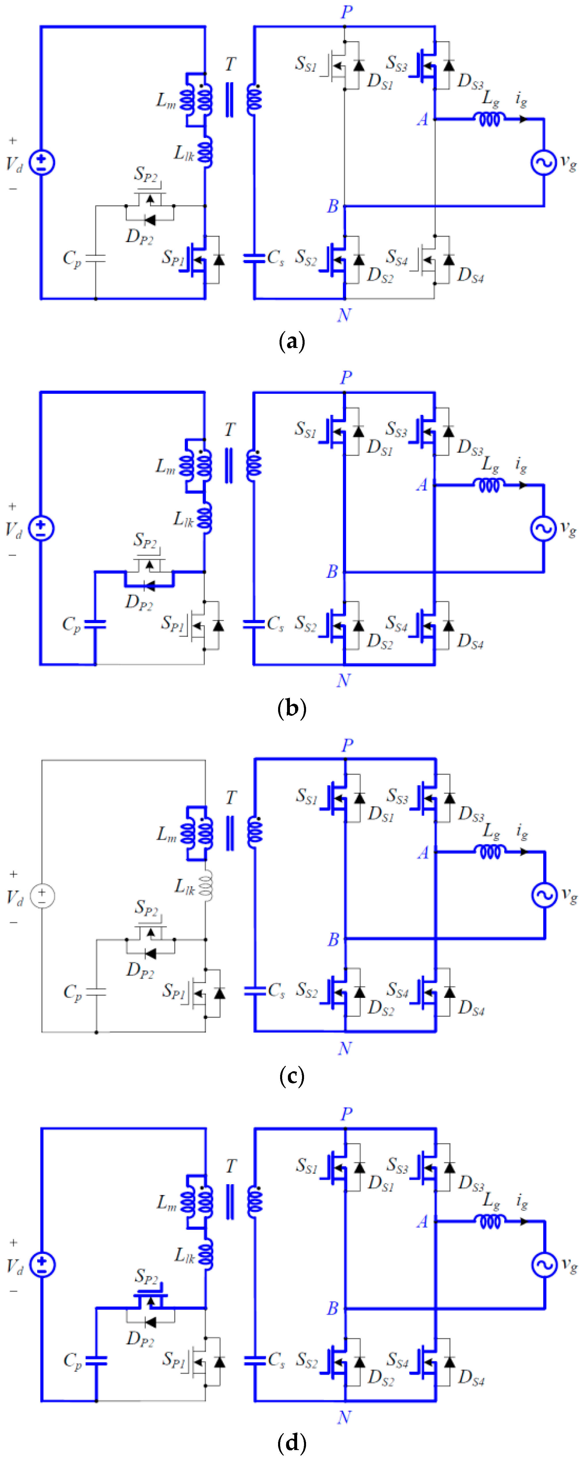
Figure 4 shows the switching circuit diagrams of the proposed inverter during Ts for the positive grid cycle. Figure 5 shows the switching waveform diagrams of the proposed inverter during Ts for the positive grid cycle. Vgate,P1 and Vgate,P2 are the gate signals for SP1 and SP2, respectively. Vgate,S1 ~ Vgate,S4 are the gate signals for SS1 ~ SS4, respectively. SP1 and SP2 operate with a constant high switching frequency fs (= 1/Ts). SP2 is turned on for a short time before SP1 is turned on. For the positive grid cycle, SS2 and SS3 are always turned on. SS1 and SS4 operate complementary to SP1. The proposed inverter has four switching modes during Ts for the positive grid cycle, which are outlined below.
Mode 1 [to–t1]: At t = to, SP1 is turned on. Lm and Llk store the energy from Vd. iLm increases linearly at the rate of diLm /dt = Vd /(Lm + Llk). The voltage across the secondary winding of T is nLmVd /(Lm + Llk). ig increases linearly at the rate of dig /dt = nLmVd /(Lm + Llk) /Lg.
Mode 2 [t1–t2]: At t = t1, DP2 is turned on as SP1 is turned off. The energy stored in Llk is stored in CP. The switch voltage VP1 is clamped to VCp. SS1 and SS4 are turned on in this mode. As the voltage across the secondary winding of T is vg, iLm decreases linearly at the rate of diLm /dt = −vg /nLm. As ig freewheels through SS1 ~ SS4, ig decreases linearly at the rate of dig /dt = −vg /Lg.
Mode 3 [t2–t3]: At t = t2, DP2 is turned off as iCp becomes zero. The switch voltage VP1 is clamped to Vd + vg /n. The switch voltage VP2 is clamped to VCp + Vd + vg /n. iLm and ig keep decreasing linearly as in Mode 2.
Mode 4 [t3–t4]: At t = t3, SP2 is turned on for transferring the energy stored in CP to the grid. The absorbed leakage energy is recycled to the grid. The switch voltage VP1 is clamped to VCp. iLm and ig keep decreasing linearly as in Mode 2.
From Mode 2 to Mode 4, the following current relations are obtained as iCs = −iS1 − iS3 = −iS2 − iS4 and ig = iS2 − iS1 = iS4 − iS3 with respect to the nodes P, N, A, and B. Next, the switching cycle begins as SP1 is turned on, and SP2, SS1, and SS4 are turned off. For the negative grid cycle, SS1 and SS4 are always turned on. SS2 and SS3 operate complementary to SP1. The operation principle for the negative grid cycle is not described here, because it can be explained analogously as the operation principle for the positive grid cycle.
2.2. Active Clamp Circuit
In the active clamp circuit, SP2 is turned on for a short period before SP1 is turned on. The absorbed leakage energy is recycled as the energy stored in CP is transferred to the grid. Figure 6 shows the detailed timing diagrams for Vgate,P1, Vgate,P2, and iCp. TON is the turn-on time of SP1. TOFF is the turn-off time of SP1. TDP2 is the turn-on time of DP2. TSP2 is the turn-on time of SP2. As SP2 is turned on, the capacitor current iCp can be represented as:
By the charge balance for the capacitor CP during Ts, the areas A and B for two current waveforms should be equal to:
where iP1,PK is the peak value of iP1. Supposing that TDP2 = TSP2, the capacitor voltage VCp is represented as:
Also, the circulating energy ECir during TSP2 is represented as:
The circulating energy ECir will be smaller as TSP2 is getting shorter. However, in the active clamp method using the complementary switching scheme [12], the circulating energy is related with the turn-off time TOFF, which is much longer than TSP2. Thus, the non-complementary switching scheme results in higher power efficiency by reducing the circulating energy.
2.3. Synchronous Rectification with SiC MOSFETs
Figure 7 shows the detailed switching circuit diagrams for the operation principle of the secondary circuit for the positive grid cycle. Figure 7a shows the switching circuit diagram of the secondary circuit in the previous inverter in Figure 1. ig freewheels through the body diodes DS1 and DS4 when SP1 is turned off. When SP1 is turned on, DS1 and DS4 are not turned off immediately because of the slow reverse recovery process [11]. Then, the diode reverse recovery currents cause high voltage spikes across DS1 and DS4. Also, the diode reverse recovery currents are transferred to the primary circuit through the transformer, which causes high current spikes for SP1. On the other hand, Figure 7b shows the switching circuit diagram of the secondary circuit in the proposed inverter. When SP1 is turned off, SS1 and SS4 are turned on. ig freewheels through the MOSFET channels instead of the body diodes, which minimizes the conduction of the body diodes. When SP1 is turned on again, SS1 and SS4 are turned off without the reverse recovery process of the body diodes.
When SS1 and SS4 are turned off, the voltage across the secondary winding of T is nLmVd /(Lm + Llk). The switch voltage stresses VS1 and VS4 are represented as:
The switch voltage stresses VS2 and VS3 are identical to VS1 and VS4 in Equation (5). Suppose that the system parameters are given as Vd = 48 V, n = 4.5, and vg = 220 Vrms with negligible leakage inductor. The switch voltage stress is approximately calculated as 527 V without considering any voltage oscillations. Practically, the use of high voltage (>700 V) MOSFETs is inevitable to withstand the switch voltage stresses for a high switching frequency. However, when Si MOSFETs are adopted for SS1 ~ SS4, the proposed inverter will suffer from high conduction losses due to the high on-state resistances of Si MOSFETs. Thus, the SiC MOSFET is an attractive alternative to the Si MOSFET for high-frequency and high-voltage applications. Due to its advantages over Si MOSFETs such as its wider bandgap and higher electric field capacity, it improves the switching performance of the proposed inverter, increasing the power efficiency.
2.4. Control Strategy
Supposing that the leakage inductor is negligible, the volt-second balance for Lg during Ts gives the following voltage equation as:
where D is the duty cycle of SP1. By rearranging Equation (6), we have the relation between vg and Vd as:
Assuming no power losses in the inverter circuit, we have the relation between id and ig as:
where id is the input current. Suppose that CP keeps the charge balance, id is considered as iP1 during Ts. Then, the following current relations are represented as:
where k is a proportional factor. From equations (8) and (9), we have the relation between iLm and ig as:
The average voltage for Lm during Ts can be represented with respect to the deviation ∆iLm of iLm as:
From Equation (11), D can be represented as:
By using equations (7) and (10), D in Equation (12) can be written as:
where Dn is the nominal duty cycle, and Dc is the control duty cycle as:
Vg is the absolute peak value of vg. ω is the angular frequency of vg. Supposing that vg is measured exactly with a phase-locked loop (PLL) [17], Dn plays the role of providing the nominal voltage compensation. By using Dn, the non-linear system in Equation (11) is transformed to the first-order linear system, which can be controlled by the control duty cycle Dc. In order to regulate the grid current ig with low harmonic currents, Dc is implemented by a proportional-resonant (PR) control [18] whose ideal transfer function CPR (s) is:
where kp and kr are the PR control gains, respectively. However, it is unable to realize the PR controller in Equation (15) with an infinite gain. Thus, the following non-ideal transfer function is adopted in practice as:
where ωc is the angular frequency at the cutoff frequency of the controller. In addition, the harmonic compensators can be added to the PR controller to minimize the harmonic currents for the selective harmonic frequencies [19]. Its transfer function CHC (s) is expressed as:
where h is the harmonic order and krh is the resonant control gain for each harmonic frequency. Since the third, fifth, and seventh harmonics are significant under the grid environment, the third to seventh harmonic compensators are implemented. The harmonic compensators provide high gains at the selected harmonic frequencies, helping minimize the steady-state error and the disturbance by the selected frequency components. Figure 8 shows the control block diagram of the proposed inverter. I*g is the peak magnitude of the current reference i*g. The duty cycle D is generated by summing Dn and Dc.
3. Experimental Results
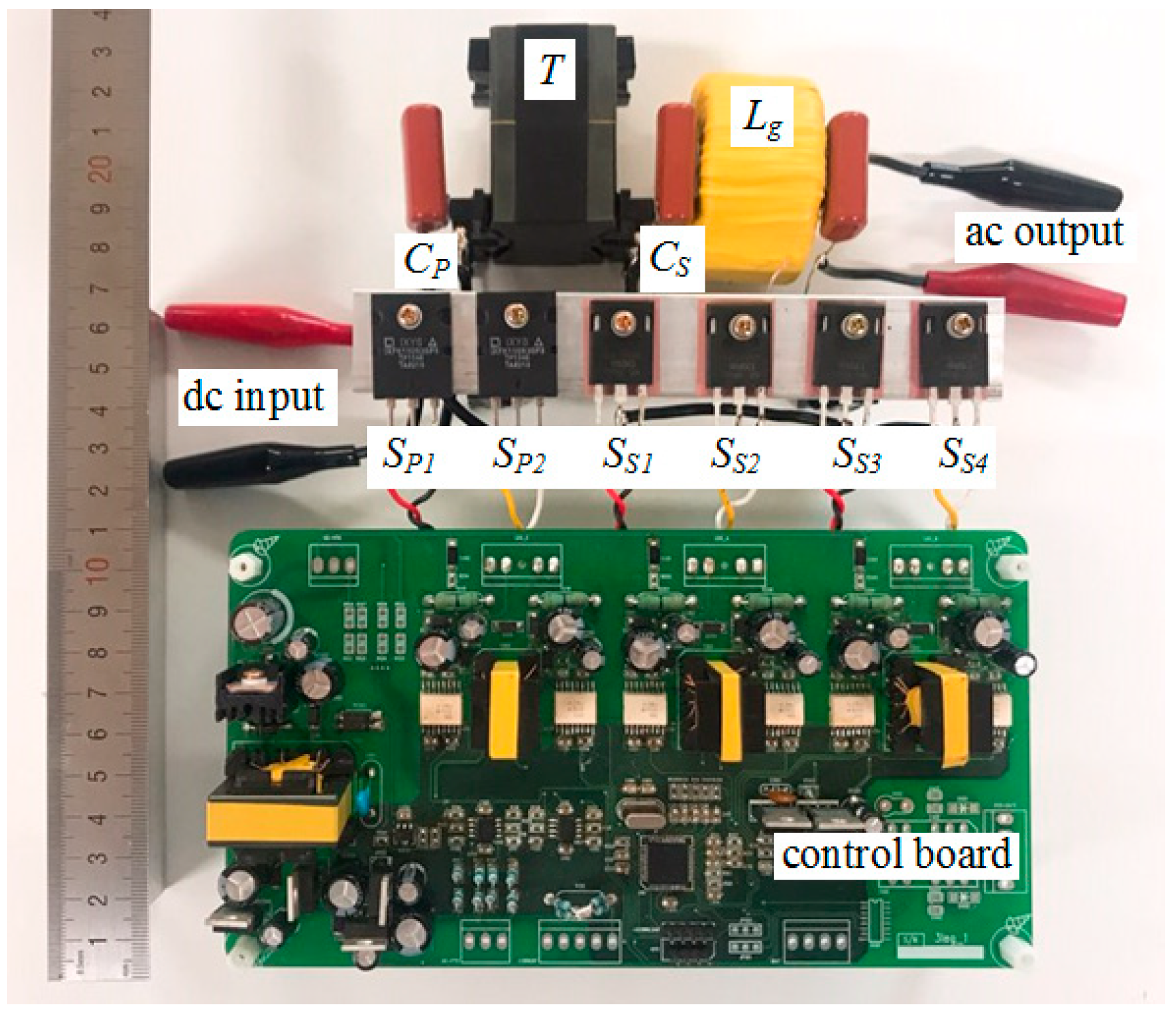
A 220-W prototype system has been designed and tested to evaluate the performance of the proposed inverter. Table 1 shows the system parameters and the circuit components. As a SiC MOSFET, UJC1206k (UnitedSiC) has been used for SS1 ~ SS4. As a digital signal controller, dsPIC30F6015 (Microchip) has been used for implementing the current controller and generating the duty cycle signals for all of the power switches. Figure 9 shows the picture of the prototype system. The prototype system includes the power circuit and the control circuit. Even though it is not optimized for the commercialized level, it is expected that the proposed inverter could achieve high power density if it is implemented with advanced devices such as gallium nitride (GaN) devices [20] and planar transformers [21].
The proposed inverter has been simulated to verify its operation principle. It has been simulated by the physical security information management (PSIM) software for the system parameters in Table 1. Figure 10 shows the simulation waveforms of the proposed inverter. The steady state operation of the proposed inverter can be verified from Figure 10a–d. Figure 10e,f show the simulation waveforms of the proposed inverter in the transient state condition. Figure 10e shows vg and ig as the output power changes from 110 W to 220 W. Figure 10f shows vg and ig as the output power changes from 220 W to 110 W.
Figure 11 shows the experimental waveforms of the previous inverter in Figure 1. The previous inverter has been designed and tested for the same system parameters as the proposed inverter. It uses the same circuit components in Table 1, except that STW40N95K5 (STMicroelectronics), as a Si MOSFET, has been adopted for SS1 ~ SS4. Figure 11a shows the gate signal Vgate,P1 and the switch voltage VP1 for SP1. When SP1 is turned off, VP1 has a high voltage spike, which results from the energy stored in the transformer leakage inductor. Figure 11b shows the gate signal Vgate,P1 and the switch current iP1 for SP1. When SP1 is turned on, iP1 has a high current spike, which results from the reverse recovery current of the body diodes in the secondary circuit.
Figure 12 shows the experimental waveforms of the proposed inverter. Figure 12a shows Vgate,P1, Vgate,P2, and VP1. Figure 12b shows Vgate,P1, Vgate,P2, and VP2. As shown in Figure 12a,b, VP1 and VP2 are maximally clamped to the capacitor voltage VCp. Figure 12c shows Vgate,P1, Vgate,P2, and iP1. The switch current iP1 in Figure 12c has lower current spike than the switch current iP1 in Figure 11b because of the synchronous rectification of the secondary circuit. Figure 12d shows Vgate,P1, Vgate,P2, and iCp. It is observed that the capacitor charging and discharging currents are well balanced in the proposed inverter.
Figure 13 shows the experimental waveforms in the secondary circuit for the positive grid cycle. Figure 13a shows VS1 in the previous inverter. It is observed that there is high voltage oscillation across SS1, which results from the slow reverse recovery process of the body diode of the Si MOSFET. Figure 13b shows Vgate,S1 and VS1 in the proposed inverter. With synchronous rectification, the SiC MOSFET channel has been used for the rectification. It is shown that voltage oscillation across SS1 has been much alleviated due to the fast switching operation of the SiC MOSFET. The switch currents iS1, iS2, iS3, and iS4 are shown from Figure 13c–f with respect to ig in the proposed inverter.
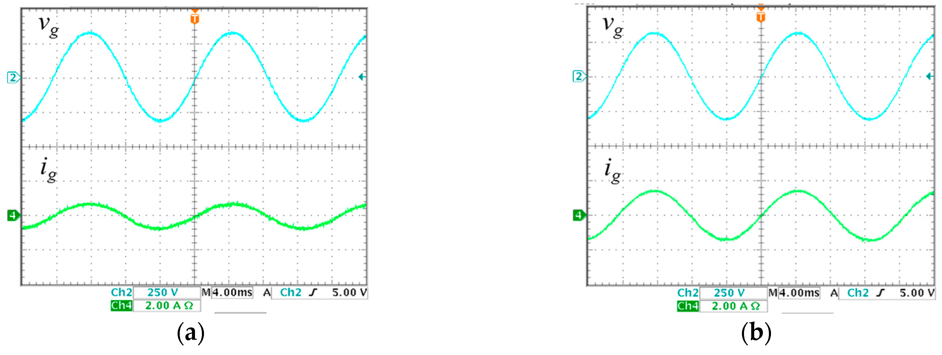
Figure 14 shows the experimental waveforms of the proposed inverter. Figure 14a shows vg and ig as the proposed inverter supplies 110 W into the grid. Figure 14b shows vg and ig as the proposed inverter supplies 220 W into the grid. As ig is in phase with vg, the power factor is measured as 0.99 in Figure 14.
Figure 15 shows the measured power efficiency curves. The curve A shows the measured power efficiency of the previous inverter. It has achieved the peak efficiency of 93.5% at the rated power. The curve B shows the measured power efficiency of the proposed inverter when the synchronous rectification has been implemented without the active clamp circuit. The proposed inverter has improved the power efficiency, achieving the peak efficiency of 94.2% at the rated power. The curve C shows the measured power efficiency of the proposed inverter when both active clamp and synchronous rectification techniques have been implemented. The proposed inverter has achieved the peak efficiency of 95.0% at the rated power by using active clamp and synchronous rectification techniques.
Figure 16a shows the measured power efficiency curves up to 440 W. The prototype system has shown the peak efficiency of 95.0% at 220 W. The efficiency decreases gradually as the output power level goes up from 300 W to 440 W. The prototype system has achieved the efficiency of 94.3% at 440 W. Figure 16b shows the measured power efficiency curves for 50 kHz and 100 kHz, respectively. As the switching frequency increases, the power efficiency decreases because of the switching losses. In order to improve the power efficiency and the power density further, the circuit design scheme should be advanced by considering the GaN devices [20] and the planar transformers [21] for megahertz operations.
4. Conclusions
This paper has proposed a high-efficiency zeta inverter using active clamp and synchronous rectification techniques for single-phase grid-connected applications. The operation principle of the proposed inverter has been described. The active clamp and synchronous techniques adopted in the proposed inverter have been explained. The non-complementary switching scheme has been applied to the active clamp circuit. It effectively reduces the switching losses and circulating current in the primary circuit. The synchronous rectification with SiC MOSFETs alleviates switching losses in the secondary circuit. The control strategy for the CCM operation of the proposed inverter has been presented. A 220-W prototype system has been designed and tested to evaluate the performance of the proposed inverter. Experimental results have shown that the proposed inverter has improved the power efficiency by reducing switching losses, compared to the previous inverter.
Author Contributions
W.-Y.C. managed the project and wrote the manuscript. M.-K.Y. performed the experiments, analyzed the data, and edited the manuscript.
Funding
This research was supported by the National Research Foundation of Korea (NRF-2016R1D1A3B03932350). Also, it was supported by research funds of Chonbuk National University in 2018.
Conflicts of Interest
The authors declare no potential conflict of interest.
References
- Dong, D.; Agamy, M.S.; Harfman-Todorovic, M.; Liu, X.; Garces, L.; Zhou, R.; Cioffi, P. A PV residential microinverter with grid-support function: Design, implementation, and field testing. IEEE Trans. Ind. Appl. 2018, 54, 469–481. [Google Scholar] [CrossRef]
- Hu, H.; Harb, S.; Kutkut, N.H.; Shen, Z.H.; Batarseh, I. A single-stage microinverter without using electrolytic capacitors. IEEE Trans. Power Electron. 2013, 28, 2677–2687. [Google Scholar] [CrossRef]
- Feng, X.; Wang, F.; Wu, C.; Luo, J.; Zhang, L. Modeling and comparisons of aggregated flyback microinverters in aspect of harmonic resonances with the grid. IEEE Trans. Ind. Electron. 2019, 66, 276–285. [Google Scholar] [CrossRef]
- Lodh, T.; Pragallapati, N.; Agarwal, V. Novel control scheme for an interleaved flyback converter based solar PV microinverter to achieve high efficiency. IEEE Trans. Ind. Appl. 2018, 54, 3473–3482. [Google Scholar] [CrossRef]
- Han, B.; Lee, J.S.; Kim, M.S. Repetitive controller with phase-lead compensation for Cuk CCM inverter. IEEE Trans. Ind. Electron. 2018, 65, 2356–2367. [Google Scholar] [CrossRef]
- Han, B.; Lai, J.-S.; Kim, M.S. Dynamic modeling and controller design of dual-mode Cuk inverter in grid-connected PV/TE applications. IEEE Trans. Power Electron. 2018, 33, 8887–8904. [Google Scholar] [CrossRef]
- Levin, G.H.; Flores, J.V.; Salton, A.; dos Reis, F.S. Internal model control of the zeta converter for the grid connection of photovoltaic panels. In Proceedings of the Brazilian Power Electronics Conference, Gramado, Brazil, 27–31 October 2013; pp. 666–671. [Google Scholar]
- Viero, R.C.; Lopez, H.F.M.; Zollmann, C.A.; dos Reis, F.S. Dynamic modeling of a sinusoidal inverter based on zeta converter working in DCM for PV arrays. In Proceedings of the Annual Conference on IEEE Industrial Electronics Society (IECON), Glendale, AZ, USA, 7–10 November 2010; pp. 439–444. [Google Scholar]
- Surapaneni, R.K.; Rathore, A.K. A single-stage CCM zeta microinverter for solar photovoltaic AC module. IEEE J. Emerg. Sel. Top. Power Electron. 2015, 3, 892–900. [Google Scholar] [CrossRef]
- Murthy-Bellur, D.; Kazimierczuk, M.K. Isolated two-transistor zeta converter with reduced transistor voltage stress. IEEE Trans. Circuits Syst. II Express Briefs 2011, 58, 41–45. [Google Scholar] [CrossRef]
- Brown, C.D.; Sarlioglu, B. Reducing switching losses in BLDC motor drives by reducing body diode conduction of MOSFETs. IEEE Trans. Ind. Appl. 2015, 51, 1864–1871. [Google Scholar] [CrossRef]
- Chen, M.; Sun, J. Reduced-order averaged modeling of active-clamp converters. IEEE Trans. Power Electron. 2006, 21, 487–494. [Google Scholar] [CrossRef]
- Zhang, J.; Huang, X.; Wu, X.; Qian, Z. A high efficiency flyback converter with new active clamp technique. IEEE Trans. Power Electron. 2010, 25, 1775–1785. [Google Scholar] [CrossRef]
- Yin, S.; Liu, Y.; Liu, Y.; Tseng, K.J.; Pou, J.; Simanjorang, R. Comparison of SiC voltage source inverters using synchronous rectification and freewheeling diode. IEEE Trans. Ind. Electron. 2018, 65, 1051–1061. [Google Scholar] [CrossRef]
- Mohammadi, M.; Ordonez, M. Synchronous rectification of LLC resonant converters using homopolarity cycle modulation. IEEE Trans. Ind. Electron. 2019, 66, 1781–1790. [Google Scholar] [CrossRef]
- Jordán, J.; Esteve, V.; Sanchis-Kilders, E.; Dede, E.J.; Maset, E.; Ejea, J.B.; Ferreres, A. A comparative performance study of a 1200 V Si and SiC MOSFET intrinsic diode on an induction heating inverter. IEEE Trans. Power Electron. 2014, 29, 2550–2562. [Google Scholar] [CrossRef]
- Han, Y.; Luo, M.; Zhao, X.; Guerrero, J.M.; Xu, L. Comparative performance evaluation of orthogonal-signal-generators-based single-phase PLL algorithms—A survey. IEEE Trans. Power Electron. 2016, 31, 3932–3944. [Google Scholar] [CrossRef]
- Zmood, D.N.; Holmes, D.G. Stationary frame current regulation of PWM inverters with zero steady-state error. IEEE Trans. Power Electron. 2003, 18, 814–822. [Google Scholar] [CrossRef]
- Pereira, L.F.A.; Flores, J.V.; Bonan, G.; Coutinho, D.F.; da Silva, J.M.G. Multiple resonant controllers for uninterruptible power supplies-a systematic robust control design approach. IEEE Trans. Ind. Electron. 2014, 61, 1528–1538. [Google Scholar] [CrossRef]
- Zhang, W.; Huang, X.; Liu, Z.; Lee, F.C.; She, S.; Du, W.; Li, Q. A new package of high-voltage cascade gallium nitride device for megahertz operation. IEEE Trans. Power Electron. 2016, 31, 1344–1353. [Google Scholar] [CrossRef]
- Zhao, S.; Li, Q.; Lee, F.C.; Li, B. High-frequency transformer design for modular power conversion from medium-voltage AC to 400 VDC. IEEE Trans. Power Electron. 2018, 33, 7545–7557. [Google Scholar] [CrossRef]
Figure 1.
Circuit diagram of the zeta inverter.

Figure 2.
Circuit diagram of the proposed inverter.

Figure 3.
Circuit diagram of the proposed inverter with reference directions of currents and voltages.
Figure 3.
Circuit diagram of the proposed inverter with reference directions of currents and voltages.

Figure 4.
Switching circuit diagrams of the proposed inverter during Ts for the positive grid cycle: (a) Mode 1; (b) Mode 2; (c) Mode 3; and (d) Mode 4.
Figure 4.
Switching circuit diagrams of the proposed inverter during Ts for the positive grid cycle: (a) Mode 1; (b) Mode 2; (c) Mode 3; and (d) Mode 4.

Figure 5.
Switching waveform diagrams of the proposed inverter during Ts for the positive grid cycle.
Figure 5.
Switching waveform diagrams of the proposed inverter during Ts for the positive grid cycle.

Figure 6.
Detailed timing diagrams for Vgate,P1, Vgate,P2, and iCp.

Figure 7.
Detailed switching circuit diagrams for the operation principle of the secondary circuit for the positive grid cycle: (a) previous inverter; and (b) proposed inverter.
Figure 7.
Detailed switching circuit diagrams for the operation principle of the secondary circuit for the positive grid cycle: (a) previous inverter; and (b) proposed inverter.

Figure 8.
Control block diagram of the proposed inverter.

Figure 9.
Picture of the prototype system.

Figure 10.
Simulation waveforms: (a) Vgate,P1, Vgate,P2, VP1, and VP2; (b) Vgate,P1, Vgate,P2, iP1, and iCp; (c) ig, iS2, and iS3; (d) ig, iS1, and iS4; (e) vg and ig from 110 W to 220 W; and (f) vg and ig from 220 W to 110 W.
Figure 10.
Simulation waveforms: (a) Vgate,P1, Vgate,P2, VP1, and VP2; (b) Vgate,P1, Vgate,P2, iP1, and iCp; (c) ig, iS2, and iS3; (d) ig, iS1, and iS4; (e) vg and ig from 110 W to 220 W; and (f) vg and ig from 220 W to 110 W.

Figure 11.
Experimental waveforms of the previous inverter: (a) Vgate,P1 and VP1; and (b) Vgate,P1 and iP1.
Figure 11.
Experimental waveforms of the previous inverter: (a) Vgate,P1 and VP1; and (b) Vgate,P1 and iP1.

Figure 12.
Experimental waveforms of the proposed inverter: (a) Vgate,P1, Vgate,P2, and VP1; (b) Vgate,P1, Vgate,P2, and VP2; (c) Vgate,P1, Vgate,P2, and iP1; and (d) Vgate,P1, Vgate,P2, and iCp.
Figure 12.
Experimental waveforms of the proposed inverter: (a) Vgate,P1, Vgate,P2, and VP1; (b) Vgate,P1, Vgate,P2, and VP2; (c) Vgate,P1, Vgate,P2, and iP1; and (d) Vgate,P1, Vgate,P2, and iCp.

Figure 13.
Experimental waveforms in the secondary circuit for the positive grid cycle: (a) VS1 in the previous inverter; (b) Vgate,S1 and VS1 in the proposed inverter; (c) ig and iS2 in the proposed inverter; (d) ig and iS3 in the proposed inverter; (e) ig and iS1 in the proposed inverter; and (f) ig and iS4 in the proposed inverter.

Figure 14.
Experimental waveforms of the proposed inverter: (a) vg and ig as the proposed inverter supplies 110 W into the grid; and (b) vg and ig as the proposed inverter supplies 220 W into the grid.
Figure 14.
Experimental waveforms of the proposed inverter: (a) vg and ig as the proposed inverter supplies 110 W into the grid; and (b) vg and ig as the proposed inverter supplies 220 W into the grid.

Figure 15.
Measured power efficiency curves.

Figure 16.
Measured power efficiency curves: (a) power efficiency curves up to 440 W; and (b) power efficiency curves for different switching frequencies.
Figure 16.
Measured power efficiency curves: (a) power efficiency curves up to 440 W; and (b) power efficiency curves for different switching frequencies.


Table 1.
System parameters and circuit components.
| Symbol | Quantity | Value |
|---|---|---|
| Vd | dc input voltage | 48 V |
| vg | grid voltage | 60 Hz/220 Vrms |
| fs | switching frequency | 50 kHz |
| Lm | magnetizing inductor | 60 μH |
| Llk | leakage inductor | 0.5 μH |
| NP | primary winding turns | 14 |
| NS | secondary winding turns | 63 |
| CP | clamp capacitor | 1.0 μF |
| SP1, SP2 | primary swiches | IXFK150N30P3 |
| CS | secondary capacitor | 1.0 μF |
| SS1 ~ SS4 | secondary switches | UJC1206K |
| Lg | filter inductor | 2.0 mH |
© 2019 by the authors. Licensee MDPI, Basel, Switzerland. This article is an open access article distributed under the terms and conditions of the Creative Commons Attribution (CC BY) license (http://creativecommons.org/licenses/by/4.0/).
Share and Cite
MDPI and ACS Style
Choi, W.-Y.; Yang, M.-K. High-Efficiency Design and Control of Zeta Inverter for Single-Phase Grid-Connected Applications. Energies 2019, 12, 974. https://doi.org/10.3390/en12060974
AMA Style
Choi W-Y, Yang M-K. High-Efficiency Design and Control of Zeta Inverter for Single-Phase Grid-Connected Applications. Energies. 2019; 12(6):974. https://doi.org/10.3390/en12060974
Chicago/Turabian StyleChoi, Woo-Young, and Min-Kwon Yang. 2019. "High-Efficiency Design and Control of Zeta Inverter for Single-Phase Grid-Connected Applications" Energies 12, no. 6: 974. https://doi.org/10.3390/en12060974
Note that from the first issue of 2016, this journal uses article numbers instead of page numbers. See further details here.