Real-Time Hardware in the Loop Simulation Methodology for Power Converters Using LabVIEW FPGA


1
Electronics Department, Instituto Tecnológico Superior del Sur de Guanajuato, Educación Superior 2000, Benito Juárez, 38980 Uriangato, Guanajuato, Mexico
2
Electronics Department, Tecnológico Nacional de México-IT de Celaya, Antonio García Cubas 600, Fovissste, 38010 Celaya, Guanajuato, Mexico
3
Electronics Technology Department, Universidad Rey Juan Carlos, Calle Tulipán, s/n, 28933 Móstoles, Madrid, Spain
4
Electronics Technology and Communications Department, Universidad Autónoma de Madrid, Ciudad Universitaria de Cantoblanco, 28049 Madrid, Spain
5
Electronics Engineering Department, Tecnológico Nacional de México-CENIDET, Interior Internado, Palmira, 62490 Cuernavaca, Morelos, Mexico
*
Author to whom correspondence should be addressed.
Energies 2020, 13(2), 373; https://doi.org/10.3390/en13020373
Submission received: 27 November 2019
/
Revised: 6 January 2020
/
Accepted: 7 January 2020
/
Published: 13 January 2020
(This article belongs to the Special Issue Advancements in Real-Time Simulation of Power and Energy Systems)
Abstract
:Nowadays, the use of the hardware in the loop (HIL) simulation has gained popularity among researchers all over the world. One of its main applications is the simulation of power electronics converters. However, the equipment designed for this purpose is difficult to acquire for some universities or research centers, so ad-hoc solutions for the implementation of HIL simulation in low-cost hardware for power electronics converters is a novel research topic. However, the information regarding implementation is written at a high technical level and in a specific language that is not easy for non-expert users to understand. In this paper, a systematic methodology using LabVIEW software (LabVIEW 2018) for HIL simulation is shown. A fast and easy implementation of power converter topologies is obtained by means of the differential equations that define each state of the power converter. Five simple steps are considered: designing the converter, modeling the converter, solving the model using a numerical method, programming an off-line simulation of the model using fixed-point representation, and implementing the solution of the model in a Field-Programmable Gate Array (FPGA). This methodology is intended for people with no experience in the use of languages as Very High-Speed Integrated Circuit Hardware Description Language (VHDL) for Real-Time Simulation (RTS) and HIL simulation. In order to prove the methodology’s effectiveness and easiness, two converters were simulated—a buck converter and a three-phase Voltage Source Inverter (VSI)—and compared with the simulation of commercial software (PSIM® v9.0) and a real power converter.
1. Introduction
A hardware in the loop (HIL) simulation is the implementation of a system model in embedded hardware, which represents part of a real system. The main requirement of HIL simulation is that it has to be in real-time [1]. HIL simulation plays a significant role in the development of technology for many applications, presenting advantages such as the short time to market for new products; low cost of prototyping; and risk reduction of damaging test equipment and, more importantly, of harming people during testing.
There are commercial HIL real-time simulators available, such as RTDS® (Winnipeg, MB, Canada), OPAL-RT® (Montreal, QC, Canada), Typhoon® (Somerville, MA, USA), and dSPACE® (Paderborn, Germany), to name a few. The software used by these simulators allows the user to implement the system through a graphical interface; these types of equipment are used for the simulation of complex models and are tools that help designers and engineers all over the world. A review of the state-of-the-art of Real-Time Simulation (RTS) technologies, both hardware and software, is presented in [2]. Many examples of the use of this technology can be found in the literature, including simulating power electronics converters. In [3], the simulation of a Voltage Source Converter (VSC), used in a High Voltage Direct Current (HVDC) system for distributed generation and power quality regulation, is presented. In [4], it is used to test a new sliding mode controller for a standalone system based on photovoltaic (PV) generation. In [5], it is used for evaluating modular multilevel converters. Additionally, in [6], the authors propose an ultralow latency platform for the RTS, which can be used for complex power electronics systems and, as a case study for this particular platform, a driver for a Permanent Magnet Synchronous Generator (PMSG) is simulated. As shown in these references, RTS is employed to test the controller used in power electronics converters and all simulations use a commercial HIL system.
A drawback of these products is their high cost, which can amount to tens of thousands of dollars. As a result, many universities or research centers cannot afford the acquisition of this kind of equipment. Due to this issue, some researchers have developed ad-hoc solutions using low-cost hardware.
For research purposes, three types of hardware are mainly used to achieve RTS: Digital Signal Processors (DSP), Graphic Processing Units (GPU), and Field-Programmable Gate Arrays (FPGA). At present, FPGA is the most used hardware for RTS [7]. The use of FPGA for HIL testing of power converters can be found in the references, such as [8,9,10,11,12,13,14]. This is due to its inherent characteristic of parallel processing, which allows the fast resolution of many equations simultaneously, with short times of integration, in the order of tens of nanoseconds.
Often, the preferred language for the implementation of the system model is Very High-Speed Integrated Circuit Hardware Description Language (VHDL). This language is the best option when the objective is to minimize the FPGA resources and allows the time step to be minimized. However, the use of VHDL requires an expert designer, capable of optimizing the capabilities and the implementation of a proper FPGA application. Some FPGA manufacturers are beginning to offer a more user-friendly Integrated Development Environment (IDE) tool for their FPGA. These IDEs permit the development of FPGA applications using high-level programming languages such as C. In addition, some manufacturers use third-party software, such as MATLAB or LabVIEW, for FPGA applications [15,16]. Some authors have proposed the fast development of power electronics models for HIL simulations using these programs. In [17], the authors develop a new RTS method to test nonlinear control techniques and a methodology to implement the RTS is described, but it is based in a Digital Signal Processor (DSP), which is slower than an FPGA. In [18], the authors propose a methodology for the development of a fast HIL simulation based in MATLAB, but it includes just a small part of the work and is not detailed enough. In [19], the authors suggest fast HIL development based in MATLAB; however, the methodology is only for the design of PV converters. In [20], a high-performance real-time simulator for power electronics based in a novel massively parallel computational engine implemented in low-cost FPGA hardware using VHDL is presented, but there is not enough detail in the implementation. In [21], the HIL implementation of a validation system for an energy management system used in microgrids is presented. This HIL simulation is performed on a PC and has an overall time step of 100 ms, which is slower than the one reached using an FPGA. As a major advantage, the use of a PC means a lower implementation cost.
The company National Instruments (NI) offers reconfigurable industrial controllers, known as Reconfigurable Input Output (RIO) controllers. This platform has huge potential for the development of control systems for power electronics applications and for the development of HIL systems. It is based on an FPGA combined with a microprocessor, although recently, RIO systems were implemented using System on Chip (SoC) technology, which has been demonstrated to work properly in industrial environments.
LabVIEW is the name of the generic NI software development tool. There is a specific module for developing FPGA applications: the LabVIEW FPGA module. It facilitates the generation of FPGA applications using a graphical language that helps non-expert users to create complex and efficient FPGA applications [22].
In this paper, a step-by-step methodology for HIL power converter simulation using the LabVIEW FPGA module is shown. The main difference between this approach and those reported in the literature is that, in the latter, the methodologies used to perform this type of simulation are not clearly explained or do not include enough details for implementation; the advantage of the proposal is that it employs the pipelined technique of LabVIEW and results in a small time step. This methodology is intended to be simple, in order to allow researchers with no experience in languages such as VHDL for RTS to carry out HIL simulations with a reduced cost compared to other tools, but with an accuracy high enough to obtain an appropriate real converter model. In the proposal, LabVIEW is used to allow relatively easy and fast implementation. The methodology consists of five steps: The first step is the design of the power converter; in the second one, the converter model is obtained; during the third step, the model is solved using a numerical method; the fourth step consists of programming an off-line simulation of the model using fixed-point representation; and finally, implementation of the numerical method in the FPGA is conducted. In order to verify the results, a comparison of simulation software such as PSIM, the HIL simulation proposed, and a real converter was carried out using a buck converter and a three-phase voltage source inverter (VSI) as a case study.
2. Proposed Methodology
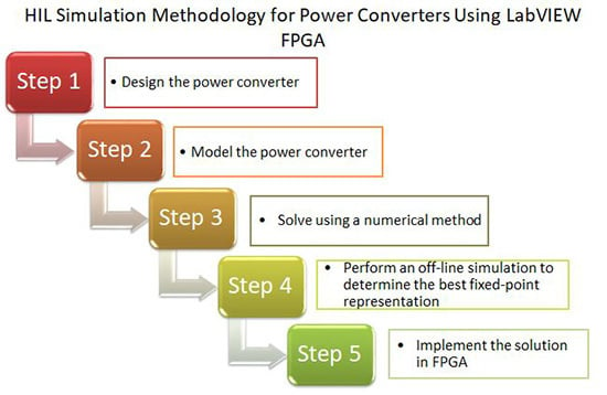
Figure 1 shows the flow diagram of the suggested methodology. As mentioned before, it is composed of five steps. A buck converter and a three-phase VSI are used as a case study. The first step is the design of the converter. Several ways to design both converters can be found in the literature. The second step consists of modeling the power converter. For this purpose, the voltage and current differential equations for every converter switching state are used. In the third step, the differential equations obtained in step two are solved using numerical methods; in this case, by means of the Euler method. During the fourth step, a simulation of the converter using a software tool is carried out, in order to know the best fixed-point representation for the variables involved in the converter, as suggested in [23]. In the last step, FPGA implementation is conducted using the pipelining technique and the single-cycle LabVIEW FPGA mathematical functions. If the simulation result is not satisfactory, the fixed-point representation should be changed and step four should be returned to.
2.1. Power Converter Design (Step One)
As mentioned above, the buck converter (Figure 2a) and three-phase VSI (Figure 2b) were selected to test the methodology. In order to design the buck converter, the steps proposed in [24] were considered. The design parameters of the buck converter and the three-phase VSI are shown in Table 1 and Table 2, respectively, while their calculated passive components are shown in Table 3 and Table 4, respectively.
2.2. Power Converter Modeling (Step Two)
2.2.1. Buck Converter Model
In order to model the converter, the following considerations were made: the switch (S) presents an on-resistance (RDS(ON)) and the diode (D) is considered as a DC voltage when it is conducting (VD). The buck converter presents three switching states, depending on the control signal and the inductor current. The first state occurs when the switch is turned on and the diode is not conducting, the second state starts when the switch is turned off and the diode begins conducting, and the last state is presented when the inductor current is equal to zero. However, when the power converter is working in Continue Conduction Mode (CCM), only the two first states occur. The differential equations are obtained by using Kirchhoff Law’s.
Differential equations for the first state are:
where vC is the capacitor voltage, iL is the inductor current, Vs is the input voltage, R is the load resistance, L is the inductance, RL is the inductance series resistance, C is the capacitance, vo is the output voltage, ESR is the equivalent series resistance of the capacitor, and RDS(ON) is the on-resistance of the switch.
Differential equations for the second state are:
Differential equations for the third state are:
2.2.2. Three-Phase Voltage Source Inverter Model
The three-phase VSI considered in this study is shown in Figure 2b. The following considerations were made in order to simplify the model: in this case, all switches are considered as ideal switches and the inductance series resistance is neglected. Certainly, if a better representation is desired, the non-idealities should be considered. The obtained system model is:
where vxn is the phase ‘x’ inverter voltage, vX is the phase ‘X’ voltage, ix is the phase ‘x’ inverter current, and Lx is the phase ‘x’ inductance.
The inverter output voltage is determined by the switching state or vector applied to the three-phase VSI. Each vector is determined by the switches’ position. It is considered that the control signals of complementary switches of each inverter leg are the opposite, and then just the upper switches’ control signals (s1, s2, and s3) are used in the analysis; a logic 0 means that the device is turned “off” and a logic 1 means that it is turned “on”.
The effective voltage applied by the inverter is obtained considering the common-mode voltage, as follows:
where vxN is the inverter voltage referred to node N and vNn is the common-mode voltage.
The voltage of the inverter referred to the node N is determined by
where sx is the control signal of the switch and VDC is the inverter input DC voltage.
The common-mode voltage is defined as:
Table 5 summarizes the values of the three-phase VSI voltages, depending on the vector applied.
Considering the Equations (4) and (7) and Table 5, the dynamic behavior of the system under a switching state is fully determined. For example, if vector V1 is selected, the following equations are obtained:
A similar procedure may be followed to obtain the equations for any other switching state represented by its corresponding Vx vector.
2.3. Solving the System Using a Numerical Method (Step Three)
In order to solve differential equations like (1)–(3), a numerical method should be used. Many different methods exist. The forward Euler method is used due to its algorithm simplicity, which leads to less use of hardware resources, allows for a smaller time step simulation, and is easy to implement. Convergence and stability are not an issue since the obtained time step is very small, in the order of hundreds of nanoseconds [25]. Some other integration methods, as the 2nd order Runge-Kutta approach, are more complex, resource-demanding, and should imply a more difficult implementation. These factors could be an obstacle for non-expert users or developers. Commercial HIL systems implement basic integration algorithms, such as trapezoidal or backward Euler algorithms, to find a solution [2].
Generally, the numerical solution for a differential equation can be found using the following algorithm:
where yk+1 is the next solution of the method, yk is the current solution of the method, θ is the slope of the differential equation, and h is a fixed time step.
Graphically, the method is shown in Figure 3.
The difference among the mathematical methods is the slope calculation. For the forward Euler method, the first derivative offers a direct estimation of the slope at point tk, so it can be derived as:
The algorithm for the forward Euler method is:
In order to verify the concept, in the following sections, a buck converter case study will be analyzed in detail. A similar approach can be used for the three-phase VSI.
Using (11) to solve Equation (1), the solution for iL(k+1) and vC(k+1) is:
where iL(k+1) is the next inductor current, iL(k) is the present inductor current, vo(k) is the present output voltage, vC(k+1) is the next capacitor voltage, vC(k) is the present capacitor voltage, and Vs(k) is the current input voltage.
The solution of Equation (2) is then:
The solution to Equation (3) is:
These equations can be programmed using any commercial software and using different numerical representations. In this paper, the use of fixed-point representation is strongly recommended since the implementation of a floating-point number in the FPGA is very resource-demanding [26].
2.4. Simulation of the Solution Using a Numerical Method (Step Four)
A simulation of the Equations (12)–(14) using fixed-point representation was carried out in the LabVIEW environment in order to determine the best numeric representation. The following step is the implementation of the discrete model of the buck converter. Its flow diagram is shown in Figure 4.
Figure 5 shows the discrete model programmed in LabVIEW. It can be seen that the equation terms for h/C and h/L are considered constants and their values were previously calculated for the simulation.
In Figure 6, the flow diagram for the main routine that solves the buck converter discrete model is shown. In Figure 7, the implementation using LabVIEW is presented. Figure 7a shows a block diagram of the LabVIEW program and in Figure 7b, its front panel is illustrated, where all parameters of the converter model can be updated online. The only unknown parameter is the time step h. This parameter will be determined after the FPGA implementation is conducted. For the simulation, a final time step h = 200 ns was selected. A value for the time step h must be proposed for the first simulation.
2.5. FPGA Implementation (Step Five)
FPGA implementation consists of four modules. In the first module, the difference equations are programmed using the fixed-point representation obtained in the previous step. Figure 8 shows the Equations (12)–(14) implemented in the FPGA using LabVIEW predefined DSP blocks, which perform an operation in a single clock cycle. In LabVIEW software, the developed applications are called Virtual Instrumentation (VI), and the potential of LabVIEW software lies in the hierarchical nature of the VI. After a VI is created, it can be used in the Block Diagram of another VI called a SubVI, which is a section of code that can be called from another program in a higher hierarchical position (similar to a subroutine in high-level programming). There is no limit to the number of layers in the hierarchy. This module is created as a SubVI, which will be called from the main VI. In order to minimize the execution time required to solve the difference equations, the pipeline technique is used. Pipelining is a technique used to increase the clock rate and throughput of an FPGA. Pipelined designs take advantage of the parallel processing capabilities of the FPGA to increase the efficiency of sequential code. To implement a pipeline, the code is divided into discrete steps and the outputs of each step are connected to the inputs of the next step through shift registers. The execution diagram of the pipelining technique is shown in Figure 9a. It can be noticed that the first valid output is obtained after four clock cycles and a valid output is then obtained every clock cycle. In Figure 9b, the execution is shown without a pipeline, in which a new output is obtained after four clock cycles, but it is always necessary to wait for four cycles in order to obtain a valid output. Therefore, the pipelining technique helps code run faster.
The second module allows data obtained from the difference equations to be sent to a Digital-Analog Converter (DAC). This hardware converts the digital value of a variable to the voltage (Figure 10), and it is used to observe the response in an oscilloscope. It can be noticed that signal conditioning must be performed for the voltage capacitor value, in order to scale it with a gain of 0.5. This is conducted with the purpose of maintaining the capacitor voltage inside the full-scale voltage of the DAC converter. Therefore, every volt of the capacitor will be shown in the oscilloscope as 0.5 volts.
The third module is shown in Figure 11 and its function is to calculate the elapsed clock cycles per iteration. It consists of a LabVIEW function that counts the clock cycles during an iteration and subtracts them from the previous cycle’s count value. In this way, the number of cycles that the program takes to calculate one solution of the model equations is obtained.
It can be observed that each part of the code is executed in parallel, reducing the simulation time. In Figure 12, the main VI is shown.
3. Results
In order to verify the proposed methodology, a real-time HIL simulation was implemented and compared against an off-line simulation using PSIM as a reference simulator and also against a real converter. Table 6 indicates the measured parameters of the buck converter.
The hardware used for the RTS is implemented in an NI cRIO-9067 that includes an FPGA Zynq-7020 using a 40 MHz clock. In order to convert the RTS into an HIL simulation, the addition of two modules is necessary: one is a digital I/O (NI9401) used for acquiring the control signals and the other is a DAC module (NI6292) used to generate the output signals. In Figure 13, the front panel of the main VI program for the buck converter is shown. It can be noticed that the loop rate is 6 clock cycles, so the time required to find every solution of the numerical method, with a 40 MHz clock, is 150 ns. The same parameters, which are shown in Figure 7b for the off-line simulation, were used to perform the real-time simulation.
In Figure 14 and Figure 15, the result of iL and vO for the real buck converter, the proposed methodology, and the PSIM simulation can be observed. It can be seen that the signal obtained from the converter and the signal obtained from the Real-Time simulation have a similar behavior, such as the shape, ΔiL or ΔvO, and steady-state value.
In Table 7, the Mean Absolute Error (MAE) from the real converter signals against the Real-Time simulated signals and PSIM waveforms is calculated. These results show that RTS is very accurate compared with a real buck converter and is similar to the off-line simulation by using PSIM with the same parameters.
In Figure 16, the inductor current per phase for the three-phase VSI can be seen. For this converter, the time required to solve the model is 750 ns due to the model’s complexity.
As mentioned above, in order to make the RTS an HIL simulation, the calculated output signals can be externally monitored by means of the DAC module outputs. Figure 17 shows an oscilloscope image comparing the signals obtained from the real buck converter and the HIL simulation. Figure 18 is a zoom under a steady-state, in which a time delay of 4 μs between the real converter and the HIL simulation can be observed, which corresponds to the conversion time of the DAC converter used in this test.
In Figure 19, the response of the real three-phase VSI and HIL simulation can be observed. The test was conducted under a modulation index change (0.5 to 0.9). In Figure 20, a time zoom is shown; as can be noticed, the behavior of the HIL simulation is close to the real currents (ia and ib).
These results show that the methodology proposed in this article can be used for a real-time HIL simulation of power converters. This may help to produce a fast and cost-effective test cycle for the development of new controllers. In addition, the proposed methodology for real-time HIL simulation using LabVIEW can be used by students and researchers with basic knowledge regarding numerical methods and LabVIEW programming. The paper is focused on providing an understandable methodology for people with no experience in HIL simulation and text-based languages. The proposal is very easy to follow due to its simplicity; however, accurate results can be obtained.
Another advantage of the proposal is the use of low-cost FPGA hardware (Table 8). The HIL simulation was tested using the CompactRIO platform, which certainly has a lower cost compared to other HIL platforms. However, a MyRIO board could also be employed to obtain similar results; the difference would be the DAC converter included, which is slower than the hardware available in the CompactRIO. In the case of the MyRIO board, switching frequencies should be limited to 20 kHz or below.
An additional advantage is the creation of SubVI that can be shared between the community of scientists and researchers around the world and can enrich this work with other contributions. Once a SubVI is created, it can be used as many times as desired with a simple copy and paste operation.
4. Conclusions
In this paper, an understandable methodology for users with no experience in HIL simulation is presented, in order to simulate power converters using a real-time HIL technique. This methodology is based on NI hardware and software, allowing any non-VHDL expert to optimize power electronics converters and their controllers. Besides the simplicity of the proposal, accurate results are obtained.
Using the hardware and following the detailed methodology proposed here, a good HIL simulation for dc/dc converters and three-phase inverters was obtained, the time step of 150 ns for a buck converter and 750 ns for a three-phase VSI was achieved, and both cases used the main clock of 40 MHz. The experimental result and the measured error (Table 7) allowed us to establish that the HIL simulation developed with the use of the proposed methodology is accurate and close to the real converters, so the HIL simulator can be employed satisfactorily by using LabVIEW.
The advantages provided by the proposed method are that the simulation is more realistic since it can be used to evaluate a controller in real-time. Additionally, it is safe for components and people, and the cost of controller implementation and testing, and the development time are reduced. The proposed methodology facilitates understanding of the programming process and it is also an easy and cost-effective way to validate power electronics controllers.
As a drawback of the proposed methodology and tool, it should be mentioned that the modeling technique used would be complex for converters with many switches, which determines the number of equations. A higher number of equations implies more programming, greater hardware resources use, and a long time to calculate a solution. This may mean that the implementation does not fit in the FPGA target and the time step is not short enough to minimize the error presented by the Euler method.
As future work, the connection of more than one digital platform could be made, in order to increase the capacity to simulate more complex systems. Furthermore, a study of different integration methods could be pursued, in order to compare them and verify their performance. Additionally, a bank of power converter models in LabVIEW software may be generated, which could be shared between researchers and students.
Author Contributions
Conceptualization, Á.d.C.; Investigation, L.E.; Methodology, J.A.; Supervision, N.V. and J.V.; Writing—original draft, L.E.; Writing—review & editing, N.V., J.V. and Á.d.C. All authors have read and agreed to the published version of the manuscript.
Funding
This research was partially funded by the PROMINT-CM: S2018/EMT-4366 program from the Comunidad de Madrid, Spain, and also partially funded by CONACyT, Mexico.
Conflicts of Interest
The author declares no conflict of interest.
References
- Sarhadi, P.; Yousefpour, S. State of the art hardware in the loop modeling and simulation with its applications in design, development and implementation of system and control software. Int. J. Dynam. Control. 2015, 3, 470–479. [Google Scholar] [CrossRef]
- Faruque, O.M.; Strasser, T.; Lauss, G.; Jalili-Marandi, V.; Forsyth, P.; Dufour, C.; Dinavahi, V.; Monti, A.; Kotsampopoulos, P.; Strunz, K. Real-Time Simulation Technologies for Power Systems Design, Testing, and Analysis. IEEE Power Energy Technol. Syst. J. 2015, 2, 63–73. [Google Scholar] [CrossRef]
- Faruque, O.M.; Dinavahi, V. Hardware-in-the-Loop Simulation of Power Electronic Systems Using Adaptive Discretization. IEEE Trans. Ind. Electron. 2010, 57, 1146–1158. [Google Scholar] [CrossRef]
- Rezkallah, M.; Hamadi, A.; Chandra, A.; Singh, B. Real-Time HIL Implementation of Sliding Mode Control for Standalone System Based on PV Array Without Using Dumpload. IEEE Trans. Sustain. Energy 2015, 6, 1389–1398. [Google Scholar] [CrossRef]
- Matar, M.; Paradis, D.; Iravani, R. Real-Time simulation of modular multilevel converters for controller hardware-in-the-loop testing. IET Power Electron. 2016, 9, 42–50. [Google Scholar] [CrossRef]
- Vekić, M.S.; Grabić, S.U.; Majstorović, D.P.; Čelanović, I.L.; Čelanović, N.L.; Katić, V.A. Ultralow Latency HIL Platform for Rapid Development of Complex Power Electronics Systems. IEEE Trans. Power Electron. 2012, 27, 4436–4444. [Google Scholar] [CrossRef]
- Rodríguez-Andina, J.J.; Valdés-Peña, M.D.; Moure, M.J. Advanced Features and Industrial Applications of FPGAs—A Review. IEEE Trans. Ind. Inform. 2015, 11, 853–864. [Google Scholar] [CrossRef]
- Li, W.; Belanger, J. An Equivalent Circuit Method for Modelling and Simulation of Modular Multilevel Converters in Real-Time HIL Test Bench. IEEE Trans. Power Deliv. 2016, 31, 2401–2409. [Google Scholar]
- Karimi, S.; Poure, P.; Saadate, S. An HIL-Based Reconfigurable Platform for Design, Implementation, and Verification of Electrical System Digital Controllers. IEEE Trans. Ind. Electron. 2010, 57, 1226–1236. [Google Scholar] [CrossRef]
- Jiménez, Ó.; Lucía, Ó.; Urriza, I.; Barragan, L.A.; Navarro, D.; Dinavahi, V. Implementation of an FPGA-Based Online Hardware-in-the-Loop Emulator Using High-Level Synthesis Tools for Resonant Power Converters Applied to Induction Heating Appliances. IEEE Trans. Ind. Electron. 2015, 62, 2206–2214. [Google Scholar] [CrossRef]
- Matar, M.; Iravani, R. FPGA Implementation of the Power Electronic Converter Model for Real-Time Simulation of Electromagnetic Transients. IEEE Trans. Power Deliv. 2010, 25, 852–860. [Google Scholar] [CrossRef]
- Wang, W.; Shen, Z.; Dinavahi, V. Physics-Based Device-Level Power Electronic Circuit Hardware Emulation on FPGA. IEEE Trans. Ind. Inform. 2014, 10, 2166–2179. [Google Scholar] [CrossRef]
- Lucía, Ó.; Urriza, I.; Barragan, L.A.; Navarro, D.; Jiménez, Ó.; Burdío, J.M. Real-Time FPGA-Based Hardware-in-the-Loop Simulation Test Bench Applied to Multiple-Output Power Converters. IEEE Trans. Ind. Appl. 2011, 47, 853–860. [Google Scholar] [CrossRef]
- Yan, Q.; Tasiu, I.; Chen, H.; Zhang, Y.; Wu, S.; Liu, Z. Design and Hardware-in-the-Loop Implementation of Fuzzy-Based Proportional-Integral Control for the Traction Line-Side Converter of a High-Speed Train. Energies 2019, 12, 4094. [Google Scholar] [CrossRef] [Green Version]
- Math Works. Available online: https://la.mathworks.com/products/matlab.html (accessed on 26 October 2018).
- National Instruments. Available online: http://www.ni.com/es-mx.html (accessed on 26 October 2018).
- Rosa, A.; Silva, M.; Campos, M.; Santana, R.; Rodrigues, W.; Morais, L. SHIL and DHIL Simulations of Nonlinear Control Methods Applied for Power Converters Using Embedded Systems. Electronics 2018, 7, 241. [Google Scholar] [CrossRef] [Green Version]
- Abbas, G.; Gu, J.; Farooq, U.; Abid, M.I.; Raza, A.; Asad, M.U.; Balas, V.E.; Balas, M.E. Optimized Digital Controllers for Switching-Mode DC-DC Step-Down Converter. Electronics 2018, 7, 412. [Google Scholar] [CrossRef] [Green Version]
- Selvamuthukumaran, R.; Gupta, R. Rapid prototyping of power electronics converters for photovoltaic system application using Xilinx System Generator. IET Power Electron. 2014, 7, 2269–2278. [Google Scholar] [CrossRef]
- Matar, M.; Karimi, H.; Etemadi, A.; Iravani, R. A High Performance Real-Time Simulator for Controllers Hardware-in-the-Loop Testing. Energies 2012, 5, 1713–1733. [Google Scholar] [CrossRef]
- Casolino, G.M.; Russo, M.; Varilone, P.; Pescosolido, D. Hardware-in-the-Loop Validation of Energy Management Systems for Microgrids: A Short Overview and a Case Study. Energies 2018, 11, 2978. [Google Scholar] [CrossRef] [Green Version]
- Ponce-Cruz, P.; Molina, A.; MacCleery, B. Fuzzy Logic Type 1 and Type 2 Based on LabVIEW™ FPGA, 1st ed.; Springer: New York, NY, USA, 2016. [Google Scholar]
- Goñi, O.; Sanchez, A.; Todorovich, E. Resolution Analysis of Switching Converter Models for Hardware-in-the-Loop. IEEE Trans. Ind. Inform. 2014, 10, 1162–1170. [Google Scholar] [CrossRef]
- Kazimierczuk, M.K. Pulse-width Modulated DC–DC Power Converters, 1st ed.; John Wiley and Sons: Chennai, India, 2008. [Google Scholar]
- Butcher, J.C. Numerical Methods for Ordinary Differential Equations, 2nd ed.; John Wiley and Sons: Padstow, Cornwall, UK, 2008. [Google Scholar]
- Sanchez, A.; Todorovich, E.; Castro, A. Exploring Limits of Floating-Point Resolution for Hardware-In- the-Loop Implemented with FPGAs. Electronics 2018, 7, 219. [Google Scholar] [CrossRef] [Green Version]
Figure 1.
Flow diagram of the methodology used to develop the hardware in the loop (HIL) simulation.
Figure 1.
Flow diagram of the methodology used to develop the hardware in the loop (HIL) simulation.

Figure 2.
Topologies studied: (a) Buck converter; (b) Three-phase inverter.

Figure 3.
Graphic representation of the general solution using numerical methods.

Figure 4.
Flow diagram for the implementation of the iterative discrete buck converter model.

Figure 5.
Discrete buck converter model programming in LabVIEW.

Figure 6.
Flow diagram of the off-line simulation of the buck converter.

Figure 7.
Block diagram of the programmed buck converter. (a) Discrete model; (b) Front panel of the simulated buck converter.
Figure 7.
Block diagram of the programmed buck converter. (a) Discrete model; (b) Front panel of the simulated buck converter.


Figure 8.
Implementation of Equations (12)–(14) in Field-Programmable Gate Arrays (FPGA) using LabVIEW predefined Digital Signal Processor (DSP) blocks.
Figure 8.
Implementation of Equations (12)–(14) in Field-Programmable Gate Arrays (FPGA) using LabVIEW predefined Digital Signal Processor (DSP) blocks.

Figure 9.
Execution diagram of the buck converter discrete model (a) using a pipeline and (b) without a pipeline.
Figure 9.
Execution diagram of the buck converter discrete model (a) using a pipeline and (b) without a pipeline.

Figure 10.
Program used to make the analog representation of vo(k) and iL(k) values at the Digital-Analog Converter (DAC) output available.
Figure 10.
Program used to make the analog representation of vo(k) and iL(k) values at the Digital-Analog Converter (DAC) output available.

Figure 11.
Program employed to obtain the clock cycles per iteration.

Figure 12.
The main code of the simulation system, with the different modules.

Figure 13.
Front panel of the real-time simulation.

Figure 14.
Inductor current of the real buck converter: real-time simulation and PSIM.

Figure 15.
Output voltage of the real buck converter: real-time simulation and PSIM.

Figure 16.
Phase current of the three-phase VSI, real-time simulation and PSIM.

Figure 17.
Output signals of the real converter and HIL simulation, simulated voltage (Channel 1), simulated current (Channel 2), real voltage (Channel 3), and real current (Channel 4).
Figure 17.
Output signals of the real converter and HIL simulation, simulated voltage (Channel 1), simulated current (Channel 2), real voltage (Channel 3), and real current (Channel 4).

Figure 18.
Output signals of the real converter and HIL simulation with a time delay, simulated voltage (Channel 1), simulated current (Channel 2), real voltage (Channel 3), and real current (Channel 4).
Figure 18.
Output signals of the real converter and HIL simulation with a time delay, simulated voltage (Channel 1), simulated current (Channel 2), real voltage (Channel 3), and real current (Channel 4).

Figure 19.
Output currents (ia and ib) of the three-phase VSI and HIL simulation, simulated ia current (Channel 1), simulated ib current (Channel 2), real ib current (Channel 3), and ia real current (Channel 4).
Figure 19.
Output currents (ia and ib) of the three-phase VSI and HIL simulation, simulated ia current (Channel 1), simulated ib current (Channel 2), real ib current (Channel 3), and ia real current (Channel 4).

Figure 20.
Zoomed output currents (ia and ib) of the three-phase VSI and HIL simulation, simulated ia current (Channel 1), simulated ib current (Channel 2), real ib current (Channel 3), and ia real current (Channel 4).
Figure 20.
Zoomed output currents (ia and ib) of the three-phase VSI and HIL simulation, simulated ia current (Channel 1), simulated ib current (Channel 2), real ib current (Channel 3), and ia real current (Channel 4).


Table 1.
Design parameters of the buck converter.
| Parameter | Value | Units | ||
|---|---|---|---|---|
| Min | Nom | Max | ||
| Switching Frequency | 40 | kHz | ||
| Input Voltage | 20 | 24 | 28 | V |
| Output Power | 2 | 20 | W | |
| Output Voltage Ripple Percentage | 1 | % | ||
| Output Voltage | 12 | V | ||
| Efficiency | 85 | % | ||
Table 2.
Design parameters of the three-phase Voltage Source Inverter (VSI).
| Value | Units | |||
|---|---|---|---|---|
| Min | Nom | Max | ||
| Switching Frequency | 10 | kHz | ||
| DC Voltage | 250 | V | ||
| Output Power | 50 | 250 | 500 | W |
| Cutoff Frequency | 750 | 800 | 850 | Hz |
Table 3.
Buck converter passive components.
| Parameter | Value | Units |
|---|---|---|
| C | 10 | µF |
| L | 500 | µH |
| RL | 0.75 | Ω |
Table 4.
Three-phase VSI passive components.
| Parameter | Value | Units |
|---|---|---|
| Lx | 7 | mH |
| Rx | 35 | Ω |
Table 5.
Vectors and voltages of the three-phase VSI.
| Vector | Switches | Voltages | |||||
|---|---|---|---|---|---|---|---|
| s1 | s2 | s3 | vaN | vbN | vcN | vNn | |
| V0 | 0 | 0 | 0 | 0 | 0 | 0 | 0 |
| V1 | 1 | 0 | 0 | VDC | 0 | 0 | VDC/3 |
| V2 | 1 | 1 | 0 | VDC | VDC | 0 | 2VDC/3 |
| V3 | 0 | 1 | 0 | 0 | VDC | 0 | VDC/3 |
| V4 | 0 | 1 | 1 | 0 | VDC | VDC | 2VDC/3 |
| V5 | 0 | 0 | 1 | 0 | 0 | VDC | VDC/3 |
| V6 | 1 | 0 | 1 | VDC | 0 | VDC | 2VDC/3 |
| V7 | 1 | 1 | 1 | VDC | VDC | VDC | VDC |
Table 6.
Buck converter measured parameters.
| Parameter | Value | Units |
|---|---|---|
| C | 10 | µF |
| L | 500 | µH |
| RL | 0.75 | Ω |
| RDS(ON) | 0.04 | Ω |
| VD | 0.1 | V |
| ESR | 2 | Ω |
Table 7.
Mean Absolute Error (MAE) between the real buck converter and simulation platform.
| Signal | MAE | Units | |
|---|---|---|---|
| Real Converter and RT Simulation | Real Converter and PSIM | ||
| iL | 0.0434 | 0.152 | A |
| vo | 0.243 | 0.251 | V |
Table 8.
HIL platform prices.
| Hardware | Description | Price (USD) |
|---|---|---|
| cRIO-9067 | Digital platform | $3611 |
| NI-9262 | DAC module | $1372 |
| NI-9401 | Digital I/O | $355 |
© 2020 by the authors. Licensee MDPI, Basel, Switzerland. This article is an open access article distributed under the terms and conditions of the Creative Commons Attribution (CC BY) license (http://creativecommons.org/licenses/by/4.0/).
Share and Cite
MDPI and ACS Style
Estrada, L.; Vázquez, N.; Vaquero, J.; de Castro, Á.; Arau, J. Real-Time Hardware in the Loop Simulation Methodology for Power Converters Using LabVIEW FPGA. Energies 2020, 13, 373. https://doi.org/10.3390/en13020373
AMA Style
Estrada L, Vázquez N, Vaquero J, de Castro Á, Arau J. Real-Time Hardware in the Loop Simulation Methodology for Power Converters Using LabVIEW FPGA. Energies. 2020; 13(2):373. https://doi.org/10.3390/en13020373
Chicago/Turabian StyleEstrada, Leonel, Nimrod Vázquez, Joaquín Vaquero, Ángel de Castro, and Jaime Arau. 2020. "Real-Time Hardware in the Loop Simulation Methodology for Power Converters Using LabVIEW FPGA" Energies 13, no. 2: 373. https://doi.org/10.3390/en13020373
Note that from the first issue of 2016, this journal uses article numbers instead of page numbers. See further details here.