Study of a Bidirectional Power Converter Integrated with Battery/Ultracapacitor Dual-Energy Storage


1
Department of Electrical Engineering, National Chung Hsing University, Taichung 420, Taiwan
2
School of Electrical and Electronic Engineering, Engineering Campus, Universiti Sains Malaysia (USM), Nibong Tebal 14300, Penang, Malaysia
3
Department of Electrical Engineering, National Taiwan University, Taipei 106, Taiwan
4
College of Mechatronics and Control Engineering, Shenzhen University, Shenzhen 518060, China
*
Authors to whom correspondence should be addressed.
Energies 2020, 13(5), 1234; https://doi.org/10.3390/en13051234
Submission received: 31 January 2020
/
Revised: 27 February 2020
/
Accepted: 1 March 2020
/
Published: 6 March 2020
(This article belongs to the Special Issue Integration of Electric Vehicles and Battery Storage Systems)
Abstract
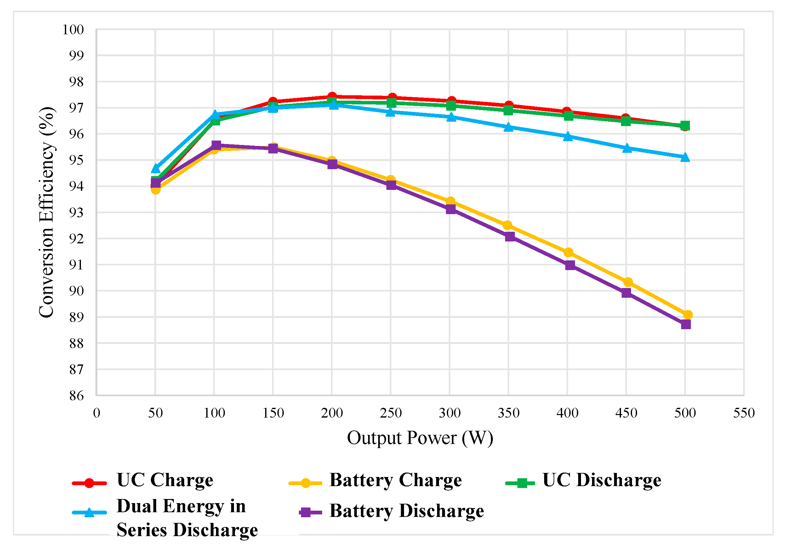
:A patented bidirectional power converter was studied as an interface to connect the DC-bus of driving inverter, battery energy storage (BES), and ultracapacitor (UC) to solve the problem that the driving motor damages the battery life during acceleration and deceleration in electric vehicles (EVs). The proposed concept was to adopt a multiport switch to control the power flow and achieve the different operating mode transitions for the better utilization of energy. In addition, in order to improve the conversion efficiency, the proposed converter used a coupled inductor and interleaved-pulse-width-modulation (IPWM) control to achieve a high voltage conversion ratio (i.e., bidirectional high step-up/down conversion characteristics). This study discussed the steady-state operation and characteristic analysis of the proposed converter. Finally, a 500 W power converter prototype with specifications of 72 V DC-bus, 24 V BES, and 48 V UC was built, and the feasibility was verified by simulation and experiment results. The highest efficiency points of the realized prototype were 97.4%, 95.5%, 97.2%, 97.1%, and 95.3% for the UC charge, battery charge, UC discharge, the dual-energy in series discharge, and battery discharge modes, respectively.

1. Introduction
Electric vehicle (EV) technologies are currently being developed to lessen environmental impact and overcome shortages of fossil fuel [1,2,3,4,5,6,7,8,9,10]. The typical power configuration of pure electric vehicle (EV) contains four major parts: the battery energy storage (BES), the power converter, the driving inverter of motor, and the energy management system (EMS) [6,8,10]. Among them, BES is the most critical component, which can directly affect the life and endurance of the EV, driving efficiency, and system performance. In general, the power will be drawn rapidly from the BES during the vehicle acceleration, subsequently causing BES output current and temperature to rise quickly. Moreover, the driving inverter is prone to generate less stable pulse currents for the BES during deceleration [9]. Such long-term use not only causes damage to the external body of the battery but also excessively charges and discharges the BES, which eventually will shorten the lifespan of the BES, specifically in high power applications. Although it is feasible to size up the BES for high power demands, the high price of the overall system still remains an issue. Possible solutions may be to select an ultracapacitor (UC), to assist BES, forming a “hybrid energy” system as shown in Figure 1 for EVs [11,12].
UC has high-power density, long cycle life, quick dynamic response, but low-energy-density, which are opposite toward BES. Hence, it should exploit the complementary properties of both the UC and the BES [12]. Several conventional schemes integrating both the BES and UC are shown in Figure 1. These schemes have all been designed to control power flows, supply specific voltages to loads, and to reduce design cost, mass, and power consumptions [12,13,14,15].
Figure 1a shows the most basic parallel scheme of the BES and UC, with the latter serving as the low-pass filter [16]. Although simple, the energy stored in the UC is not utilized effectively due to the absence of power converters. The slightly more robust Figure 1b shows that a power converter is added in between the BES and UC [17,18,19,20]. In this scheme, the BES is connected directly to the DC-bus instead of the UC. The power output of the UC is controlled by the power converter, and this enables the UC to operate over a wider voltage range than in Figure 1a. Due to this, the power rating of the converter has to be sufficiently large to handle high surges of power demands from the UC. The purpose of the power converter is also to maintain a constant voltage value on the DC-bus during the operation of the motor. The drawback of this scheme is that the BES is exposed to large fluctuations of high charging and discharging current, resulting in its reduced lifetime. Figure 1c is similar to Figure 1b except that the positions of the BES and UC have been swapped [21]. Due to this, the BES is no longer exposed to the large current fluctuations. The power output from the BES is now controlled by the power converter. The main disadvantage of this scheme is that the DC-bus voltage is exposed to large voltages as it is directly connected to the UC. As a result, the power converter is exposed to a high risk of suffering adverse losses, especially in harsh driving conditions.
All the schemes in Figure 1a–c clearly demonstrate that it is insufficient to use only one or no power converter. Hence, cascaded schemes using two power converters, as shown in Figure 1d,e, have also been considered before [22,23]. In these two schemes, two converters decouple the BES and UC from the DC-bus. The circuit, in Figure 1d, is also known as the “type-I scheme” where an extra power converter is added in between the UC and the DC-bus. The converter that is located in between the BES and UC is rated according to the power rating of the BES. This scheme creates more losses for the higher rated converter that is located in between the UC and the DC-bus due to the fluctuations of the UC output voltage. In order to overcome this problem, the positions of the BES and UC are swapped, as shown in Figure 1e (type-II scheme). However, it is difficult to balance the BES cell due to it now being located at the higher voltage terminal. Although both the type-I and type-II schemes are more robust than all the previous designs that use only one or no power converter, the power losses and design costs of the schemes are increased substantially owing to the multi-stage energy conversion processes in the vehicular power train. Besides that, only one power converter is connected to the DC-bus in both of these schemes. An outage in one of the power converters will lead to the loss of the power-control function. An alternative is to employ the scheme in Figure 1f, where the power converters are connected in parallel and directly to the DC-bus [13,24,25,26,27,28]. In this scheme, the power converters have the same output voltage, and the power flow of both the energy sources (BES and UC) are not affected by the output of the other converter. Consequently, this scheme can operate in various modes [28]. But, the fully power-rated converters are needed, and the cost of this scheme is higher than all the aforementioned schemes.
In order to reduce the overall system cost, a multi-input power converter scheme is studied, as shown in Figure 2, into the EV system [29,30,31,32,33].
Multi-input power converters are potential solutions when multiple energy sources with different voltage levels (battery voltage ≠ UC voltage ≠ DC-bus voltage) and/or power capabilities are to be combined and yet maintain a regulated output load voltage across them.
Using multi-input power converters, it is possible to apply a different power control command for each input source. In order to reduce the cost and weight and enhance the overall performance of the hybrid energy storage system, the multi-input power converter scheme was chosen in this paper and further investigated.
In [29], a multi-input power converter topology has been proposed to combine various input energy sources in parallel by using a single-pole triple-throw switch. The major limitations of parallel-connected source topologies are: input source voltage should be asymmetric, and only one input source can supply power to the load at a time to avoid the power coupling effect.
In [30], a single-inductor unidirectional multi-input power converter has been presented, which can operate in buck, boost, or buck-boost modes. To realize the bidirectional power flow mode, all the diodes must be replaced by unidirectional switches, which increase the number of switches.
In [31], a DC-bus interfacing three-port converter with a simple topology and no electrical isolation has been proposed, but it cannot cope with a wide operating voltage ratio; energy storage devices connected to different ports must have a similar operating voltage, and this constricts the application.
In [32], a modular multi-input power converter has been presented to integrate the basic buck-boost circuit and a shared DC-bus. It is a very simple approach to integrate multiple converters into a single unit. However, it has limited static voltage gains, resulting in a narrow voltage range and a low voltage difference between the high- and low-side ports. Besides, since only a few circuit elements are shared among multiple converters, the benefits of the integration are limited.
In [33], a two-phase multi-input converter with a high voltage conversion ratio has been proposed as an interface between dual-energy storage sources. Due to the intrinsic automatic current balance characteristic, the currents of two energy sources are theoretically identical; it indicates that the high power capability of UC cannot be utilized, and the applications of the proposed converter would be limited.
By conducting a research literature review of [29,30,31,32,33,34,35,36], in this paper, a bidirectional power converter integrated BES/UC dual-energy storage was proposed, which had the capability to perform forward power transmission and reverse energy recovery.
First, the proposed converter used a multiport switch to change the different operating modes and to improve the energy utilization of UC and increase battery life.
Second, it was also integrated with interleaved-pulse-width-modulation (IPWM) control to increase power density and reduce bidirectional current ripples, which makes power delivery more reliable.
Third, the proposed converter also used a coupled inductor technique instead of a general single-winding inductor to achieve high voltage conversion ratio and high power density for bidirectional power conversion.
Finally, the steady-state operation and characteristic analysis of the proposed converter were described, validated using simulation and experimentation of a 500 W power converter prototype with specifications of 72 V DC-bus, 24 V BES, and 48 V UC.
The summarized main features of the proposed converter were its ability to:
- (1)
- interface more than two energy sources of different voltage levels,
- (2)
- control power flow between the DC-bus and the two low-voltage energy sources,
- (3)
- control power flow from either the UC or BES or both,
- (4)
- enhance static voltage gain and reduce switch voltage stress, and
- (5)
- possess a reasonable duty cycle and produce a wide voltage difference between its high- and low-side ports.
2. Converter Operating Principles
Figure 3 shows the architecture of the proposed converter integrated with dual-energy storage. The power devices (S1~S4) are the multiport switch used to control the power flow between the battery/UC dual-energy and DC-bus. To achieve the high conversion efficiency, the design concept for the converter are based on multi-phase operation and switch stress reduction as (1) the power devices (Q1~Q4) are designed to use IPWM control to reduce current stress and ripple on the switch, (2) two-phase coupled inductors T1 and T2 are integrated into the bidirectional power converter with high turns ratio to reduce the undesirable duty ratio and conduction loss of metal-oxide-semiconductor field-effect transistors (MOSFETs).
2.1. Multiport Switch
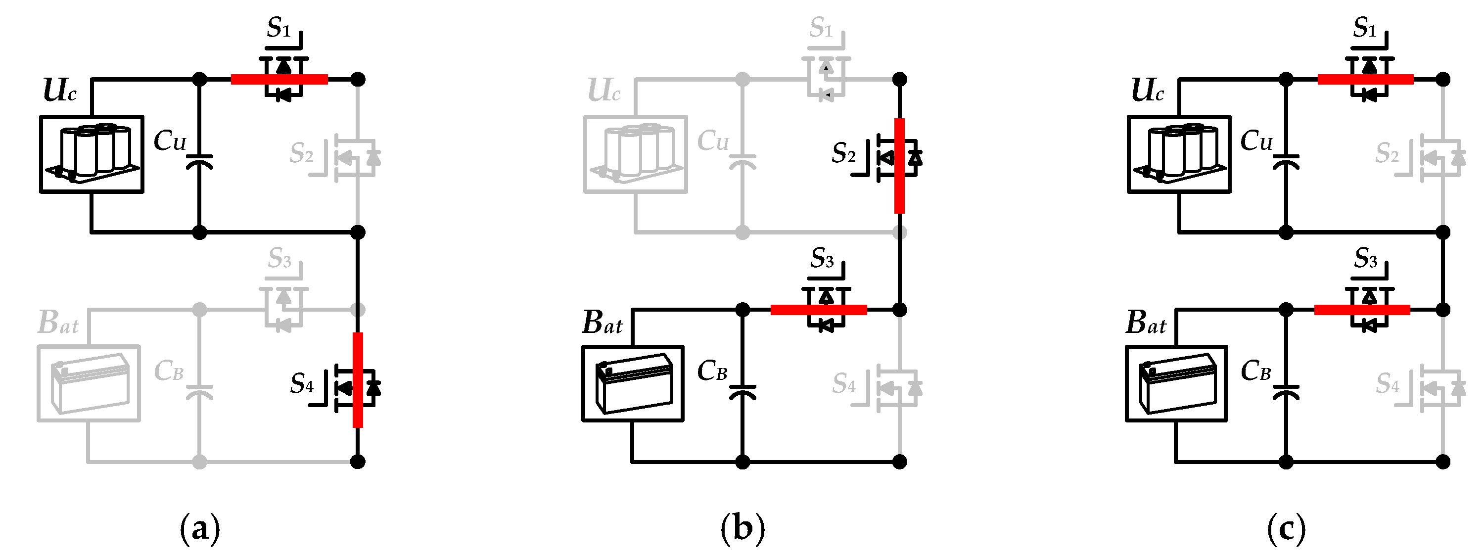
Figure 4 shows the equivalent circuits of the multiport switch of the proposed converter under different operating modes. For the converter operating in the UC charge or discharge mode, the multiport switches S1, S4 are turned on, and S2, S3 are turned off. The equivalent circuit of this condition is shown in Figure 4a. It is shown that the bidirectional energy delivery between the UC and the DC-bus can be achieved. For the converter operating under the battery charge mode or discharge mode, the multiport switches S2, S3 are turned on, and S1, S4 are turned off. Under this condition, the corresponding equivalent circuit is shown in Figure 4b. The figure shows that the bidirectional energy delivery between the battery and the DC-bus can be achieved. For the converter operating under the dual-energy in series discharge mode, the multiport switches S1, S3 are turned on, and S2, S4 are turned off. The battery/UC dual-energy delivers the energy to DC-bus, and its equivalent circuit is shown in Figure 4c.
2.2. Operating Principle of the Proposed Converter
Figure 5 shows the equivalent circuits of the different states for the proposed converter, where VH represents the high-side voltage for the DC-bus, and VL represents low-side voltage for UC, battery, or battery/UC dual-energy in series modes.
The assumptions are made in analyzing the proposed converter:
- (1)
- the converter operates in continuous conduction mode (CCM);
- (2)
- characteristic of the two-phase coupled inductors T1 and T2 are the same, i.e., Lm1 = Lm2, im1 = im2 and n = N2/N1 = N4/N3;
- (3)
- all voltages and currents in the circuits are periodic in steady-state condition; for simplicity, it is assumed that all the components in Figure 3 are idealized.
State 1. The equivalent circuit of this state is shown in Figure 5a. The power switches Q2 and Q4 are turned on, and Q1 and Q3 are turned off. During this state, the high-side voltage VH stores energy to the magnetizing inductance Lm1 and Lm2, and then the magnetizing currents im1, im2 increase linearly. The circuit equations are expressed as follows,
State2. The equivalent circuit of this state is shown in Figure 5b. The power switches Q2 and Q3 are turned on, and Q1 and Q4 are turned off. At this time, the high-side voltage VH continues to store energy to the magnetizing inductance Lm1, and the magnetizing current im1 increases linearly. The energy stored in the magnetizing inductor Lm2 is now released to the low-side energy device, and the magnetizing current im2 decreases linearly. The circuit equations are expressed as follows,
State 3. The equivalent circuit of this state is shown in Figure 5c. The power switches Q1 and Q4 are turned on, and Q2 and Q3 are turned off. At this time, the energy stored in the magnetizing inductor Lm1 is now released to the low-side energy storage, and the magnetizing current im1 decreases linearly. The voltage across vN1 of the magnetizing inductor Lm1 is negative of the low-side voltage VL. The magnetizing inductor Lm2 draws the energy from the high-side voltage VH, and the magnetizing current im2 increases linearly. The circuit equations are expressed as follows,
State 4. The equivalent circuit of this state is shown in Figure 5d. The power switches Q1 and Q3 are turned on, and Q2 and Q4 are turned off. At this time, the energy stored in the magnetizing inductor Lm1 and Lm2 is now released to the low-side energy storage, and the magnetizing currents im1 and im2 decrease linearly. The voltage across vN1 and vN3 of the magnetizing inductor Lm1 and Lm2 is negative of the low-side voltage VL. The circuit equations are expressed as follows,
Considering the different duty ratio conditions in the charge mode and discharge mode, the operating state flow of each condition during a switching period is summarized as follows.
Charge Mode (Dc < 0.5)
| State 2 → State 4 → State 3 → State 4 |
Charge Mode (Dc = 0.5)
| State 2 → State 3 |
Charge Mode (Dc > 0.5)
| State 2 → State 1 → State 3 → State 1 |
Discharge Mode (Dd < 0.5)
| State 3 → State 1 → State 2 → State 1 |
Discharge Mode (Dd = 0.5)
| State 3 → State 2 |
Discharge Mode (Dd > 0.5)
| State 3 → State 4 → State 2 → State 4 |
As mentioned above, Dc is the duty ratio of switch Q2 and Q4 for the charge mode, and Dd is the duty ratio of switch Q1 and Q3 for the discharge mode.
When the proposed converter operates with the duty ratio of 0.5 in the charge or discharge mode (i.e., Dc = Dd = 0.5), the only two operating states of the proposed converter are produced.
When the proposed converter operates in the charge mode with duty ratio Dc > 0.5, the operation state in a switching period is the same as the discharge mode with Dd < 0.5, and only the reverse current direction is considered.
Similarly, when the proposed converter operates in the discharge mode with the duty ratio Dd > 0.5, the operation state in the switching period is the same as the charge mode with Dc < 0.5, and only the reverse current direction is considered. Figure 6 shows the key waveforms of the proposed converter in the charge mode with Dc < 0.5, and in the discharge mode with Dd < 0.5, respectively.
The time intervals of Figure 6 are described as
Charge Mode (Dc < 0.5)
[t0 < t ≤ t1]: state 2; [t1 < t ≤ t2]: state 4; [t2 < t ≤ t3]: state 3; [t3 < t ≤ t4]: state 4.
Discharge Mode (Dd < 0.5)
[t0 < t ≤ t1]: state 3; [t1 < t ≤ t2]: state 1; [t2 < t ≤ t3]: state 2; [t3 < t ≤ t4]: state 1.
3. Converter Steady-State Analyses
3.1. Static Voltage Conversion Ratio Analysis
Charge Mode (UC Charge; Battery Charge)
During steady-state operation and according to the volt-second balance principle of the magnetizing inductance operating in the charge mode, the static voltage conversion ratio Mc can be derived as from (22)–(25).
The voltage relationship between primary and secondary sides of the coupled inductor is shown as follows
substituting (22) into (1), it can be rewritten as follows
By combining (23) and (12), the average voltage of the primary side for the coupled inductor during a switching period can be expressed as follows
The static voltage conversion ratio of the proposed converter in the charge mode can be derived as follows
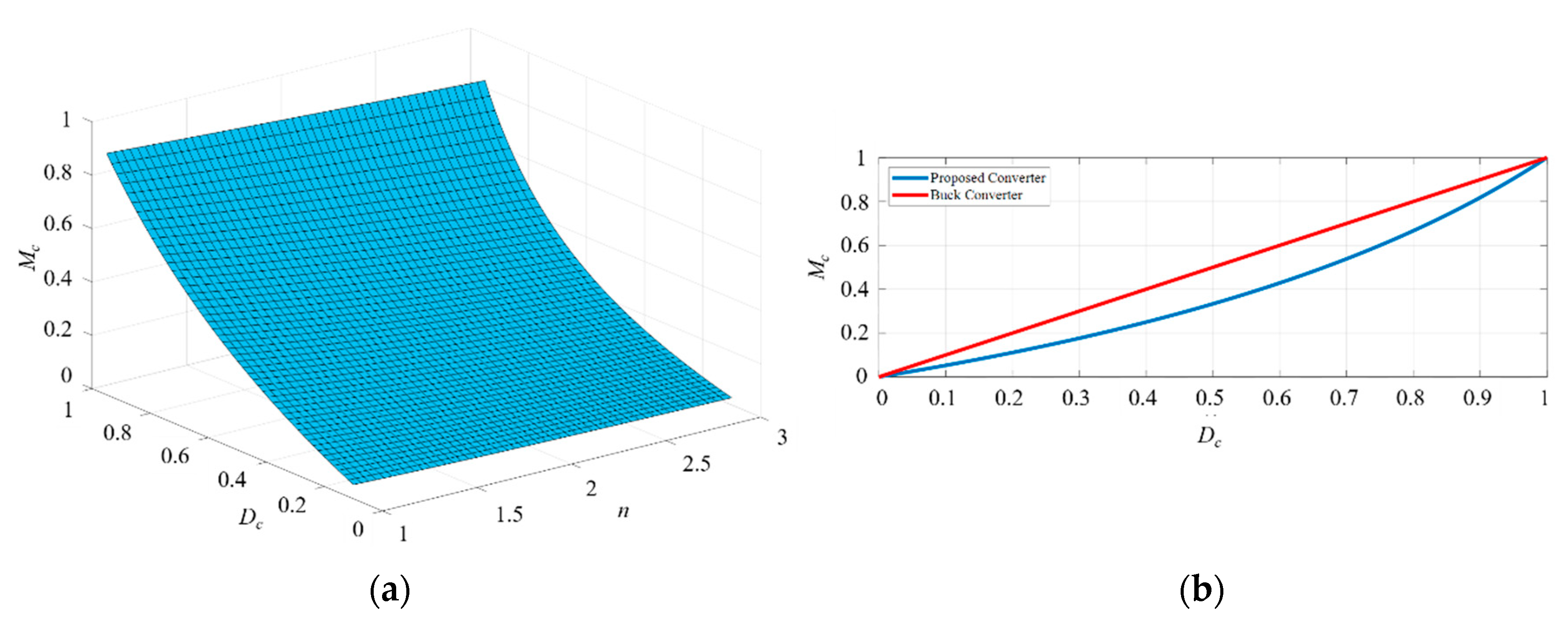
Figure 7a shows the relationship between the coupled inductance with different turns ratio and the static voltage conversion ratio Mc of the proposed converter in the charge mode.
For simplicity, assuming that the turns ratio of the coupling inductance is n = 1, the relationship between Mc and Dc is shown in Figure 7b.
It can be seen that the static voltage conversion ratio of the proposed converter in the charge mode has a better performance, compared with the conventional buck converter.
Discharge Mode (UC Discharge; Battery Discharge; Dual-Energy in Series Discharge)
The static voltage conversion ratio Md in the discharge mode can be derived from the average voltage of the magnetizing inductance. According to (23) and (12), and considering the duty ratio Dd of the switch Q1 and Q3, the average voltage of the primary side for the coupled inductor during a switching period can be expressed as follows
The static voltage conversion ratio of the converter in the discharge mode can be derived as follows
Figure 8a shows the relationship between the coupled inductance with different turns ratios and the static voltage conversion ratio Md of the proposed converter in the discharge mode. For simplicity, assuming that the turns ratio of the coupling inductance is n = 1, the relationship between Md and Dd is shown in Figure 8b. It can be seen that the static voltage conversion ratio of the proposed converter in the discharge mode has a better performance, compared with the conventional boost converter.
3.2. Boundary Condition Analysis
Charge Mode (UC Charge; Battery Charge)
According to the ampere-second balance principle for the filter capacitor CL on the low-voltage side, it means that the average current of the filter capacitor should be zero in steady-state, and the sum of the averaged currents IT1 and IT2 are equal to the low-side current IL,BCM (i.e., UC current or battery current), as described below
In (28), RL,BCM represents the low-side equivalent resistance under boundary-conduction-mode (BCM) condition.
Considering the low-side voltage VL is constant, the peak value of the magnetizing current imc1,pk at BCM in the charge mode can be expressed as
where Ts is the switching period.
Substituting (29), (30), and (31) into (28), the boundary magnetizing inductance Lmc,BCM in the charge mode can be derived as follows
The boundary time constant τc,BCM of the proposed converter in the charge mode can be derived as (33), and the corresponding relationship curve is depicted as shown in Figure 9.
Discharge Mode (UC Discharge; Battery Discharge; Dual-Energy in Series Discharge)
According to the ampere-second balance principle of the filter capacitor CH on the high-voltage side, it can be shown that the average current on the filter capacitor is zero in steady-state, and the sum of the averaged currents IN2 and IN4 are equal to the high-side current IH,BCM (i.e., DC-bus current) as described below
where RH,BCM represents the high-side equivalent resistance under BCM.
Considering the high-side voltage VH is constant, the peak value of the magnetizing current imd1,pk at BCM in the discharge mode can be expressed as follows
Substituting (35), (36) into (34) and simplifying it, the boundary magnetizing inductance in the discharge mode can be derived as follows
The boundary time constant τd,BCM of the converter in the discharge mode can be derived as (38), and the corresponding relationship curve is depicted as shown in Figure 10.
3.3. Voltage and Current Stresses Analyses of Power Devices
3.3.1. Voltage Stress Derivations
The power switching device is the main design considerations when implementing the power converter. The voltage and current stresses of the power device for the converter circuit are analyzed, and then the appropriate components are selected as below.
The multiport switches S1~S4 are used as the pre-stage for the discharge mode or post-stage for the charge mode. The voltage stress of the multiport switches S1 and S2 is equal to the UC voltage VU, and the voltage stress of S3 and S4 is equal to the battery voltage VB, as follows
The voltage stress of the power switches Q1 to Q4 for the converter can be expressed as follows
3.3.2. Current Stress Derivations
The root mean square (RMS) current of the magnetizing inductances Lm1 and Lm2 are derived based on the operating state of the proposed converter, as follows
where Im1 and Im2 are the DC value of the magnetizing current im1 and im2, respectively; Δim1 and Δim2 are the magnetizing ripple currents, as follows
The RMS current of the power switches Q1~Q4 of the proposed converter in the charge mode can be derived as follows
The RMS current of the filter capacitors CL and CH of the proposed converter in the charge mode can be derived as follows
where
4. Simulated and Experimented Results
The realized converter prototype is shown in Figure 11, and Table 1 shows the electrical specifications and the circuit parameters of the realized power converter. For the convenience of the experiments, in the charge mode, the power supply (ITECH IT6726G) was used as the DC-bus on the high-voltage side, and the electronic load (ITECH IT8814B) was used as the UC or the battery on the low-voltage side. Conversely, in the discharge mode, the power supply was used as the UC, the battery, or the dual-energy storage in series.
UC Charge Mode
Figure 12 and Figure 13 show the waveforms of the gate signals of Q2 and Q4, the primary-side currents of the coupled inductor (iT1, iT2), the secondary-side currents of the coupled inductor (iN2, iN4), and the low-side voltage VU in the UC charge mode with full load condition, respectively. In this mode, the UC voltage was about 48 V, the duty ratio of the switches Q2 and Q4 was set to 80% (i.e., Dc = 0.8), the DC values of the primary currents (iT1, iT2) and secondary currents (iN2, iN4) of the coupled inductance were about 5.2 A and 3.5 A, respectively.
Figure 14 shows the waveforms of the steady-state switching voltages across the power devices in the UC charge mode. The results showed that the steady-state switching voltages across the lower-leg MOSFETs Q1 and Q3 were about 60 V, and the steady-state switching voltages across the upper-leg MOSFETs Q2 and Q4 were about 120 V. It could be seen that in Figure 14, the simulation and the experimental results were consistent and corresponded to (41) and (42).
Battery Charge Mode
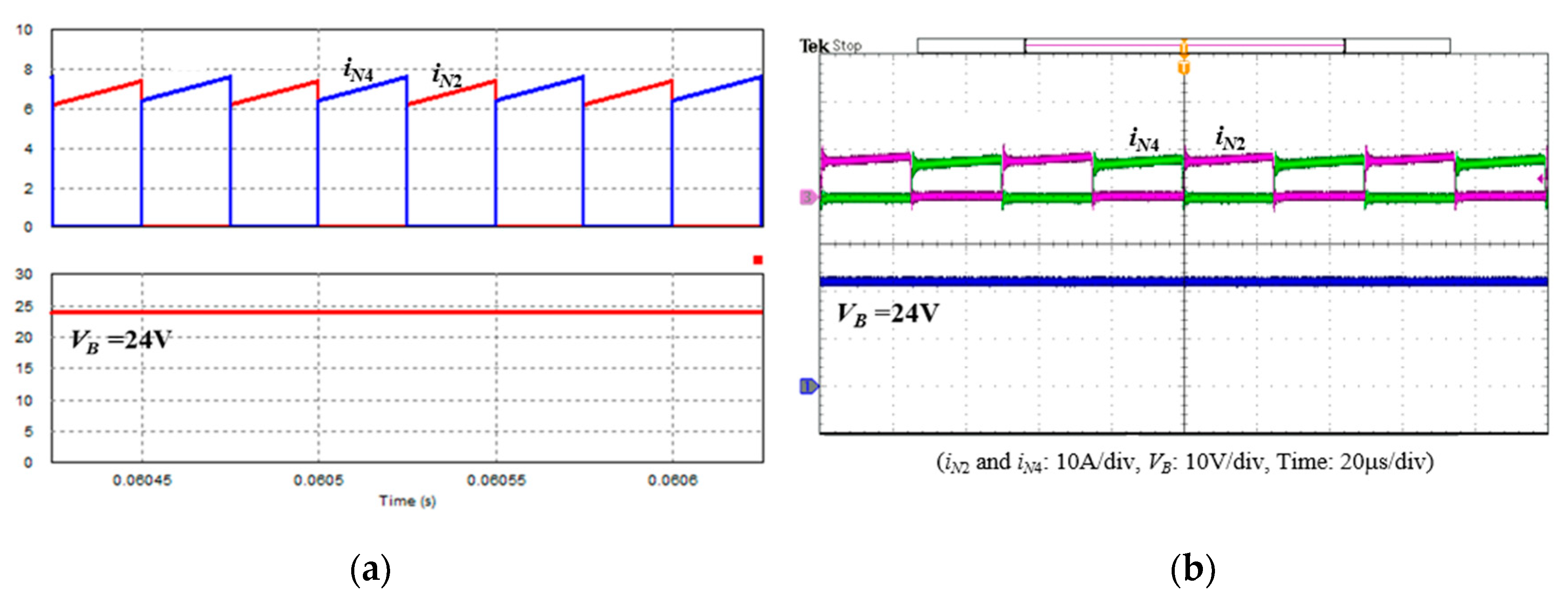
Figure 15 and Figure 16 show the waveforms of the gate signals of Q2 and Q4, the primary-side currents of the coupled inductor (iT1, iT2), the secondary-side currents of the coupled inductor (iN2, iN4), and the low-side voltage VU in the battery charge mode with full load condition, respectively.
In this mode, the battery voltage was about 24 V, the duty ratio of the switches Q2 and Q4 was set to 50% (i.e., Dc = 0.5), and the DC values of the primary currents (iT1, iT2) and secondary currents (iN2, iN4) of the coupled inductance were about 10.4 A and 3.5 A, respectively. It could be seen that in Figure 15 and Figure 16, the simulation and the experimental results were consistent.
Figure 17 shows the waveforms of the steady-state switching voltages across the power devices in the battery charge mode. The results showed that the steady-state switching voltages across the lower-leg MOSFETs Q1 and Q3 were about 48 V, and the steady-state switching voltages across the upper-leg MOSFETs Q2 and Q4 were about 96 V. It could be seen that in Figure 17, the simulation and the experimental results were consistent and corresponded to (41) and (42).
UC Discharge Mode
Figure 18 and Figure 19 show the waveforms of the gate signals of Q2 and Q4, the primary-side currents of the coupled inductor (iT1, iT2), the secondary-side currents of the coupled inductor (iN2, iN4), and the high-side voltage VH in the UC discharge mode with full load condition, respectively.
In this mode, the DC-bus voltage was about 72 V, the duty ratio of the switches Q1 and Q3 was set to 20% (i.e., Dd = 0.2), and the DC values of the primary currents (iT1, iT2) and secondary currents (iN2, iN4) of the coupled inductance were about 5.2 A and 3.5 A, respectively. It could be seen that in Figure 18 and Figure 19, the simulation and the experimental results were consistent.
Figure 20 shows the waveforms of the steady-state switching voltages across the power devices in the UC discharge mode. The results showed that the steady-state switching voltages across the lower-leg MOSFETs Q1 and Q3 were about 60 V, and the steady-state switching voltages across the upper-leg MOSFETs Q2 and Q4 were about 120 V. It could be seen that in Figure 20, the simulation and the experimental results were consistent and corresponded to (41) and (42).
Dual-Energy in Series Discharge Mode
Figure 21 and Figure 22 show the waveforms of the gate signals of Q2 and Q4, the primary-side currents of the coupled inductor (iT1, iT2), the secondary-side currents of the coupled inductor (iN2, iN4), and the high-side voltage VH in the dual-energy discharge mode with full load condition, respectively.
In this mode, the DC-bus voltage was about 72 V, the low-side voltage VL was 44 V, the duty ratio of the switches Q1 and Q3 was set to 25% (i.e., Dd = 0.25), and the DC values of the primary currents (iT1, iT2) and secondary currents (iN2, iN4) of the coupled inductance were about 5.8 A and 3.5 A, respectively. It could be seen that in Figure 21 and Figure 22, the simulation and the experimental results were consistent.
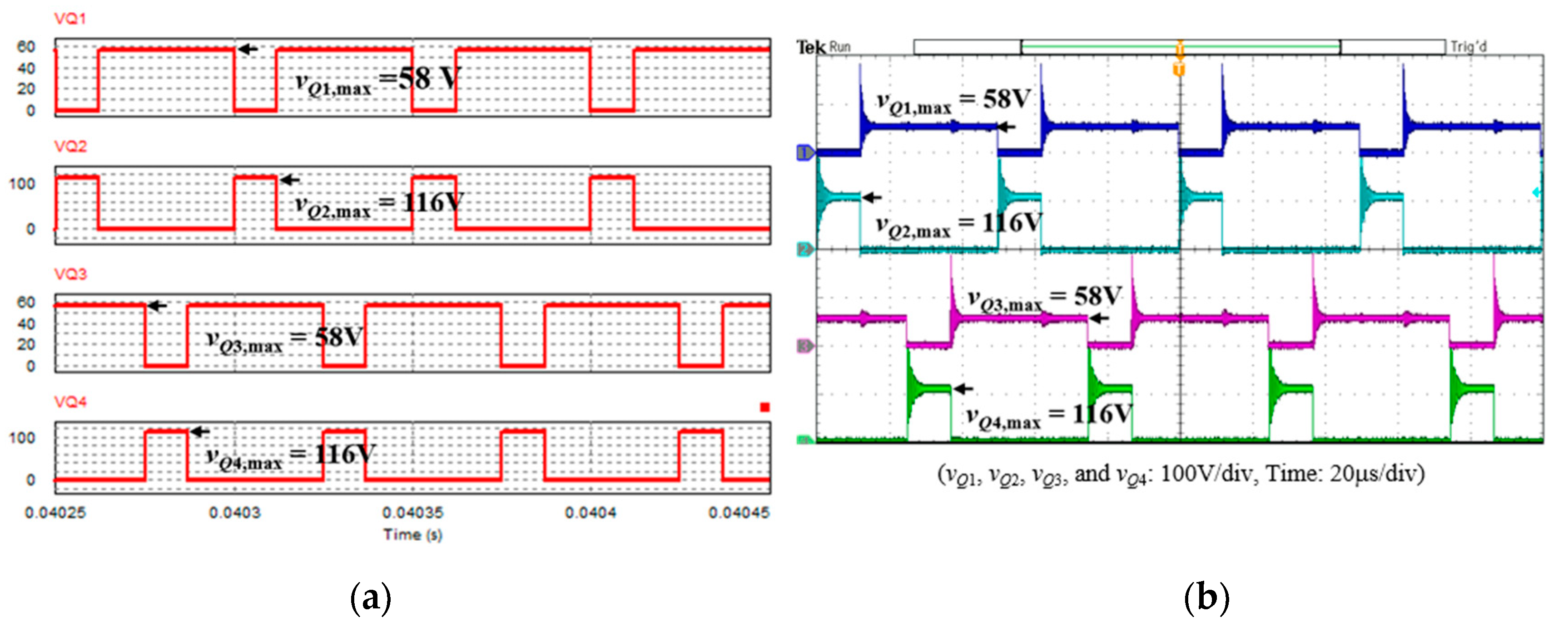
Figure 23 shows the waveforms of the steady-state switching voltages across the power devices in the dual-energy in series discharge mode. The results showed that the steady-state switching voltages across the lower-leg MOSFETs Q1 and Q3 were about 58 V, and the steady-state switching voltages across the upper-leg MOSFETs Q2 and Q4 were about 116 V. It could be seen that in Figure 23, the simulation and the experimental results were consistent and corresponded to (41) and (42).
Efficiency Measurement
The system used two power analyzers (YOKOGAWA WT310) connected to the input and output of the realized converter prototype. As could be seen in Figure 24, in the UC charge mode, the highest efficiency point was 97.4%; in the battery charge mode, the highest efficiency point was 95.5%; in the UC discharge mode, the highest efficiency point was 97.2%; in the dual-energy in series discharge mode, the highest efficiency point was 97.1%; in the battery discharge mode, the highest efficiency point was 95.3%.
5. Conclusions
This study proposed a patented bidirectional power converter that used dual-energy storage as input sources and incorporated a coupled inductor to obtain a higher voltage conversion ratio. The converter control used IPWM control to achieve low current ripple, dissipate low side current stress, and reduce the conduction loss of the power MOSFET. Moreover, the proposed bidirectional power converter in this study also discussed the steady-state operation in the charge mode and discharge mode, respectively. The voltage conversion ratio, boundary conditions, and voltage and current stress of each power component of the converter were analyzed. Finally, this study implemented a converter prototype with a 500 W power rating for verification. The simulation results and the experimental results were consistent; the highest efficiency points of the realized prototype were 97.4%, 95.5%, 97.2%, 97.1%, and 95.3% for the UC charge mode, battery charge mode, UC discharge mode, the dual-energy in series discharge mode, and battery discharge mode, respectively. In summary, this paper demonstrated that the proposed bidirectional power converter could be potentially applied to produce hybrid power architecture (has been patented [37]).
Author Contributions
C.-M.L. substantially contributed to the examination and interpretation of the results, development of the overall system, and review and proofreading of the manuscript. J.T. and Y.L. substantially contributed to the review and proofreading of the manuscript. Y.-C.L. substantially contributed to literature search, control strategy design, and production and analysis of the results. All authors have read and agreed to the published version of the manuscript.
Funding
This work was supported in part by the Ministry of Science and Technology (MOST), Taiwan, R.O.C., under grant MOST-107-2221-E-005-079-MY3, MOST-107-2221-E-005-080-MY2, MOST-108-2218-E-005-021, and MOST-108-2638-E-005-001-MY2.
Acknowledgments
The authors would like to express their appreciation to the Chih-Yu Yang (guided by Prof. Ching-Ming Lai) for the experimental bench setup.
Conflicts of Interest
The authors declare no conflict of interest.
Nomenclature
| T1, T2 | Two-phase coupled inductors |
| Lm1, Lm2 | Magnetizing inductors of the two-phase coupled inductors |
| Lmc,BCM | Boundary magnetizing inductance in the charge mode |
| Lmd,BCM | Boundary magnetizing inductance in the discharge mode |
| n | Turns ratio of the two-phase coupled inductors (n = N2/N1 = N4/N3) |
| N1 | Primary winding of T1 |
| N2 | Secondary winding of T1 |
| N3 | Primary winding of T2 |
| N4 | Secondary winding of T2 |
| k | Coupling coefficient |
| CU | Input capacitor paralleled with UC |
| CB | Input capacitor paralleled with BES |
| S1~S4 | Power devices of the multiport switch |
| Q1~Q4 | Power devices of the two-phase bidirectional power converter |
| VH | High-side voltage for the DC-bus |
| VL | Low-side voltage for UC, BES, or BES/UC dual-energy in series |
| VU | UC voltage |
| VB | BES voltage |
| iBus | DC-bus current |
| iUc | UC current |
| iBat | BES current |
| iH | High voltage side current |
| iL | Low voltage side current |
| IL,BCM | Low voltage side current under BCM condition |
| IH,BCM | High voltage side current under BCM condition |
| Im1,rms, Im2,rms | RMS value of the magnetizing currents of the coupled inductors |
| IT1,rms, IT2,rms | RMS value of the primary-side currents of the coupled inductors |
| vN1 | Voltage of the winding N1 of the T1 |
| vN2 | Voltage of the winding N2 of the T1 |
| vN3 | Voltage of the winding N3 of the T2 |
| vN4 | Voltage of the winding N4 of the T2 |
| VS1,max~VS4,max | Switch voltage stress of the multiport switch |
| VQ1,max~VQ4,max | Switch voltage stress of the two-phase bidirectional power converter |
| iT1, iT2 | The primary-side currents of the two-phase coupled inductors |
| iT | The sum of the primary-side currents iT1 and iT2 |
| iN2, iN4 | The secondary-side currents of the two-phase coupled inductors |
| im1, im2 | Magnetizing inductor currents of the coupled inductors T1 and T2 |
| Im1, Im2 | DC value of the magnetizing currents |
| imc,pk | peak value of the magnetizing inductor current under BCM in the charge mode |
| imd,pk | peak value of the magnetizing inductor current under BCM in the discharge mode |
| Δim1, Δim2 | Magnetizing ripple currents |
| IQ1,rms~IQ4,rms | RMS current of the power switches Q1~Q4 |
| ICH,rms~ICL,rms | RMS current of the filter capacitors CL and CH |
| Dc, Dd | Duty ratio of charge mode and discharge mode |
| Ts | Switching period |
| τc,BCM | Boundary time constant in the charge mode |
| τd,BCM | Boundary time constant in the discharge mode |
| RL,BCM | Low-side equivalent resistance under BCM condition |
| RH,BCM | High-side equivalent resistance under BCM condition |
| Mc | Static voltage conversion ratio in the charge mode |
| Md | Static voltage conversion ratio in the discharge mode |
References
- Lai, J.S.; Nelson, D.J. Energy management power converters in hybrid electric and fuel cell vehicles. Proc. IEEE 2007, 95, 766–777. [Google Scholar] [CrossRef]
- Bauman, J.; Kazerani, M. A comparative study of fuel-cell-battery, fuel-cell-ultracapacitor, and fuel-cell-battery-ultracapacitor vehicles. IEEE Trans. Veh. Technol. 2008, 57, 760–769. [Google Scholar] [CrossRef]
- Khaligh, A.; Li, Z. Battery ultracapacitor fuel cell and hybrid energy storage systems for electric hybrid electric fuel cell and plug-in hybrid electric vehicles: State of the art. IEEE Trans. Veh. Technol. 2010, 59, 2806–2814. [Google Scholar] [CrossRef]
- Chan, C.C.; Bouscayrol, A.; Chen, K. Electric, hybrid, and fuel-cell vehicles: Architectures and modeling. IEEE Trans. Veh. Technol. 2010, 59, 589–598. [Google Scholar] [CrossRef]
- Rajashekara, K. Present status and future trends in electric vehicle propulsion technologies. IEEE J. Emerg. Sel. Top. Power Electron. 2013, 1, 3–10. [Google Scholar] [CrossRef]
- Zhang, Y.; Meng, D.; Zhou, M.; Li, S. Energy management of an electric city bus with battery/ultra-capacitor HESS. In Proceedings of the 2016 IEEE Vehicle Power and Propulsion Conference (VPPC), Hangzhou, China, 17–20 October 2016. [Google Scholar]
- Cheng, Y.H.; Lai, C.M. Control strategy optimization for parallel hybrid electric vehicles using memetic algorithm. Energies 2017, 10, 305. [Google Scholar] [CrossRef] [Green Version]
- Cheng, L.; Acuna, P.; Aguilera, R.P.; Jiang, J.; Flecther, J.; Baier, C. Model predictive control for energy management of a hybrid energy storage system in light rail vehicles. In Proceedings of the 2017 11th IEEE International Conference on Compatibility, Power Electronics and Power Engineering (CPE-POWERENG), Cadiz, Spain, 4–6 April 2017; pp. 683–688. [Google Scholar]
- Un-Noor, F.; Padmanaban, S.; Mihet-Popa, L.; Mollah, M.N.; Hossain, E.A. Comprehensive study of key electric vehicle (EV) components, technologies, challenges, impacts, and future direction of development. Energies 2017, 10, 1217. [Google Scholar] [CrossRef] [Green Version]
- Serpi, A.; Porru, M. Modelling and design of real-time energy management systems for fuel cell/battery electric vehicles. Energies 2019, 12, 4260. [Google Scholar] [CrossRef] [Green Version]
- Schaltz, E.; Khaligh, A.; Rasmussen, P.O. Influence of battery/ultracapacitor energy-storage sizing on battery lifetime in a fuel cell hybrid electric vehicle. IEEE Trans. Veh. Technol. 2009, 58, 3882–3891. [Google Scholar] [CrossRef]
- Cao, J.; Emadi, A. A new battery/ultracapacitor hybrid energy storage system for electric, hybrid, and plug-in hybrid electric vehicles. IEEE Trans. Power Electron. 2012, 27, 122–132. [Google Scholar]
- Momayyezan, M.; Hredzak, B.; Agelidis, V.G. A new multiple converter topology for battery/ultracapacitor hybrid energy system. In Proceedings of the Annual Conference of the IEEE Industrial Electronics Society, Yokohama, Japan, 9–12 November 2015; pp. 464–468. [Google Scholar]
- Juned, S.; Mohammad, S.; Bhanabhagvanwala, D. Simulation analysis of battery/ultracapacitor hybrid energy storage system for electric vehicle. In Proceedings of the International Conference on Intelligent Sustainable Systems, Palladam, India, 21–22 February 2019. [Google Scholar]
- Chakraborty, S.; Vu, H.-N.; Hasan, M.M.; Tran, D.-D.; Baghdadi, M.E.; Hegazy, O. DC-DC converter topologies for electric vehicles, plug-in hybrid electric vehicles and fast charging stations: State of the art and future trends. Energies 2019, 12, 1569. [Google Scholar] [CrossRef] [Green Version]
- Ding, S.; Wei, B.; Hang, J.; Zhang, P.; Ding, M. A Multifunctional Interface Circuit for Battery-Ultracapacitor Hybrid Energy Storage System; NSW: Sydney, Australia, 2017. [Google Scholar]
- Ortúzar, M.; Moreno, J.; Dixon, J. Ultracapacitor-based auxiliary energy system for an electric vehicle: Implementation and evaluation. IEEE Trans. Ind. Electron. 2007, 54, 2147–2156. [Google Scholar] [CrossRef]
- Machado, F.; Antunes, C.H.; Dubois, M.R.; Trovao, J.P. Semi-active hybrid topology with three-level DC-DC converter for electric vehicle application. In Proceedings of the 2015 IEEE Vehicle Power and Propulsion Conference (VPPC), Montreal, QC, Canada, 19–22 October 2015; pp. 1–6. [Google Scholar]
- Shen, J.; Khaligh, A. A supervisory energy management control strategy in a battery/ultracapacitor hybrid energy storage system. IEEE Trans. Transp. Electrif. 2015, 1, 223–231. [Google Scholar] [CrossRef]
- Castaings, A.; Lhomme, W.; Trigui, R.; Bouscayrol, A. Practical control schemes of a battery/supercapacitor system for electric vehicle. IET Electr. Syst. Transp. 2016, 6, 20–26. [Google Scholar] [CrossRef]
- Kuperman, A.; Aharon, I.; Malki, S.; Kara, A. Design of a semiactive battery-ultracapacitor hybrid energy source. IEEE Trans. Power Electron. 2013, 28, 806–815. [Google Scholar] [CrossRef]
- Onar, O.; Khaligh, A. Dynamic modeling and control of a cascaded active battery/ultra-capacitor based vehicular power system. In Proceedings of the 2008 IEEE Vehicle Power and Propulsion Conference (VPPC), Harbin, China, 3–5 September 2008. [Google Scholar]
- Jing, W.; Lai, C.H.; Wong, S.H.W.; Wong, M.L.D. Battery-supercapacitor hybrid energy storage system in standalone DC microgrids: Areview. IET Renew. Power Gener. 2017, 11, 461–469. [Google Scholar] [CrossRef]
- Allegre, A.L.; Bouscayrol, A.; Trigui, R. Flexible real-time control of a hybrid energy storage system for electric vehicles. IET Electr. Syst. Transp. 2013, 3, 79–85. [Google Scholar] [CrossRef]
- Trovão, J.P.F.; Pereirinha, P.G. Control scheme for hybridised electric vehicles with an online power follower management strategy. IET Electr. Syst. Transp. 2015, 5, 12–23. [Google Scholar] [CrossRef]
- Trovao, J.P.; Silva, M.A.; Dubois, M.R. Coupled energy management algorithm for MESS in urban EV. IET Electr. Syst. Transp. 2017, 7, 125–134. [Google Scholar] [CrossRef]
- Livreri, P.; Castiglia, V.; Pellitteri, F.; Miceli, R. Design of a battery/ultracapacitor energy storage system for electric vehicle applications. In Proceedings of the IEEE International Forum on Research and Technologies for Society and Industry, Palermo, Italy, 10–13 September 2018; pp. 1–5. [Google Scholar]
- Lu, X.; Wang, H. Optimal sizing and energy management for cost-effective PEV hybrid energy storage systems. IEEE Trans. Ind. Inform. 2020, 16, 3407–3416. [Google Scholar] [CrossRef]
- Gummi, K.; Ferdowsi, M. Double-input DC–DC power electronic converters for electric-drive vehicles-Topology exploration and synthesis using a single-pole triple-throw switch. IEEE Trans. Ind. Electron. 2010, 57, 617–623. [Google Scholar] [CrossRef]
- Kumar, L.; Jain, S. Multiple-input DC/DC converter topology for hybrid energy system. IET Power Electron. 2013, 6, 1483–1501. [Google Scholar] [CrossRef]
- Lai, C.M.; Yang, M.J. A high-gain three-port power converter with fuel cell, battery sources and stacked output for hybrid electric vehicles and DC-microgrids. Energies 2016, 9, 180. [Google Scholar] [CrossRef] [Green Version]
- Hintz, A.; Prasanna, U.R.; Rajashekara, K. Novel modular multiple-input bidirectional DC-DC power converter (MIPC) for HEV/FCV application. IEEE Trans. Ind. Electron. 2015, 62, 3163–3172. [Google Scholar] [CrossRef]
- Lai, C.M.; Cheng, Y.H.; Hsieh, M.H.; Lin, Y.C. Development of a bidirectional DC/DC converter with dual-battery energy storage for hybrid electric vehicle system. IEEE Trans. Veh. Technol. 2018, 67, 1036–1052. [Google Scholar] [CrossRef]
- Hernándeza, J.C.; Ruiz-Rodriguezb, F.J.; Juradoc, F. Modelling and assessment of the combined technical impact of electric vehicles and photovoltaic generation in radial distribution systems. Energy 2017, 141, 316–332. [Google Scholar] [CrossRef]
- Hernándeza, J.C.; Sanchez-Sutila, F.; Muñoz-Rodríguezb, F.J. Design criteria for the optimal sizing of a hybrid energy storage system in PV household-prosumers to maximize self-consumption and self-sufficiency. Energy 2019, 186, 115827. [Google Scholar] [CrossRef]
- Gomez-Gonzaleza, M.; Hernandezb, J.C.; Veraa, D.; Juradoa, F. Optimal sizing and power schedule in PV household-prosumers for improving PV self-consumption and providing frequency containment reserve. Energy 2020, 191, 116554. [Google Scholar] [CrossRef]
- Lai, C.-M.; Yang, C.-Y.; Cheng, Y.-H. Power Supply System and Power Supply Method for Electric Vehicle. Taiwan Patent No. I642575, 1 December 2018. [Google Scholar]
Figure 1.
Several schemes of interfacing battery energy storage (BES) and ultracapacitor (UC) to the DC-bus in electric vehicle (EV) power train: (a) Directly parallel hybrid scheme; (b) UC/BES scheme; (c) BES/UC scheme; (d) type-I of cascaded scheme; (e) type-II of cascaded scheme; (f) multiple converter parallel scheme.

Figure 2.
Multi-input power converter interfacing BES and UC to the DC-bus in the EV power train.

Figure 3.
The proposed bidirectional power converter architecture.

Figure 4.
Equivalent circuits of the multiport switch under different operating modes. (a) UC charge mode or discharge mode. (b) Battery charge mode or discharge mode. (c) Battery/UC dual-energy in series discharge mode.
Figure 4.
Equivalent circuits of the multiport switch under different operating modes. (a) UC charge mode or discharge mode. (b) Battery charge mode or discharge mode. (c) Battery/UC dual-energy in series discharge mode.

Figure 5.
Equivalent circuits of the proposed converter. (a) State 1: Q2, Q4 on, and Q1, Q3 off. (b) State 2: Q2, Q3 on, and Q1, Q4 off. (c) State 3: Q1, Q4 on, and Q2, Q3 off. (d) State 4: Q1, Q3 on, and Q2, Q4 off. (The arrows in green indicate the charge mode, and the arrows in red indicate the discharge mode.).

Figure 6.
Key waveforms: (a) charge mode and Dc < 0.5; (b) discharge mode and Dd < 0.5.

Figure 7.
Converter characteristics in charge mode: (a) relationship diagram of Mc, Dc, and n; (b) relationship diagram of Mc and Dc (n = 1).
Figure 7.
Converter characteristics in charge mode: (a) relationship diagram of Mc, Dc, and n; (b) relationship diagram of Mc and Dc (n = 1).

Figure 8.
Converter characteristics in discharge mode: (a) relationship diagram of Md, Dd, and n; (b) relationship diagram of Md and Dd (n = 1).
Figure 8.
Converter characteristics in discharge mode: (a) relationship diagram of Md, Dd, and n; (b) relationship diagram of Md and Dd (n = 1).

Figure 9.
The curve of the boundary time constant τc,BCM in the charge mode.

Figure 10.
The curve of the boundary time constant τd,BCM in the discharge mode.

Figure 11.
Prototype circuit of the proposed converter.

Figure 12.
Waveforms of the switching gate signals and the primary-side currents of the coupled inductor in the UC recharging mode with Dc = 0.8: (a) simulated and (b) experimental.
Figure 12.
Waveforms of the switching gate signals and the primary-side currents of the coupled inductor in the UC recharging mode with Dc = 0.8: (a) simulated and (b) experimental.

Figure 13.
The waveform of the secondary-side currents of the coupled inductor and UC voltage in the UC charge mode with Dc = 0.8: (a) simulated and (b) experimental.
Figure 13.
The waveform of the secondary-side currents of the coupled inductor and UC voltage in the UC charge mode with Dc = 0.8: (a) simulated and (b) experimental.

Figure 14.
The waveform of switching voltage across the power devices in the UC charge mode with Dc = 0.8: (a) simulated and (b) experimental.
Figure 14.
The waveform of switching voltage across the power devices in the UC charge mode with Dc = 0.8: (a) simulated and (b) experimental.

Figure 15.
Waveforms of the switching gate signals and the primary-side currents of the coupled inductor in the battery charge mode with Dc = 0.5: (a) simulated and (b) experimental.
Figure 15.
Waveforms of the switching gate signals and the primary-side currents of the coupled inductor in the battery charge mode with Dc = 0.5: (a) simulated and (b) experimental.

Figure 16.
The waveform of the secondary-side currents of the coupled inductor and UC voltage in the battery charge mode with Dc = 0.5: (a) simulated and (b) experimental.
Figure 16.
The waveform of the secondary-side currents of the coupled inductor and UC voltage in the battery charge mode with Dc = 0.5: (a) simulated and (b) experimental.

Figure 17.
The waveform of switching voltage across the power devices in the battery charge mode with Dc = 0.5: (a) simulated and (b) experimental.
Figure 17.
The waveform of switching voltage across the power devices in the battery charge mode with Dc = 0.5: (a) simulated and (b) experimental.

Figure 18.
Waveforms of the switching gate signals and the primary-side currents of the coupled inductor in the UC discharging mode with Dd = 0.2: (a) simulated and (b) experimental.
Figure 18.
Waveforms of the switching gate signals and the primary-side currents of the coupled inductor in the UC discharging mode with Dd = 0.2: (a) simulated and (b) experimental.

Figure 19.
The waveform of the secondary-side currents of the coupled inductor and DC-bus voltage in the UC discharging mode with Dd = 0.2: (a) simulated and (b) experimental.
Figure 19.
The waveform of the secondary-side currents of the coupled inductor and DC-bus voltage in the UC discharging mode with Dd = 0.2: (a) simulated and (b) experimental.

Figure 20.
The waveform of switching voltage across the power devices in the UC discharging mode with Dd = 0.2: (a) simulated and (b) experimental.
Figure 20.
The waveform of switching voltage across the power devices in the UC discharging mode with Dd = 0.2: (a) simulated and (b) experimental.

Figure 21.
Waveforms of the switching gate signals and the primary-side currents of the coupled inductor in the dual-energy in series discharge mode with Dd = 0.25: (a) simulated and (b) experimental.
Figure 21.
Waveforms of the switching gate signals and the primary-side currents of the coupled inductor in the dual-energy in series discharge mode with Dd = 0.25: (a) simulated and (b) experimental.

Figure 22.
The waveform of the secondary-side currents of the coupled inductor and DC-bus voltage in the dual-energy in series discharge mode with Dd = 0.25: (a) simulated and (b) experimental.
Figure 22.
The waveform of the secondary-side currents of the coupled inductor and DC-bus voltage in the dual-energy in series discharge mode with Dd = 0.25: (a) simulated and (b) experimental.

Figure 23.
The waveform of switching voltage across the power devices in the dual-energy in series discharge mode with Dd = 0.25: (a) simulated and (b) experimental.
Figure 23.
The waveform of switching voltage across the power devices in the dual-energy in series discharge mode with Dd = 0.25: (a) simulated and (b) experimental.

Figure 24.
The measured efficiency of the proposed converter for the different operating modes.


Table 1.
Specifications and circuit parameters of the realized power converter.
| Symbol | Descriptions | Specifications |
| VH (Vbus) | high-side voltage (DC-bus voltage) | 72 V |
| VL | low-side voltage | |
| VB | battery voltage | 20 V~26 V |
| VU | UC voltage | 0 V~48 V |
| Po | rated output power | 500 W |
| fs | switching frequency | 20 kHz |
| Symbol | Descriptions | Parameters |
| Lm1, Lm2 | magnetizing inductances of the coupled inductors | 250 μH |
| n | turns ratio of the coupled inductors | 1 |
| CH | high-side capacitor | 2400 μF |
| CL | low-side capacitor | 800 μF |
© 2020 by the authors. Licensee MDPI, Basel, Switzerland. This article is an open access article distributed under the terms and conditions of the Creative Commons Attribution (CC BY) license (http://creativecommons.org/licenses/by/4.0/).
Share and Cite
MDPI and ACS Style
Lai, C.-M.; Teh, J.; Lin, Y.-C.; Liu, Y. Study of a Bidirectional Power Converter Integrated with Battery/Ultracapacitor Dual-Energy Storage. Energies 2020, 13, 1234. https://doi.org/10.3390/en13051234
AMA Style
Lai C-M, Teh J, Lin Y-C, Liu Y. Study of a Bidirectional Power Converter Integrated with Battery/Ultracapacitor Dual-Energy Storage. Energies. 2020; 13(5):1234. https://doi.org/10.3390/en13051234
Chicago/Turabian StyleLai, Ching-Ming, Jiashen Teh, Yuan-Chih Lin, and Yitao Liu. 2020. "Study of a Bidirectional Power Converter Integrated with Battery/Ultracapacitor Dual-Energy Storage" Energies 13, no. 5: 1234. https://doi.org/10.3390/en13051234
Note that from the first issue of 2016, this journal uses article numbers instead of page numbers. See further details here.