High Aperture Efficiency Array Antenna for Wireless Power Transfer Applications


1
School of Electronic and Electrical Engineering, Hongik University, Seoul 04066, Korea
2
School of Electronic Engineering, Soongsil University, Seoul 06978, Korea
*
Author to whom correspondence should be addressed.
Energies 2020, 13(9), 2241; https://doi.org/10.3390/en13092241
Submission received: 12 March 2020
/
Revised: 25 April 2020
/
Accepted: 27 April 2020
/
Published: 3 May 2020
(This article belongs to the Section A1: Smart Grids and Microgrids)
Abstract
:We propose a novel array antenna with high aperture efficiency by employing an array element operating in a high-order mode to improve the transmission efficiency of wireless power transmission applications. The proposed array element, operating at a frequency of 5.8 GHz, consists of a square patch with four metallic shorting pins, an extended cavity, and a high dielectric superstrate. The four metallic shorting pins derive the high-order operation, which can enhance the bore-sight gain, resulting in the high aperture efficiency of the array. The extended cavity structure can help further improvement the aperture efficiency and minimize the mutual coupling strength between adjacent elements. The proposed antenna element is extended to 2 × 2 and 4 × 4 arrays, resulting in aperture efficiencies of 74.2% and 80.5%, respectively. For the 2 × 2 array, maximum measured gains of 19.9 dBi in the zx-plane and 18.8 dBi in the zy-plane are observed. For the 4 × 4 array, the maximum measured gains of 24.3 dBi in the zx-plane and 24.5 dBi in the zy-plane are obtained in a full-anechoic chamber. Finally, the transmission efficiency of 6% with a distance of 0.8 m between the transmitter (Tx) and the receiver (Rx) is measured when setting up the wireless power transfer system, which consists of the Tx with the proposed 4 × 4 array and the Rx with a single element.
Keywords:
high order; high gain; gain enhancement; aperture efficiency; wireless power transfer; MPT1. Introduction
Wireless power transmission techniques have been extensively adopted to supply electric power for household appliances, smartphones, and other electronic devices [1,2,3,4,5,6,7]. They can be classified into three categories: magnetic induction, magnetic resonance, and electromagnetic radiation methods [8]. In particular, the electromagnetic radiation method has the advantage of transmitting power to multiple receivers over relatively long distances when the array antenna is used as a transmitter. However, as the transmission distance increases, the propagation loss in free-space increases drastically, and thus the overall transmission efficiency is significantly degraded. Extensive previous studies, such as the focal point adjustment [9,10,11,12], optimization of the phase and amplitude for microstrip patches by network feed control [13,14,15], and efficient rectenna design by combining patch antennas and rectifier circuits [16,17,18,19,20], have been carried out to improve the transmission efficiency of wireless power transmission. However, studies to improve transmission efficiency in consideration of antenna gain and aperture efficiency from an array antenna perspective have not yet been sufficiently conducted.
In this paper, we propose an array antenna with high aperture efficiency by employing an array element operating in a high-order mode to improve the transmission efficiency for wireless power transmission applications. The proposed array element consists of a square patch with four metallic shorting pins, an extended cavity, and a high dielectric superstrate. As indicated in [21,22], the stacked patches are often used to improve the bandwidth characteristic of planar antennas. Although broadband can be achieved, the stacked patches are not effective in increasing the gain characteristics. After investigating various antenna design approaches, we found that the cavity structure along with the patch is significantly effective in improving the bore-sight gain, although it requires additional manufacturing costs. The four metallic shorting pins derive the high-order operation by varying the near-field distributions in the radiating patch [23,24,25,26]. This high-order operation can enhance the bore-sight gain of the antenna element without increasing the antenna aperture size, resulting in the high aperture efficiency of the array. In a previous study, this high-order mode with a fractal structure was used to increase the bore-sight and reduce the number of array elements [27]. In this work, on the other hand, the high-order mode is derived by employing the metallic shorting pins. The dielectric superstrate is placed above the patch, which is derived from the Fabry–Perot theory, to further enhance the bore-sight gain. The extended cavity structure can increase the aperture efficiency by decreasing the mutual coupling strength between adjacent elements and reducing the back radiation. The proposed element is extended to 2 × 2 and 4 × 4 arrays, and the optimal distances between elements for high aperture efficiency are examined. To verify the performance enhancement of the proposed array, aperture efficiency according to the array distance and transmission efficiency is analyzed. The radiation characteristics of the fabricated array are then measured in a full-anechoic chamber. The results demonstrate that the proposed array is suitable for achieving high aperture efficiency with enhanced transmission efficiency for wireless power transfer applications.
2. Individual Antenna Geometry and Operating Principle
2.1. Proposed Antenna Structure and Fabrication
Figure 1 shows the geometry of the proposed antenna element that consists of a square patch with four metallic shorting pins, an extended cavity, and a high dielectric superstrate (εr = 10, tanδ = 0.004). The square patch of the side length w1 is printed on the Duroid substrate (εr = 2.2, tanδ = 0.0009), with side length w2 and thickness ht. The metallic shorting pins are placed on four corners of the square patch that are connected electrically between the patch and the ground plane. These four pins enable the high-order operation by changing the pin locations ([px1, py1], [px2, py2], [px3, py3], [px4, py4]) and diameter d, which can vary near-field distributions on the patch, resulting in an enhanced bore-sight gain. The high dielectric superstrate is then placed above the patch with a height h, which is derived from the Fabry–Perot theory, to further enhance the bore-sight gain. The extended cavity structure with a height hc resides above the ground plane and surrounds the entire lateral surface of the Duroid substrate. This structure can improve the aperture efficiency and help decrease the mutual coupling strength between adjacent elements by reducing the leakage field from the antenna substrate. The antenna is fed directly by the 50 Ω SMA connector from the cavity bottom to the patch, and the feeding point is denoted as (fx, fy). The proposed antenna is optimized using the FEKO EM simulation software [28], and the detailed antenna parameters are listed in Table 1. In the simulation, the antenna structure is modelled using piecewise triangular meshes of 1/25 wavelength, and to speed up the simulation, the multilevel fast multipole method (MLFMM) is utilized in the software. We used the computer with an Intel(R) Core (TM) i7-8700 K CPU @ 3.70 GHz and RAM of 32.0 GB. For a single antenna element, it takes 86 seconds per each frequency point, and for the 2 × 2 array, it takes 8.5 min per each frequency point.
Figure 2 presents the photographs of the fabricated antenna on the Duroid substrate with the extended cavity structure and the high dielectric superstrate. The extended cavity is made by folding copper plates and welding the folded parts, as shown in Figure 2a. The radiating patch is printed on the Duroid substrate by etching technique, and the four locations for the shorting pins are perforated through the substrate. The thick high dielectric superstrate is made by stacking four layers of a high dielectric board (CER-10, Taconic). The 50 Ω SMA connector is placed at the bottom of the extended cavity structure to provide direct feeding with the patch. The metallic shorting pins are made by soldering the perforated holes from the patch to the cavity and filling them completely with lead, as shown in Figure 2b. A 23-mm-thick Styrofoam is used between the patch and the superstrate to place the high dielectric superstrate above the patch radiator, and the antenna is installed inside a covering case to protect it from any external damage as shown in Figure 2c. Figure 2d exhibits the fully assembled antenna element.
2.2. Simulation and Measurement
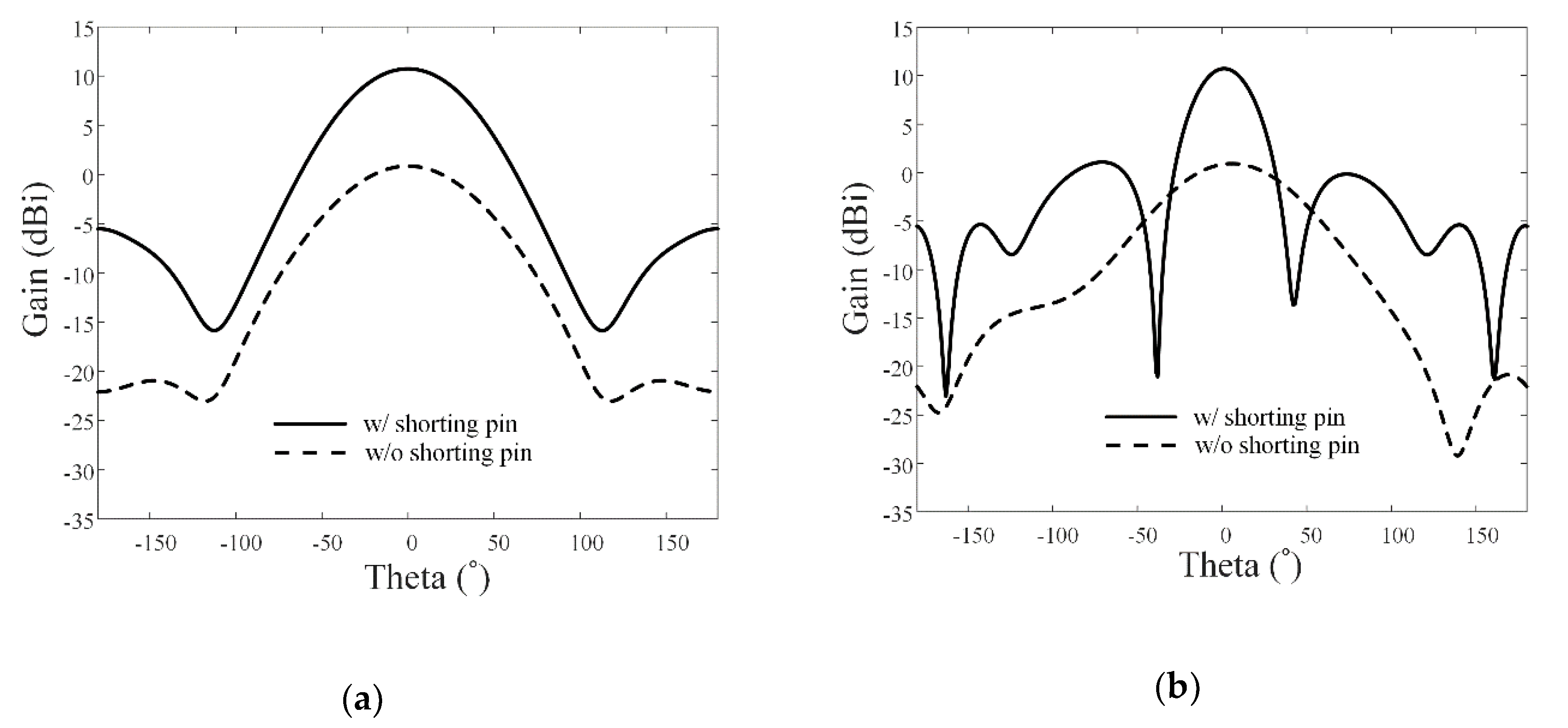
Figure 3 shows the current distributions on the patch antenna surface with and without shorting pins, which is simulated using the FEKO EM simulation software [28]. The patch antenna without shorting pins operates in the TM010 mode, while the patch with shorting pins can change the current distributions to a high-order mode of TM030. Figure 4 shows the 2-D radiation patterns with and without the shorting pins. The simulated bore-sight gains with and without shorting pins are 10.7 dBi and 7.9 dBi, respectively. These results show that the patch antenna with metallic shorting pins can improve bore-sight gain by about 2.8 dB using the high-order mode operation.
Figure 5 illustrates the Fabry–Perot structure consisting of a perfect electric conductor (PEC) surface and a superstrate placed at a height h. The complex reflection coefficients of the PEC surface and the superstrate are ejφ1 and pejφ2, where p is the amplitude, and φ1, φ2 are the reflection phases. The superstrate is a partially reflective surface, and we assume there is no transmission loss. The excited electromagnetic waves by a source are partially reflected by the superstrate and partially transmitted through the superstrate. The electric field intensities outside the Fabry–Perot structure are then obtained by the vector sum of multiple rays, as expressed in Equation (1) [29,30]
The phase angle θn is calculated by the phase variation from the PEC surface to the superstrate, and also by the path differences of the multiple reflections, as shown in Equation (2),
where λ is the wavelength of the target frequency. The power pattern S can be defined as follows:
where f(α) is the function of the antenna pattern in the direction α. Therefore, h can be written as
and we found that h is 23 mm in our geometry at 5.8 GHz.
Figure 6 shows the 2-D radiation patterns with and without the superstrate. The simulated bore-sight gain with the superstrate is 13.8 dBi, whereas it is 10.7 dBi without the superstrate. These results show that the superstrate can improve the bore-sight gain by 3.1 dB using Fabry–Perot theory.
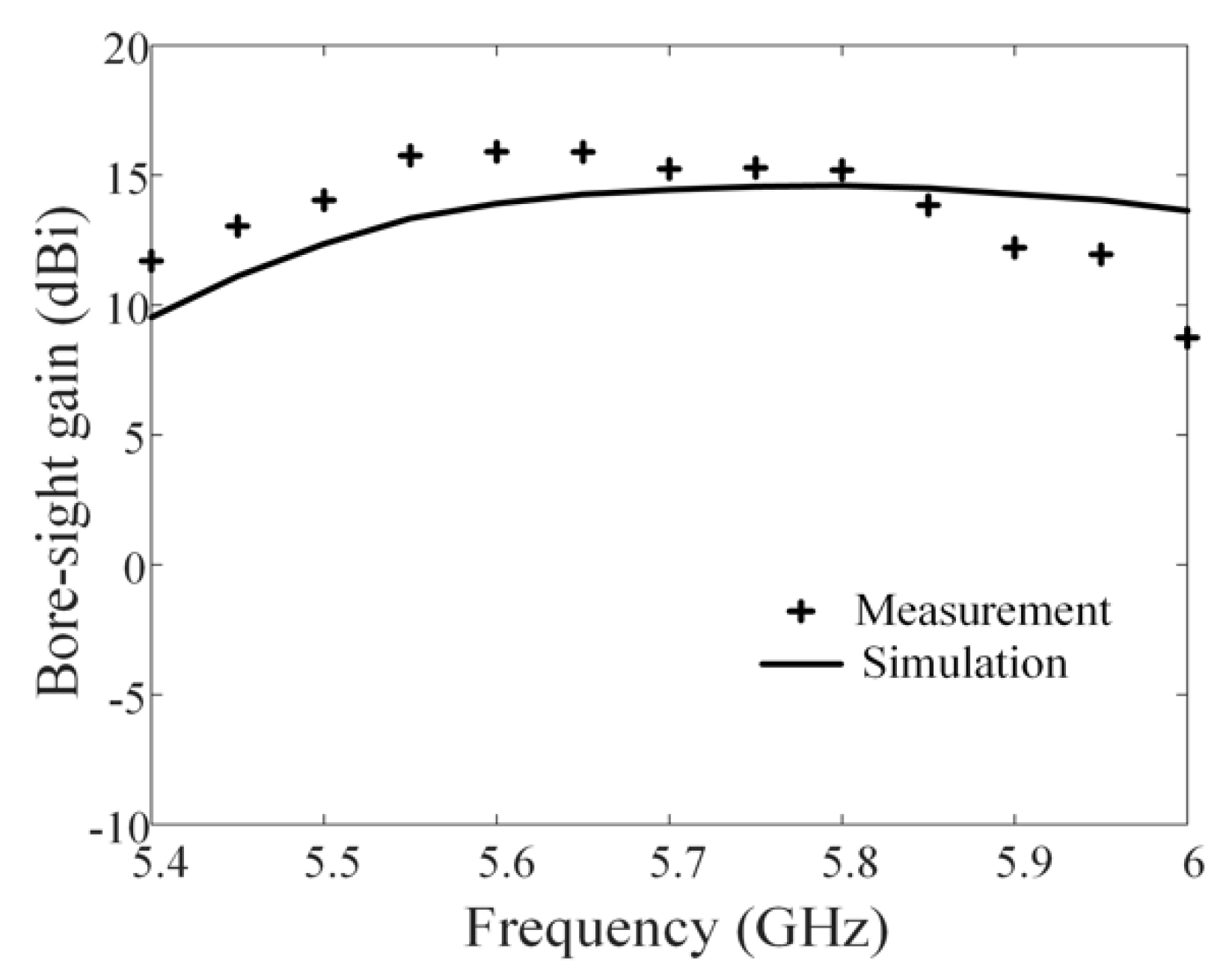
Figure 7 shows the measured and simulated reflection coefficients of the proposed antenna element. The solid line and “+” symbol indicate the simulation and the measurement, respectively. The simulated value of −15.3 dB is in good agreement with the measured value of −23.2 dB at 5.8 GHz. The measured and simulated bore-sight gains are 15.2 dBi and 14.5 dBi at 5.8 GHz, respectively, and they are greater than 8 dBi over the entire range of 5.4–6 GHz, as shown in Figure 8. This result indicates that the gain is improved 6.6 dB over the patch antenna without shorting pins. There is some discrepancy between simulation and measurement, which is due to slight variations in the effective dielectric constant and manufacturing errors of the thick superstrate.
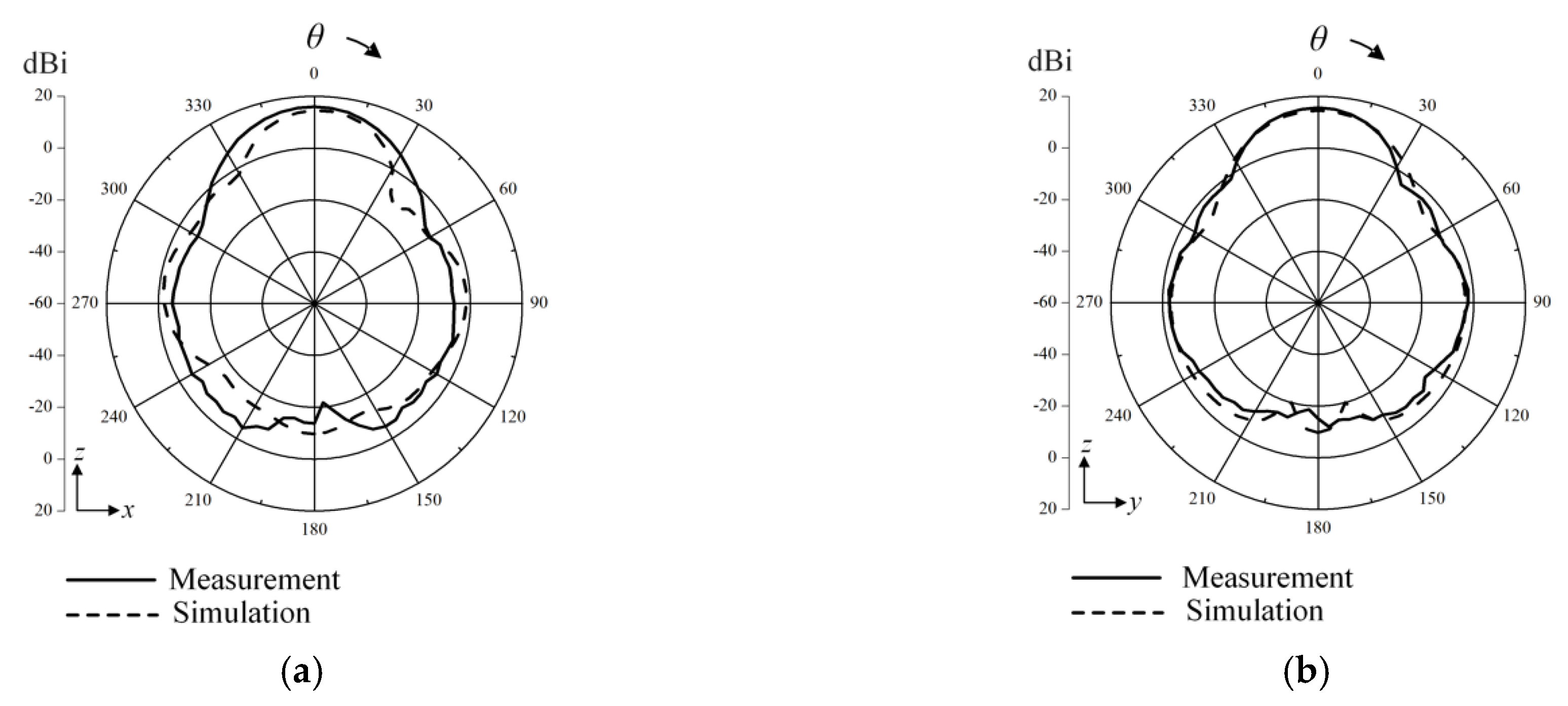
Figure 9 shows the 2-D radiation patterns of the antenna in the zx- and zy-planes. For accurate measurement, the antenna is mounted on a Styrofoam with a 3-axis positioner in a full anechoic chamber. The measured half-power beamwidths at 5.8 GHz are 30° in the zx-plane and 35° in the zy-plane.
3. Array Extension and Performance Analysis
3.1. 2 × 2 Array Extension
The proposed antenna is then extended to a 2 × 2 array, as shown in Figure 10a. We used the 4-way power dividers as the feeding network, as shown in Figure 10b. These dividers were used for the feeding network of the 2 × 2 array as well as the 4 × 4 array. To maximize the performance of the array for wireless power transmission applications, an optimal design of the array is carried out to maximize the array aperture efficiency. The aperture efficiency η of the array can be written as
where Aem is the effective maximum area of the array, and Aphysical is the physical area (A22) of the array aperture. The effective maximum area Aem can be written as
where λ and G represent the wavelength and the antenna gain, respectively.
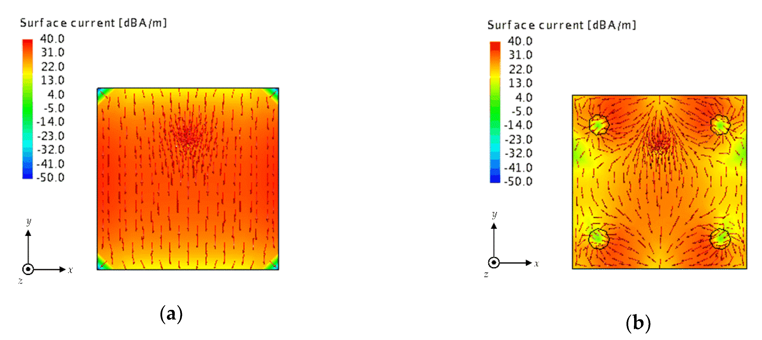
Figure 10c shows the aperture efficiency according to the distance d2 between adjacent elements at 5.8 GHz. The solid line and dashed line indicate the aperture efficiencies with and without the extended cavity structure, respectively. The maximum aperture efficiencies with and without the cavity structure are 74.2% (d2 = 7.5 mm) and 61.2% (d2 = 2.5 mm), respectively. Additionally, the maximum aperture efficiency of the array without shorting pins is 22.05% (d2 = 0 mm). To analyze the effectiveness of the proposed extended cavity structure, we observe the E-field distributions (Ey) on the 2 × 2 array surface (−75 mm ≤ x, y ≤ 75 mm) at z = 57.6 mm with and without the cavity, as shown in Figure 11. The variance value is then calculated from the E-field distributions when an input power of 1 W is used. The variance of the proposed array is 163.6, which is 334.9 lower than the variance of 498.5 without the extended cavity structure. The results demonstrate that the extended cavity structure can lead to more uniform E-field distributions, which can improve aperture efficiency.
Subsequently, we analyze the effect of the extended cavity structure on the beam characteristics of the array. For this purpose, the bore-sight gains of the active element pattern according to d2 are examined, as shown in Figure 12a. The maximum bore-sight gain of 14.1 dBi (d2 = 15 mm) is observed for the proposed antenna with the cavity structure, whereas the maximum bore-sight gain of 12.7 dBi (d2 = 2.5 mm) is observed without the cavity structure. Figure 12b shows the error in the bore-sight beam direction depending on d2, where the ideal beam direction is θ = 0° in the active element pattern. Herein, the proposed antenna has an asymmetric feeding structure, which causes deviations in the bore-sight beam direction. The proposed array antenna has a lower than 1.2° of the average errors when varying d2 from 0 mm to 20 mm, which is much less than the average error of 9.1° without the cavity structure. To further validate the effect of the extended cavity structure, we examine the average mutual couplings (|S21|, |S31|, and |S41|) of the 2 × 2 array according to d2, as shown in Figure 12c. We also measure the coupling using network analyzer (HP3753D). Port 1 of the network analyzer is connected to the upper left antenna in the array, and Port 2 is connected to the other three antennas one at a time. Except for the two measuring antennas, the other antennas are terminated by 50 Ω. The measured average mutual coupling between antennas is −32 dB, and the simulation value is −34 dB when d2 = 7.5 mm. The proposed array antenna with the cavity structure again shows a lower mutual coupling than the array without the cavity structure. These results demonstrate that the extended cavity structure can minimize the mutual coupling strength between adjacent elements, resulting in an increased bore-sight gain with a low error in the bore-sight beam direction.
Figure 13 shows the simulated and measured radiation patterns of the proposed 2 × 2 array, which is fed by a 4-way power divider. The maximum measured gains are 19.9 dBi in the zx-plane and 18.8 dBi in the zy-plane. The simulated maximum gain is 20.0 dBi in both the zx- and zy-planes. The measured and simulated half-power beamwidths are 14.4° and 14.1° in the zx-plane, while 15° and 14.5° in the zy-plane. In the zy-plane, the simulated radiation pattern is not symmetrical with respect to 0°, and this is due to the asymmetric feeding structure of the array antenna.
3.2. 4 × 4 Array Extension
To achieve higher gain characteristics, we extend the proposed antenna to a 4 × 4 array, as shown in Figure 14a. Figure 14b shows the aperture efficiency according to the distance d4, and the maximum aperture efficiency of 80.5% is achieved when d4 is 0 mm. Figure 15a,b show the measured and simulated array patterns of the 4 × 4 array at 5.8 GHz, and Figure 15c presents the fabricated 4 × 4 array. The measurements are conducted in a full-anechoic chamber, and each antenna is fed by the 4-way power dividers, as shown in Figure 15c. The measured and simulated maximum gains are 24.3 dBi and 26.2 dBi in the zx-plane, while 24.5 dBi and 26.2 dBi in the zy-plane, respectively. The measured and simulated half-power beamwidths are 7° and 8° in the zx-plane, while 9° and 8° in the zy-plane, respectively.
To investigate the efficiency of wireless power transfer between antennas in free space, we set up the system consisting of the transmitter (Tx) with the proposed 4 × 4 array and the receiver (Rx) with a single element. Instead of using a probe, we use the identical single element for the Rx. Since the power transmission is for indoor environment, the distance in the transmission efficiency measurement is less than 2 m, that is in the near-radiating zone, as shown in Figure 16a. We calculate the transmission efficiency using formula as written (Equation (7)). The measured and simulated maximum transmission efficiencies are 6% and 7%, respectively, when the distance between Rx to Tx is 0.8 m. We also compare the properties between the proposed antenna and three reference previous research. In this comparison, we examine the operating frequency, aperture size, and the transmission efficiency. The detailed explanations are given in Table 2.
4. Conclusions
An array antenna with a high aperture efficiency was proposed by employing an array element operating in a high-order mode to improve the transmission efficiency for wireless power transmission applications. The proposed array element consisted of a square patch with four metallic shorting pins, an extended cavity, and a high dielectric superstrate. The proposed array element characteristics, such as the reflection coefficient, bore-sight gain, and radiation patterns, of the proposed antenna were measured, and the average reflection coefficient was −15.0 dB with a bandwidth of 400 MHz (5.6 GHz to 6 GHz, |Γ| < −10 dB). The bore-sight gains were 15.2 dBi, and the measured half-power beamwidths were 30° in the zx-plane and 35° in the zy-plane. The proposed antenna element was extended to 2 × 2 and 4 × 4 arrays, resulting in aperture efficiencies of 74.2% and 80.5%, respectively. The maximum measured gains of 19.9 dBi in the zx-plane and 18.8 dBi in the zy-plane for the 2 × 2 array and 24.3 dBi in the zx-plane and 24.5 dBi in the zy-plane for the 4 × 4 array are observed in a full- anechoic chamber. The transmission efficiency of 6% with a distance of 0.8 m between the Rx and the Tx was measured when setting up the wireless power transfer system consisting of the Tx with the proposed 4 × 4 array and the Rx with a single element.
Author Contributions
Conceptualization, E.K., J.H and H.C.; measurements, E.K.; simulation, E.K.; validation, E.K., J.H and H.C.; formal analysis, E.K. and J.H.; investigation, E.K; writing—original draft preparation, E.K. and J.H.; writing—review and editing, J.H., H.L. and H.C.; visualization, E.K.; supervision, H.C.; project administration, C.S.; funding acquisition, C.S. All authors have read and agreed to the published version of the manuscript.
Funding
“This research was funded by the National Research Foundation of Korea (NRF), grant number NRF-2017R1A5A1015596, No.2015R1A6A1A03031833, and NRF-2017R1D1A1B04031890” and “The APC was funded by NRF-2017R1A5A1015596”.
Acknowledgments
This work was supported by the Basic Science Research Program through the National Research Foundation of Korea (NRF) funded by the Ministry of Education (No. NRF-2017R1A5A1015596) and the NRF grant funded by the Korea government (No.2015R1A6A1A03031833; NRF-2017R1D1A1B04031890).
Conflicts of Interest
The authors declare no conflict of interest.
References
- Park, J.; Kim, D.; Hwang, K.; Park, H.H.; Kwak, S., II; Kwon, J.H.; Ahn, S. A Resonant Reactive Shielding for Planar Wireless Power Transfer System in Smartphone Application. IEEE Trans. Electromagn. Compat. 2017, 59, 695–703. [Google Scholar] [CrossRef]
- Li, S.; Mi, C.C. Wireless power transfer for electric vehicle applications. IEEE J. Emerg. Sel. Top. Power Electron. 2015, 3, 4–17. [Google Scholar]
- Liu, X.; Zhang, F.; Hackworth, S.A.; Sclabassi, R.J.; Sun, M. Wireless power transfer system design for implanted and worn devices. In Proceedings of the Bioengineering, Proceedings of the Northeast Conference, Boston, MA, USA, 3–5 April 2009; pp. 1–2. [Google Scholar]
- Ahn, C.-J.; Kamio, T.; Fujisaka, H.; Haeiwa, K. Prototype of 5.8 GHz Wireless Power Transmission System for Electric Vehicle System. In Proceedings of the 2nd International Conference on Environmental Science and Technology, Singapore, 26–28 Feburary 2011; pp. 1–5. [Google Scholar]
- Park, J.; Kim, J.; Shin, Y.; Park, B.; Kim, W.S.; Cheong, S.J.; Ahn, S. Toroidal-shaped coils for a wireless power transfer system for an unmanned aerial vehicle. J. Electromagn. Eng. Sci. 2019, 19, 48–55. [Google Scholar] [CrossRef]
- Kim, Y.; Boo, S.; Kim, G.; Kim, N.; Lee, B. Wireless power transfer efficiency formula applicable in near and far fields. J. Electromagn. Eng. Sci. 2019, 19, 239–244. [Google Scholar] [CrossRef]
- Campi, T.; Cruciani, S.; De Santis, V.; Maradei, F.; Feliziani, M. Near field wireless powering of deep medical implants. Energies 2019, 12, 2720. [Google Scholar] [CrossRef] [Green Version]
- Brown, W.C. The History of Power Transmission by Radio Waves. IEEE Trans. Microw. Theory Tech. 1984, 32, 1230–1242. [Google Scholar] [CrossRef] [Green Version]
- Hansen, R.C. Focal Region Characteristics of Focused Array Antennas. IEEE Trans. Antennas Propag. 1985, 33, 1328–1337. [Google Scholar] [CrossRef]
- Li, P.F.; Qu, S.W.; Yang, S.; Nie, Z.P. Microstrip array antenna with 2-D steerable focus in near-field region. IEEE Trans. Antennas Propag. 2017, 65, 4607–4617. [Google Scholar] [CrossRef]
- Lipworth, G.S.; Hagerty, J.A.; Arnitz, D.; Urzhumov, Y.A.; Nash, D.R.; Hannigan, R.J.; Tegreene, C.T.; Reynolds, M.S. A Large Planar Holographic Refiectarray for Fresnel-Zone Microwave Wireless Power Transfer at 5.8 GHz. In Proceedings of the IEEE MTT-S International Microwave Symposium, Philadelphia, PA, USA, 10–15 June 2018; pp. 1–4. [Google Scholar]
- Yu, S.; Liu, H.; Li, L. Design of near-field focused metasurface for high-efficient wireless power transfer with multifocus characteristics. IEEE Trans. Ind. Electron. 2019, 65, 3993–4002. [Google Scholar] [CrossRef]
- Yang, X.; Geyi, W.; Sun, H. Optimum Design of Wireless Power Transmission System Using Microstrip Patch Antenna Arrays. IEEE Antennas Wirel. Propag. Lett. 2017, 16, 1824–1827. [Google Scholar] [CrossRef]
- Carvalho, A.; Carvalho, N.; Pinho, P.; Georgiadis, A.; Constanzo, A. 5.8 GHz microstrip antennas and array for microwave power transfer. In Proceedings of the 2015 9th European Conference on Antennas and Propagation, Lisbon, Portugal, 13–17 April 2015; pp. 1–5. [Google Scholar]
- Shan, L.; Geyi, W. Optimal design of focused antenna arrays. IEEE Trans. Antennas Propag. 2014, 16, 5565–5571. [Google Scholar] [CrossRef]
- Shinohara, N. Experimental study of large rectenna array for microwave energy transmission. IEEE Trans. Microw. Theory Tech. 1998, 46, 261–268. [Google Scholar] [CrossRef]
- Ren, Y.J.; Chang, K. 5.8-GHz circularly polarized dual-diode rectenna and rectenna array for microwave power transmission. IEEE Trans. Microw. Theory Tech. 2006, 54, 1495–1502. [Google Scholar]
- Ren, Y.J.; Chang, K. New 5.8-GHz circularly polarized retrodirective rectenna arrays for wireless power transmission. IEEE Trans. Microw. Theory Tech. 2006, 54, 2970–2976. [Google Scholar]
- Nishida, K.; Taniguchi, Y.; Kawakami, K.; Homma, Y.; Mizutani, H.; Miyazaki, M.; Ikematsu, H.; Shinohara, N. 5.8 GHz high sensitivity rectenna array. In Proceedings of the 2011 IEEE MTT-S International Microwave Workshop Series on Innovative Wireless Power Transmission: Technologies, Systems, and Applications, Uji, Kyoto, Japan, 12–13 May 2011; pp. 19–22. [Google Scholar]
- Furukawa, M.; Takahashi, Y.; Fujiwara, T.; Mihara, S.; Saito, T.; Kobayashi, Y.; Kawasaki, S.; Shinohara, N.; Fujino, Y.; Tanaka, K.; et al. 5.8-GHz planar hybrid rectenna for wireless powered applications. In Proceedings of the Asia-Pacific Microwave Conference Proceedings, Yokohama, Japan, 12–15 December 2006; pp. 1–4. [Google Scholar]
- Navarro, E.A.; Craddock, I.J.; Paul, D.L. Synthetic dielectrics for planar antenna design. Electron. Lett. 2000, 36, 491–493. [Google Scholar] [CrossRef]
- Navarro, E.A.; Luximon, A.; Craddock, I.J.; Paul, D.L.; Dean, M. Multilayer and conformal antennas using synthetic dielectric substrates. IEEE Trans. Antennas Propag. 2003, 51, 905–908. [Google Scholar] [CrossRef] [Green Version]
- Zhang, X.; Zhu, L. Gain-Enhanced Patch Antennas with Loading of Shorting Pins. IEEE Trans. Antennas Propag. 2016, 64, 3310–3318. [Google Scholar] [CrossRef]
- Liu, N.W.; Zhu, L.; Choi, W.W. A Differential-Fed Microstrip Patch Antenna with Bandwidth Enhancement under Operation of TM10 and TM30 Modes. IEEE Trans. Antennas Propag. 2017, 65, 1607–1614. [Google Scholar] [CrossRef]
- Yang, Z.J.; Zhu, L.; Xiao, S. An implantable wideband circularly polarized microstrip patch antenna via two pairs of degenerate modes. IEEE Access 2019, 7, 4239–4247. [Google Scholar] [CrossRef]
- Anguera, J.; Andújar, A.; Jayasinghe, J.W. High-Directivity Microstrip Patch Antennas Based on TModd-0 Modes. IEEE Antennas Wirel. Propag. Lett. 2020, 19, 39–43. [Google Scholar] [CrossRef]
- Anguera, J.; Montesinos, G.; Puente, C.; Borja, C.; Soler, J. An undersampled high-directivity microstrip patch array with a reduced number of radiating elements inspired on the sierpinski fractal. Microw. Opt. Technol. Lett. 2003, 2, 100–103. [Google Scholar] [CrossRef]
- FEKO EM Simulation Software, Altair Engineering Inc. 2018. Available online: http://www.altair.co.kr (accessed on 30 April 2020).
- Von Trentini, G. Partially Reflecting Sheet Arrays. IRE Trans. Antennas Propag. 1956, 4, 666–671. [Google Scholar] [CrossRef]
- Liu, H.; Lei, S.; Shi, X.; Li, L. Study of antenna superstrates using metamaterials for directivity enhancement based on fabry-perot resonant cavity. Int. J. Antennas Propag. 2013, 2013, 209741. [Google Scholar] [CrossRef]
Figure 1.
Geometry of the proposed antenna: (a) Isometric view, (b) top view, and (c) side view.

Figure 2.
Photographs of the fabricated antenna: (a) Antenna parts, (b) fabrication of the metallic shorting pins, (c) assembly process, and (d) top and bottom views of the fully assembled antenna.
Figure 2.
Photographs of the fabricated antenna: (a) Antenna parts, (b) fabrication of the metallic shorting pins, (c) assembly process, and (d) top and bottom views of the fully assembled antenna.

Figure 3.
Current distributions: (a) Patch antenna without shorting pins and (b) patch antenna with shorting pins.
Figure 3.
Current distributions: (a) Patch antenna without shorting pins and (b) patch antenna with shorting pins.

Figure 4.
Two-dimensional radiation patterns with and without the shorting pins: (a) zx-plane and (b) zy-plane.
Figure 4.
Two-dimensional radiation patterns with and without the shorting pins: (a) zx-plane and (b) zy-plane.

Figure 5.
Fabry–Perot structure with the superstrate and perfect electric conductor (PEC) surface.

Figure 6.
Two-dimensional radiation patterns with and without the superstrate: (a) zx-plane and (b) zy-plane.
Figure 6.
Two-dimensional radiation patterns with and without the superstrate: (a) zx-plane and (b) zy-plane.

Figure 7.
Simulated and measured reflection coefficients of the proposed antenna.

Figure 8.
Simulated and measured bore-sight gains of the proposed antenna.

Figure 9.
Two-dimensional radiation patterns of the proposed antenna at 5.8 GHz: (a) zx-plane, (b) zy-plane, (c) measurement setup in a full-anechoic chamber, and (d) assembled array element.
Figure 9.
Two-dimensional radiation patterns of the proposed antenna at 5.8 GHz: (a) zx-plane, (b) zy-plane, (c) measurement setup in a full-anechoic chamber, and (d) assembled array element.


Figure 10.
2 × 2 array and aperture efficiency: (a) Geometry of the 2 × 2 array, (b) 4-way power divider, and (c) aperture efficiency according to d2.
Figure 10.
2 × 2 array and aperture efficiency: (a) Geometry of the 2 × 2 array, (b) 4-way power divider, and (c) aperture efficiency according to d2.

Figure 11.
Distributions of the average tangential E-field on the surface (z = 57.6 mm).

Figure 12.
Effect of the extended cavity structure: (a) Bore-sight gain according to d2, (b) error in the bore-sight direction depending on d2, and (c) mutual couplings according to d2.
Figure 12.
Effect of the extended cavity structure: (a) Bore-sight gain according to d2, (b) error in the bore-sight direction depending on d2, and (c) mutual couplings according to d2.

Figure 13.
Measured and simulated radiation patterns: (a) zx-plane, (b) zy-plane.

Figure 14.
The 4 × 4 array and aperture efficiency: (a) Geometry of the 4 × 4 array and (b) aperture efficiency according to d4.
Figure 14.
The 4 × 4 array and aperture efficiency: (a) Geometry of the 4 × 4 array and (b) aperture efficiency according to d4.

Figure 15.
Measured and simulated radiation patterns: (a) zx-plane, (b) zy-plane, (c) fabricated array antenna, (d) feeding network, and (e) measurement setup in a full-anechoic chamber.
Figure 15.
Measured and simulated radiation patterns: (a) zx-plane, (b) zy-plane, (c) fabricated array antenna, (d) feeding network, and (e) measurement setup in a full-anechoic chamber.

Figure 16.
Transmission efficiency: (a) Setup using the proposed antennas and (b) comparison of the simulated and measured transmission efficiencies.
Figure 16.
Transmission efficiency: (a) Setup using the proposed antennas and (b) comparison of the simulated and measured transmission efficiencies.


Table 1.
Design parameters of the proposed antenna.
| Parameters | Optimized Values |
|---|---|
| w1 | 33 mm |
| w2 | 82.5 mm |
| h | 23 mm |
| hs | 7 mm |
| ht | 1.6 mm |
| hc | 5 mm |
| fx | 0 mm |
| fy | 7 mm |
| d | 4 mm |
| px1 | −9.5 mm |
| px2 | 9.5 mm |
| px3 | 9.5 mm |
| px4 | −9.5 mm |
| py1 | 8.8 mm |
| py2 | 8.8 mm |
| py3 | −8.8 mm |
| py4 | −8.8 mm |
© 2020 by the authors. Licensee MDPI, Basel, Switzerland. This article is an open access article distributed under the terms and conditions of the Creative Commons Attribution (CC BY) license (http://creativecommons.org/licenses/by/4.0/).
Share and Cite
MDPI and ACS Style
Kang, E.; Hur, J.; Seo, C.; Lee, H.; Choo, H. High Aperture Efficiency Array Antenna for Wireless Power Transfer Applications. Energies 2020, 13, 2241. https://doi.org/10.3390/en13092241
AMA Style
Kang E, Hur J, Seo C, Lee H, Choo H. High Aperture Efficiency Array Antenna for Wireless Power Transfer Applications. Energies. 2020; 13(9):2241. https://doi.org/10.3390/en13092241
Chicago/Turabian StyleKang, Eunjung, Jun Hur, Chulhun Seo, Hojin Lee, and Hosung Choo. 2020. "High Aperture Efficiency Array Antenna for Wireless Power Transfer Applications" Energies 13, no. 9: 2241. https://doi.org/10.3390/en13092241
Note that from the first issue of 2016, this journal uses article numbers instead of page numbers. See further details here.