
Real-Time Data Acquisition and Processing System for MHz Repetition Rate Image Sensors
by
 , , , , and
Aleksander Mielczarek
1,* ,
,
Dariusz Radosław Makowski
1,
Christopher Gerth
2,
Bernd Steffen
2,
Michele Caselle
3 and
Lorenzo Rota
3,4 1
Department of Microelectronics and Computer Science (DMCS), Łódź University of Technology (TUL), 93-005 Łódź, Poland
2
Deutsches Elektronen-Synchrotron (DESY), 90-924 Hamburg, Germany
3
Karlsruher Institut für Technologie (KIT), 76-131 Karlsruhe, Germany
4
SLAC National Accelerator Laboratory, Menlo Park, CA 94025, USA
*
Author to whom correspondence should be addressed.
Energies 2021, 14(21), 7403; https://doi.org/10.3390/en14217403
Submission received: 30 September 2021
/
Revised: 28 October 2021
/
Accepted: 1 November 2021
/
Published: 6 November 2021
(This article belongs to the Special Issue Selected Papers from 28th International Conference on Mixed Design of Integrated Circuits and Systems—MIXDES 2021)
Abstract
:An electro-optic detector is one of the diagnostic setups used in particle accelerators. It employs an electro-optic crystal to encode the longitudinal beam charge profile in the spectrum of a light pulse. The charge distribution is then reconstructed using data captured by a fast spectrometer. The measurement repetition rate should match or exceed the machine bunching frequency, which is often in the range of several MHz. A high-speed optical line detector (HOLD) is a linear camera designed for easy integration with scientific experiments. The use of modern FPGA circuits helps in the efficient collection and processing of data. The solution is based on Xilinx 7-Series FPGA circuits and implements a custom latency-optimized architecture utilizing the AXI4 family of interfaces. HOLD is one of the fastest line cameras in the world. Thanks to its hardware architecture and a powerful KALYPSO sensor from KIT, it outperforms the fastest comparable commercial devices.
1. Introduction
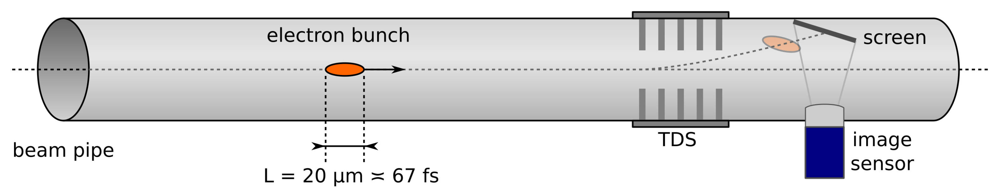
One of the indicators of an accelerator’s performance is its beam current. To maximize this figure, the electron bunches traveling along the accelerator beam pipe must be kept as short as possible. In the case of the European X-ray Free-Electron Laser (EuXFEL) [1] operated by Deutsches Elektronen-Synchrotron (DESY), the lateral length of a bunch is around 20 µm. The bunch leaves the accelerator with a nominal energy of 17.5 GeV, which means that electrons travel at the speed of 0.9999999996 c (every single electron has kinetic energy comparable to a falling snowflake).
To obtain an overview of a beam composition, it is essential to evaluate the longitudinal electric charge distribution in these packets of 20 µm length. Several methods of measuring the bunch longitudinal charge profile have been developed, such as with the use of transverse deflecting structures (TDS) [2]. The idea behind them is briefly illustrated in Figure 1. A TDS can kick a single bunch out of the bunch train, directing it to an off-axis screen while, at the same time, applying yaw to it. The charge is deposited along the screen, which is in turn observed by an image sensor.
Although diagnostics based on TDS is a powerful tool, it is also a destructive one. It is not possible to measure a particular bunch and then use it in an experiment. This problem is solved by the use of electro-optic detectors (EODs), which allow the performance of a nondestructive real-time evaluation [3]. The EOD installed at EuXFEL employs such a method. It uses an electro-optic crystal, located around 6 mm from the beam path, to encode the beam charge density profile on the spectrum of an IR laser pulse (1050 µm). The longitudinal charge distribution is then reconstructed using data from a fast spectrometer [4].
2. Acquisition System Requirements
The EOD spectrometer should ideally operate with a repetition rate equal to the machine bunching frequency. In the case of the EuXFEL accelerator, this would mean reaching a frame rate of 4,500,000 frames per second (FPS). The EOD optical setup was earlier read by the Integrated Radiation Spectrometer [5,6], which was only capable of capturing around 1,000,000 FPS. The aim of the new detector is to maintain the spatial resolution and analog precision of the predecessor while pushing the frame rate limit at least to half of the EuXFEL bunching frequency (~2.25 MHz). The detector has to provide 256 readout channels, with 50 µm pitch and 14-bit ADC resolution.
For the off-line tuning and performance analysis of the EuXFEL accelerator, the device has to be able to acquire up to 2700 consecutive readouts and provide raw data to the host CPU within 100 ms, before the arrival of the next bunch train [1]. The samples are stored in a buffer with 16-bit alignment. Therefore, the representation of a single bunch train consumes around 1.4 MB of memory.
However, data from the EOD can be used for more than just an off-line evaluation. The samples will be captured fast enough, so that the calculated bunch parameters can be applied for the real-time correction and optimization of the accelerator operation—within the scope of beam-based feedback (BBF). It is desirable to keep the latency between the probing laser pulse and delivery of the processed parameters under 1 µs in order to close an inner low-level radio frequency (LLRF) feedback loop within 2 µs [7].
Since a fast 1D camera can have many other applications in physics experiments, it should be designed in a way that maximizes the chances of reuse. It should support several sensor materials to enable operation in different wavelength regimes. For DESY purposes, the device has to support at least Si (visible light) and InGaAs (infra-red) photodiode arrays. In order to maintain high noise immunity and reduce the number of necessary external components, the sensor bias voltage must be generated locally. Due to the large difference in required polarization voltages for the considered sensor materials, the spectrometer should be equipped with two separate remote-controlled, adjustable, low-noise power supplies—one with an output range of 0–100 V for the silicon sensor and another providing 0–10 V for the InGaAs strip.
Most of the control and diagnostic systems of EuXFEL are realized in the MicroTCA.4 architecture [8]. This is a platform that supports high reliability, availability, maintainability, and inspectability (RAMI). Its specification defines the electrical, thermal, and mechanical requirements for the boards and crates that host them [9]. Compliance with the standard is vital for ensuring seamless integration with the other systems of the accelerator. In the case of an upgrade or some failure, MicroTCA.4-compliant modules can be easily replaced without disturbing other systems operating in the same crate.
3. Hardware Design
3.1. Overview
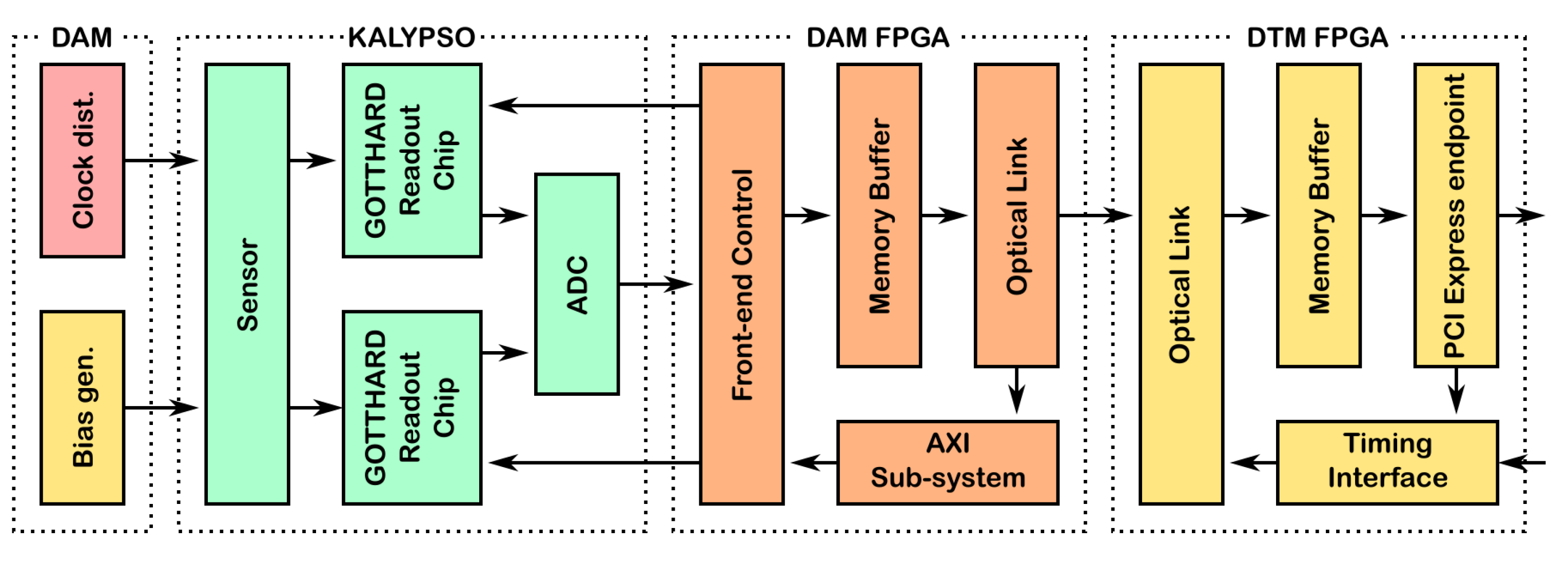
HOLD stands for high-speed optical line detector. It is an ultra-fast linear camera designed for easy integration with scientific experiments. The use of modern FPGA circuits helps in the efficient collection and processing of data. Adoption of an Advanced eXtensible Interface (AXI) architecture enables the use of many stock IP cores and promotes design reuse [10]. The general structure of the solution is depicted in Figure 2. It is composed of the following hardware components:
- Data Acquisition Module (DAM)—an FPGA-based device collecting data, performing computations, and transmitting results over optical fibers;
- Data Transmission Module (DTM)—an MTCA.4 module responsible for capturing the collected data stream and providing it to a host computer.
The architecture with two separate FPGA devices communicating over an optical link (operating at 3.125 Gb/s) is a compromise between having a compact and integrated detector and the requirement to maintain compliance with the MicroTCA.4 standard [13,14].
The DAM provides the sensor module with bias voltages and clock signals. The 256 sensing elements are sampled by two GOTTHARD ASICs [15]. Each ASIC is equipped with 128 charge-sensitive amplifiers, sample-and-hold circuits, and an 8-channel multiplexer. From there, the acquired samples are shifted to an external ADC, digitized, and provided to the DAM FPGA. The DAM FPGA is responsible for controlling the acquisition process and storing the captured samples in the memory. Then, the data are transmitted over an optical link to the DTM FPGA. This second FPGA is responsible for capturing the stream and providing it to the host CPU over the PCIe interface. The optical link also provides a bidirectional memory-mapped control channel.
For the detector to operate synchronously with the machine, it has to be provided with a reference clock and trigger signals. These are supplied from the X2 Timer module through an unshielded twisted-pair (UTP) cable. All boards installed in the crate communicate with the CPU module using a PCIe interface. This is the main interface for both control and data transmissions. The crate also contains a power supply unit (PSU) and a MicroTCA Carrier Hub (MCH)—responsible for power and thermal management of modules as well as for the provision of PCIe and Ethernet switches. The HOLD system installed in a crate is presented in Figure 3.
3.2. Data Acquisition Module
The DAM is an FPGA Mezzanine Card (FMC) carrier with a single high-pin-count connector, dedicated to supporting the KALYPSO detector. The KALYPSO board integrates a photodiode array, two GOTTHARD readout chips, a jitter attenuating PLL, and an ADC circuit. GOTTHARD is a bare die readout circuit for photo-detectors. It contains 128 charge-sensitive input channels multiplexed to 8 analog differential outputs. Two such integrated circuits are used to read the whole line of 256 pixels. The GOTTHARD chips are still actively being developed and the KALYPSO module is expected to evolve with them.
The 16-channel 14-bit ADC captures data from both front-end chips simultaneously. Each converter channel is connected to the FPGA using only a single digital differential pair. The data are serialized at a ratio of 14:1, generating a stream of around 756 Mb/s per lane (sampling clock of 54 MHz, approximately 12 Gb/s of total throughput). The ADC also returns a delayed version of the reference clock, as well as a 7-times faster clock, to be used during the deserialization process. The DAM fitted with the KALYPSO detector is shown in Figure 4.
The DAM structure is presented in Figure 5. It is based on a Xilinx 7-Series FPGA device, which provides the processing power and a number of high-performance interfaces. The FPGA is equipped with a quad multi-gigabit optical link implemented with the use of small form-factor pluggable (SFP) transceivers. This interface is used for control, for raw data streaming, as well as for a low-latency communication channel to the LLRF system. The whole link is capable of providing throughput of up to 26 Gbps (four channels of up to 6.5 Gb/s).
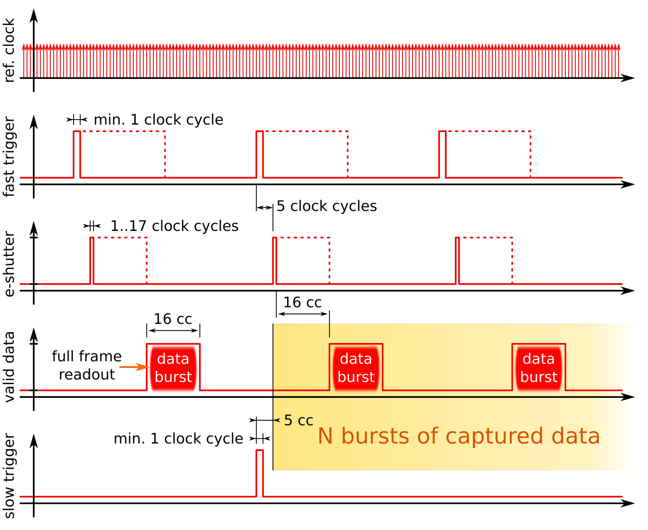
Timing signals are provided to the HOLD by a dedicated timer module (DESY X2 Timer). These include a reference clock and two triggers. The signals are carried by a twisted-pair cable, with the use of LVDS signaling. First, the jitter in the clock signal is attenuated by a phase-locked loop (PLL). The resulting clean clock is provided to the FPGA and to the KALYPSO mezzanine. The “fast” trigger enables the charge collection process and therefore effectively starts the acquisition of a single image frame. It is expected to arrive synchronously with the light pulse on the sensor. Introducing additional “fast” trigger pulses enables the capture of dark frames and tracking of the detector baseline. The “slow” 10 Hz trigger is used to mark the start of the next macro-pulse of the accelerator. It enables the acquisition of a block of a configurable number of frames. The DAM is equipped with a 64-bit DDR3 memory bank of 2 GB. However, only a small fraction of this storage is ever used, because the data are immediately streamed to the DTM. The time relationship between the trigger and the front-end operation is shown in Figure 6. For development purposes, both the triggers and clock can be also generated internally.
The photodetector sensitivity strongly depends on its bias voltage. Therefore, this parameter has to be controllable remotely. This feature is implemented through two linear adjustable power supplies based on high-output current operational amplifiers. One is dedicated to the InGaAs detector and provides voltage in the range of 0–10 V. The other one is used with Si photodiodes and can provide up to 120 V. In order to keep power losses relatively low, it is powered by an adjustable DC/DC boost converter, which can generate voltages of up to 140 V. The power supply functionality is controlled by a dedicated micro-controller, which communicates with the FPGA over UART.
3.3. Data Transmission Module
The DTM is based on the MFMC module—a carrier board with two FMC slots and a recent 7-Series Xilinx Artix FPGA. The MFMC board contains a DDR3 SDRAM bank of 2 GB composed of four 16-bit chips. The 64-bit DDR bus can be operated at up to 533 MHz, providing a throughput of around 68 Gb/s. The board interfaces the shelf with PCIe x4 gen. 2 and an M-LVDS bus. The optical link to the DAM is implemented with the use of a dedicated FMC daughter board.
4. HOLD Firmware
4.1. Data Acquisition Module
The data path of DAM firmware starts with a block capturing the data stream from an ADC circuit. Part of the firmware responsible for this process is presented in Figure 7.
In order for the ADC to provide valid signal samples, it has to be first configured through an SPI bus. A finite state machine sending a series of hard-coded words is used to select the desired operation mode and optionally activate one of the available link test patterns. The ADC transmits data to the FPGA in the double data rate (DDR) mode. To ensure a correct sampling point, data received by the FPGA are routed through the IDELAY stages. These introduce small adjustable delays in the data path. The optimal setting for these components was found using several link training patterns provided by the ADC. After deserialization, the data are stored in a shallow FIFO, which is used to reliably transfer the samples to the main clock domain.
Setting an optimal sampling point for signals from the GOTTHARD chips requires the ADC clock phase to be adjustable in relation to the front-end clock. This is fulfilled by the provision of a phase shifter based on a Mixed-Mode Clock Manager (MMCM) primitive. This component is capable of performing a variable phase shift with a resolution of around 0.3° and covering the full 360° range.
The ADC captures a new set of samples in every clock cycle, regardless of the GOTTHARD chip state. To determine which samples carry meaningful data, the reader module utilizes a dedicated signal from the GOTTHARD chip control logic. The signal indicates that the chip is actively driving its outputs. This signal is then delayed by the same number of cycles as is needed by the ADC to perform the conversion and by the FPGA to latch its results (~15 cycles). Afterwards, it is used to generate the AXI Stream flags (TVALID and TLAST) that accompany the received data. The resulting bursts of valid data words are marked with red bubbles in Figure 6.
The GOTTHARD readout chip has no master clock. The control signals are processed immediately. In order to synchronize the chip with the accelerator timing, it is driven by a state machine implemented in the FPGA. The state machine is responsible for controlling the integrator, the sample-and-hold circuit, and the readout multiplexer. The readout sequence is triggered by the external “fast” trigger, synchronous to the machine bunching frequency. It is used to synchronize the acquisition process with the arrival of light pulses from the measurement setup.
Samples from the analog front-end are captured continuously. However, these are only marked as valid and stored in the memory after the occurrence of a second trigger from the timing module. This “slow” trigger arrives before each macro-pulse of the machine. From its active edge, a predefined number of full sensor readouts is passed to the HOLD data pipeline (highlighted with an orange background in Figure 6). EuXFEL is expected to operate with up to 2700 bunches per macro-pulse. In order to provide a considerable margin for the forthcoming machine upgrades, the HOLD firmware was designed to be capable of capturing up to 10,000 lines per shot.
The data acquisition module firmware structure is presented in Figure 8. The design is composed of a number of reusable blocks interfacing with AXI buses.
Data from the ADC are provided with a header disclosing the number of acquired samples and the sequential number of the current machine pulse. Next, the captured frame is transferred to a buffer implemented in DDR3 memory. If the buffer is currently full, a complete frame is discarded.
Simultaneously, captured data can be also transferred to the other path, highlighted with a green background. This path is focused on providing data for the BBF system. This part of the design is still under development. Its purpose is to compute a number of parameters characterizing the bunch charge distribution—in particular, the position of the center-of-mass, the lateral spread of the pulse, and the mean pixel readout. The calculated values will be delivered to the LLRF system over a dedicated optical fiber.
Data from the memory buffer are divided into packets of 32 bytes and sent over an optical link. The link utilizes a DESY proprietary low latency link (LLL) protocol. The LLL frames are composed of a simple header, payload data, and a checksum. As the name implies, the protocol is focused on minimizing the transfer latency. This optimization comes at the cost of a fixed (compile-time selected) frame length and lack of support for the repetition of corrupted frames. The DESY FPGA firmware framework provides convenient means for multiplexing several data streams over one link. It is also possible to tunnel a memory-mapped bus through an LLL link. This feature is used to expose the DAM registers in the DTM address space. These registers offer control over the acquisition block, ADC, GOTTHARD chips, and the bias voltage generator.
4.2. Data Transmission Module
The DTM firmware structure is depicted in Figure 9. Data arrive at the DTM through the optical link, from where they are provided to the DAQ block. This module is responsible for converting a stream of data to a series of bursts on a memory-mapped interface. It is used to implement a circular buffer in the DDR3 memory. The readouts stored in the memory are then read by the DMA engine, tightly coupled with the PCIe endpoint block. The PCIe interface is also used for the control of both the DTM and DAM.
The optical link is also used for sending the current machine pulse number to the DAM. This information is received over the MicroTCA.4 backplane via an M-LVDS bus from the X2 Timer module.
The DTM firmware is based on the DESY FPGA framework. However, some of its core components could not be directly used as the framework did not support the Artix-7 family of Xilinx FPGA circuits. Therefore, the LLL interface block, the memory controller, and the PCIe endpoint had to be adapted.
5. HOLD Software
The HOLD software stack is composed of the following components:
- Pcieuni driver—a generic Linux PCIe device driver developed at DESY;
- ChimeraTK—a library for the pcieuni driver, providing device read/write functionality;
- Python class—for debugging and low-level device access;
- C++ class—for integration with the control system;
- GoLive—an on-line control and monitoring application;
- GoView—an off-line data viewer for the collected data;
- GoUp—a firmware upgrade application.
The HOLD DTM firmware was prepared within the DESY FPGA firmware framework and includes the DESY proprietary DMA engine. It co-operates with the DESY standard pcieuni driver and the ChimeraTK access library. A Python class allows register-level access and was mainly used during the development process. However, it can be also considered an interface for accessing the HOLD data and settings from other scripts or simple applications.
Complete functionality of the HOLD solution is exposed by a C++ class. It provides a device-level API and high-level access to I2C, SPI, and UART interfaces. It is a base for demonstration applications as well as the data source for the DOOCS [16] control server developed by DESY. It is accompanied by a set of auxiliary classes encapsulating communication with the PLL circuits on the DAM, bias DACs on the KALYPSO module, and the SPI flash memory.
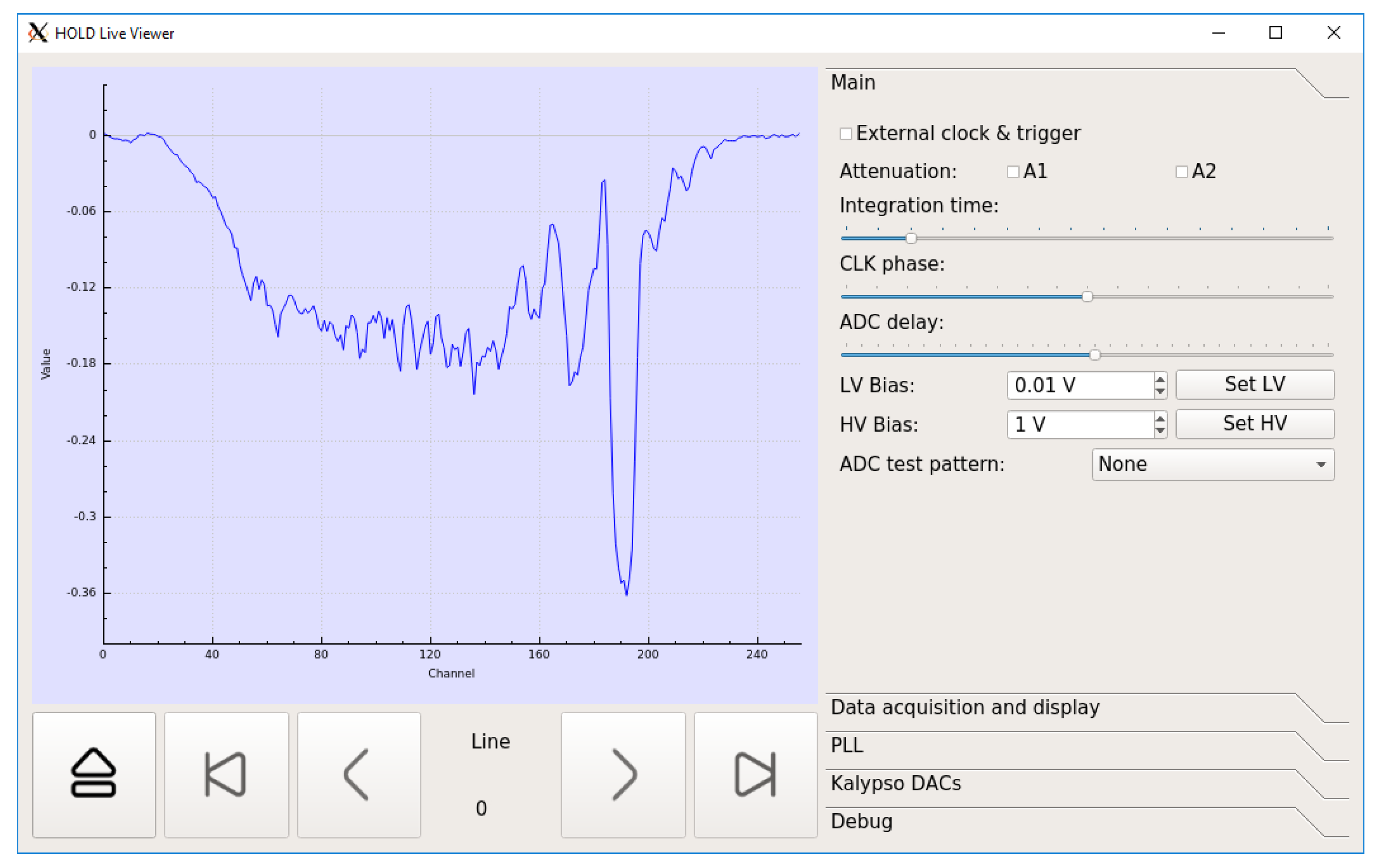
Two GUI applications are provided for convenient verification of the system’s operation and performance. The GoLive utility offers control over the acquisition process, presents readouts in real time, and offers the option of saving to a file a configurable number of device frames. A view of the application window is shown in Figure 10.
The second application, GoView, enables the exploration of the recorded data. It offers a simple interface for navigating through captured lines and frames. It also provides a set of cursors for manual measurements.
Another GUI application is used for convenient programming and verification of the SPI flash memory. This memory holds the FPGA firmware bit file. Its contents may be replaced during the detector operation, without the use of an external programmer. The application is capable of reading the bit file headers, in order to provide some details (e.g., synthesis date) on the bitstream loaded in the memory or stored on a disk.
6. Evaluation of HOLD
Verification of the high-speed optical line detector was divided into three stages:
- Tests and performance evaluation of the data acquisition system using a dummy data generator;
- Operation in the spectrometer configuration with light provided by an LED;
- Verification of operation in the EuXFEL machine.
Analysis of data captured in the EuXFEL is provided in a separate publication [4]. Evaluation of the KALYPSO detector is provided in the papers [11,17].
6.1. Methods of Evaluation
The aim of the first test was to demonstrate the capability of capturing data and transferring them to a host machine over an optical link. During an 8 h test, a simple pattern generator was used to provide bursts of data corresponding to ADC sampling 256 channels with 16-bit resolution at 4.5 million frames per second. The generator served bursts of up to 10,000 frames at 18.4 Gb/s with a 10 Hz repetition rate. The data were buffered in the DDR memory and transferred over an optical link to the DTM, from where they were provided to the CPU. The integrity of the received stream was verified by comparing the frame contents with a known pattern of the dummy data generator. Additionally, the sequence number of each frame was also checked.
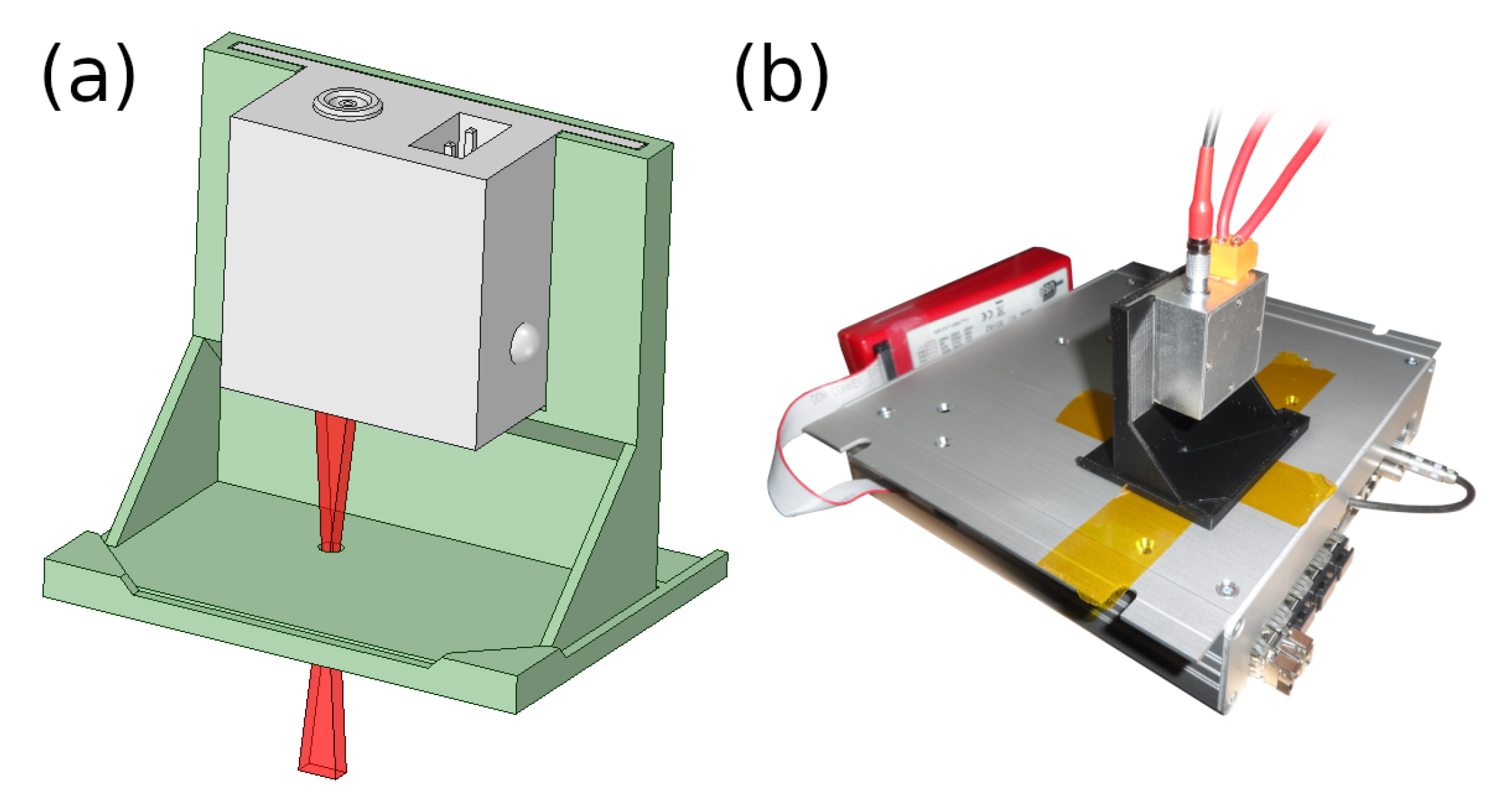
The second test was focused on the general detector operation. Its goal was to demonstrate the capability of performing the acquisition of 1D images. For the test, the front-end was supplied with a 54 MHz clock and configured for capturing frames with a 1 MHz repetition rate. The timing signals were provided by an external FPGA board (a re-purposed DRTM-VM2 module from DESY [18]). Special firmware was developed for it to emulate an X2 Timer module, which is usually used at DESY to provide timing signals to MicroTCA.4 systems. The improvised timing generator also provided a 10 Hz signal to a near-IR (~900 nm) LED light source. The LED was mounted in a 3D-printed fixture, shown in part (a) of Figure 11; this allowed the illumination of only a part of the sensor (around 10 or 60 pixels, depending on the selected slit plate).
The test setup with the detector and a light source is presented in part (b) of the aforementioned figure. Orange strips, visible in the photograph, are pieces of Kapton tape, providing mechanical protection of the detector opening. Just before the LED is turned on, the detector is triggered to take a number of samples (e.g., 20) at 1 µs intervals. Each time, the signal from the sensor is integrated during a time span of a few 54 MHz clock cycles. Further tests of the HOLD were performed in the final spectrometer configuration, which is illustrated in Figure 12.
For this purpose, the spectrometer box was set up at DESY. The HOLD front-end was configured to capture 1 million frames per second. Light pulses were provided by a small table-top laser (CLD101x) through a polarization-maintaining optical cable, visible in the upper right corner of Figure 12. The collimator forms a parallel beam, which is then sent to a diffraction grating, visible in the center of the image. Next, the beam travels through a set of two cylindrical lenses. Finally, it is reflected by a mirror and directed to the DAM, which is mounted in its housing below the baseboard.
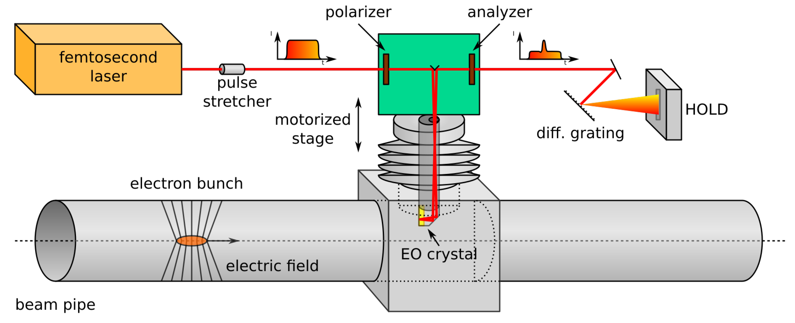
In 2019, the detector was also evaluated at EuXFEL as a part of the spectrally resolved EOD setup, illustrated in Figure 13. It contains a laser generating femtosecond pulses of infrared light (1050 µm), synchronized with the accelerator. These are passed through an optical stretcher, which causes the pulse to last longer and introduces a slight frequency variation over time, known as a “chirp”. The pulse is then polarized and fed through an electro-optic crystal. When the light passes through the crystal, its polarization is rotated as a function of the intensity of the electric field. Afterwards, returning light is analyzed by a second polarizer and directed to a diffraction grating. Finally, the resulting spectrum is directed to the InGaAs photodiode array for readout. As the light frequency changes during the pulse, each wavelength conveys information on an electric field crossing the crystal at a different moment in time. This, knowing the bunch speed, enables the reconstruction of the longitudinal charge profile.
6.2. Results
No integrity problems were observed during the tests. Data were successfully generated, transferred, and verified. However, the tests were concluded with one unforeseen result. The optical link operating at a line rate of only 3.125 Gb/s was expected to constitute the main bottleneck of the design. It utilizes the 8b/10b encoding; hence, its maximum data rate is limited to 2.5 Gb/s. Including the protocol overhead for relatively short packets of 32 data bytes, the link allowed for a payload data transfer rate of around 2.0 Gb/s. The 10,000 line packet was therefore transferred through an optical link in around 20 ms (of 100 ms between consecutive data bursts). Surprisingly, the actual performance limit was superimposed by the card-to-host DMA engine, requiring around 29 ms to complete the transfer (5.12 MB ÷ 29 ms = 176.6 MB/s). The low DMA throughput was caused by the lack of circular buffer support in ChimeraTK. Reading such a structure with ChimeraTk requires the allocation of a dynamically allocated accessor object for each transfer, which takes up to several milliseconds. The tests with the actual detector were initially performed with an InGaAs sensor and a light source providing near-IR light (~1050 nm). An exemplary result from a test with the LED and slit plate is illustrated in Figure 14.
In contrast, the KALYPSO modules equipped with silicon sensors showed unusually large differences between consecutive samples, especially those located at the slopes of the slit-induced Gaussian shape. It was later found that this behavior was caused by a bonding issue, resulting in a swap between odd and even pixels. The adequate correction was eventually implemented in the software.
After the laboratory verification of the complete spectrometer, two HOLD systems were mounted in the EuXFEL accelerator. These now serve as readout devices for EOD setups, evaluating the longitudinal bunch charge profile. These operate with 1.13 MHz and 2.26 MHz measurement repetition rates. The first results from EuXFEL [19] are shown in Figure 15.
The image presents data captured for a single machine pulse composed of 1500 bunches. Each horizontal line represents a charge distribution along a single bunch. The vertical axis corresponds to the line number in a pulse. These lines were captured with 1 µs intervals. The horizontal axis has several interpretations: it corresponds to the light position on the detector, which maps to the wavelength and to the time delay from the laser pulse. More detailed verification of the EOD operation is presented in a separate paper [4].
7. Conclusions and Future Plans
HOLD is one of the fastest line cameras in the world. It is capable of capturing a few million frames per second and hence outperforms the fastest comparable commercial devices. HOLD can be used in place of the legacy GOTTHARD modules developed by Paul Scherrer Institut [15]. In contrast to its predecessor, it offers precise synchronization with the machine timing, lower latency of the main data link (due to no dependency on the IP stack), and the possibility to provide information on the beam directly to the LLRF system.
HOLD firmware was developed in the Xilinx Vivado software suite according to the recent development guidelines. The top-level structure was designed in the form of a block diagram drawn in the IP Integrator. To avoid duplication of effort, well-tested Xilinx IP cores were used whenever possible. This enabled rapid and effective development [20]. The firmware of the data transmission module was prepared using the DESY FPGA firmware framework [21] in accordance with DESY firmware guidelines. The module operates with the driver and the ChimeraTK library, which are already used at DESY.
The current generation of the KALYPSO sensor enables the acquisition of data with a speed of 2.7 million frames per second [11]. The HOLD firmware is currently being adapted for the new KALYPSO module that supports photodiode arrays with up to 1024 photosensitive elements, and it offers improved readout circuits and more powerful ADCs with a JESD204B interface [22].
Author Contributions
Conceptualization, B.S., C.G. and M.C.; Funding acquisition, C.G. and D.R.M.; Investigation, A.M. and L.R.; Methodology, D.R.M.; Resources, M.C.; Software, A.M., D.R.M.; Hardware, A.M., D.R.M. and B.S.; Supervision, D.R.M. and C.G.; Validation, L.R.; Visualization, B.S.; Writing—original draft, A.M.; Writing—review and editing, D.R.M. All authors have read and agreed to the published version of the manuscript.
Funding
This research received no external funding.
Institutional Review Board Statement
Not applicable.
Informed Consent Statement
Not applicable.
Data Availability Statement
Not applicable.
Conflicts of Interest
The authors declare no conflict of interest.
Abbreviations
The following abbreviations are used in this manuscript:
| ADC | Analog-to-Digital Converter |
| ASIC | Application-Specific Integrated Circuit |
| AXI | Advanced eXtensible Interface |
| BBF | Beam-Based Feedback |
| CPU | Central Processing Unit |
| DAM | Data Acquisition Module |
| DDR | Double Data Rate |
| DESY | Deutsches Elektronen-Synchrotron |
| DOOCS | Distributed Object-Oriented Control System |
| DTM | Data Transmission Module |
| EOD | Electro-Optical Detector |
| EuXFEL | European X-ray Free-Electron Laser |
| FCO | Frame Clock Output |
| FIFO | First-In First-Out |
| FMC | FPGA Mezzanine Card |
| FPGA | Field Programmable Gate Array |
| FPS | Frames Per Second |
| HOLD | High-Speed Optical Line Detector |
| IR | Infrared |
| KALYPSO | KArlsruhe Linear arraY detector for MHz rePetition-rate SpectrOscopy |
| KIT | Karlsruher Institut für Technologie |
| LED | Light-Emitting Diode |
| LLL | Low-Latency Link |
| LLRF | Low-Level Radio Frequency |
| MCH | MicroTCA Carrier Hub |
| MM | Memory Mapped |
| MMCM | Mixed-Mode Clock Manager |
| PCIe | Peripheral Component Interconnect Express |
| PLL | Phase-Locked Loop |
| PM | Polarization-Maintaining |
| PSU | Power Supply Unit |
| RAMI | Reliability, Availability, Maintainability, and Inspectability |
| SFP | Small Form-Factor Pluggable |
| SPI | Serial Peripheral Interface |
| TDS | Transverse Deflecting Structure |
| UTP | Unshielded Twisted Pair |
References
- Decking, W.; Abeghyan, S.; Abramian, P.; Abramsky, A.; Aguirre, A.; Albrecht, C.; Alou, P.; Altarelli, M.; Altmann, P.; Amyan, K.; et al. A MHz-repetition-rate hard X-ray free-electron laser driven by a superconducting linear accelerator. Nat. Photonics 2020, 14, 391–397. [Google Scholar] [CrossRef]
- Behrens, C.; Gerasimova, N.; Gerth, C.; Schmidt, B.; Schneidmiller, E.A.; Serkez, S.; Wesch, S.; Yurkov, M.V. Constraints on photon pulse duration from longitudinal electron beam diagnostics at a soft X-ray free-electron laser. Phys. Rev. Special Top. Accel. Beams. 2012, 15, 030707. [Google Scholar] [CrossRef]
- Steffen, B.R. Electro-Optic Methods for Longitudinal Bunch Diagnostics at FLASH. Ph.D. Thesis, Universität Hamburg, Hamburg, Germany, 2007. [Google Scholar]
- Steffen, B.; Gerth, C.; Caselle, M.; Felber, M.; Kozak, T.; Makowski, D.R.; Mavrič, U.; Mielczarek, A.; Peier, P.; Przygoda, K.; et al. Compact single-shot electro-optic detection system for THz pulses with femtosecond time resolution at MHz repetition rates. Rev. Sci. Instrum. 2020, 91, 045123. [Google Scholar] [CrossRef] [PubMed]
- Kotynia, L.; Makowski, D.; Mielczarek, A.; Napieralski, A.; Gerth, C.; Jezynski, T.; Schlarb, H.; Schmidt, B.; Steffen, B. 1-MHz line detector for intra-bunch-train multichannel feedback. In Proceedings of the DIPAC 2011, 10th European Workshop on Beam Diagnostics and Instrumentation for Particle Accelerators, Hamburg, Germany, 16–18 May 2011. [Google Scholar]
- Jabłoński, G.; Kotynia, Ł.; Makowski, D.; Mielczarek, A.; Perek, P.; Steffen, B. Design and preliminary evaluation of Integrated Radiation Spectrometer for longitudinal e-bunch diagnostics at FELs. In Proceedings of the 20th International Conference on Mixed Design of Integrated Circuits and Systems (MIXDES), Daegu, Korea, 3–7 November 2013; IEEE: Piscataway, NJ, USA, 2013; pp. 127–132. [Google Scholar]
- Pfeiffer, S.; Schmidt, C.; Bock, M.K.; Schlarb, H.; Jalmuzna, W.; Lichtenberg, G.; Werner, H. Fast Feedback Strategies for Longitudinal Beam Stabilization. In Proceedings of the 3rd International Particle Accelerator Conference, New Orleans, LA, USA, 20–25 May 2012. [Google Scholar]
- Schmidt, C.; Ayvazyan, G.; Ayvazyan, V.; Branlard, J.; Butkowski, L.; Grecki, M.; Hoffmann, M.; Jezynski, T.; Ludwig, F.; Mavric, U.; et al. Recent Developments of the European XFEL LLRF System. In Proceedings of the IPAC2013 4th International Particle Accelerator Conference, Shanghai, China, 12–17 May 2013. [Google Scholar]
- PICMG. MicroTCA Enhancements for Rear I/O and Precision Timing; PICMG: Wakefield, MA, USA, 2011. [Google Scholar]
- AMBA. AXI Protocol v2.0; ARM Ltd: Cambridge, UK, 2010. [Google Scholar]
- Rota, L.; Balzer, M.; Caselle, M.; Gerth, C.; Hiller, N.; Makowski, D.; Mielczarek, A.; Mozzanica, A.; Müller, A.S.; Nasse, M.; et al. KALYPSO: A Mfps Linear Array Detector for Visible to NIR Radiation. In Proceedings of the 5th International Beam Instrumentation Conference (IBIC’16), Barcelona, Spain, 13–18 September 2016; JACOW: Geneva, Switzerland, 2017; pp. 741–744. [Google Scholar]
- Rota, L.; Caselle, M.; Brundermann, E.; Funkner, S.; Gerth, C.; Kehrer, B.; Mielczarek, A.; Makowski, D.; Mozzanica, A.; Muller, A.S.; et al. KALYPSO: Linear array detector for high-repetition rate and real-time beam diagnostics. Nucl. Instrum. Methods Phys. Res. A Accel. Spectrom. Detect. Assoc. Equip. 2019, 936, 10–13. [Google Scholar] [CrossRef]
- Makowski, D.; Mielczarek, A.; Perek, P.; Napieralski, A.; Butkowski, L.; Branlard, J.; Fenner, M.; Schlarb, H.; Yang, B. High-Speed Data Processing Module for LLRF. IEEE Trans. Nucl. Sci. 2015, 62, 1083–1090. [Google Scholar] [CrossRef] [Green Version]
- Makowski, D. A New Methodology for Designing and Development of Complex Systems for High Energy Physics. Int. J. Microelectron. Comput. Sci. 2016, 7, 123–132. [Google Scholar]
- Mozzanica, A.; Bergamaschi, A.; Dinapoli, R.; Graafsma, H.; Greiffenberg, D.; Henrich, B.; Johnson, I.; Lohmann, M.; Valeria, R.; Schmitt, B.; et al. The GOTTHARD charge integrating readout detector: Design and characterization. J. Instrum. 2012, 7, C01019. [Google Scholar] [CrossRef] [Green Version]
- Agababyan, A.; Bruns, T.; Gessler, P.; Grygiel, G.; Hensler, O.; Kammering, R.; Keller, H.; Kocharyan, V.; Petrosyan, A.; Petrosyan, G.; et al. The Accelerator Control Systems at DESY. ICFA Beam Dyn. Newslett. 2008, 47, 139–167. [Google Scholar]
- Gerth, C.; Brenner, G.; Caselle, M.; Dusterer, S.; Haack, D.; Makowski, D.; Mielczarek, A.; Palutke, S.; Rota, L.; Rybnikov, V.; et al. Linear Array Detector for online Wavelengths Diagnostics at MHz Repetition Rates. J. Synchrotron Radiat. 2019, 26, 1514–1522. [Google Scholar] [CrossRef] [Green Version]
- Rutkowski, I.; Czuba, K.; Makowski, D.; Mielczarek, A.; Schlarb, H.; Ludwig, F. Vector modulator card for MTCA-based LLRF control system for linear accelerators. IEEE Trans. Nucl. Sci. 2013, 60, 3609–3614. [Google Scholar] [CrossRef] [Green Version]
- Steffen, B. Electro-Optical bunch length Detection at the E-XFEL. In Proceedings of the 7th Collaboration Workshop on Longitudinal Diagnostics, Paul Scherrer Institut, Villigen, Switzerland, 22–24 November 2017. [Google Scholar]
- Feist, T. Vivado design suite. White Pap. 2012, 5, 30. [Google Scholar]
- Butkowski, L.; Yang, B.; Rybaniec, R.; Prędki, P.; Kozak, T. FPGA firmware framework for MTCA.4 AMC modules. In Proceedings of the 15th International Conference on Accelerator and Large Experimental Physics Control Systems (ICALEPCS 2015), Melbourne, Australia, 17–23 October 2015. [Google Scholar]
- Rota, L.; Michele, C.; Balzer, M.N.; Weber, M.; Mozzanica, A.; Schmitt, B. Development of a Front-End ASIC for 1D Detectors with 12 MHz Frame-Rate. In Proceedings of the Topical Workshop on Electronics for Particle Physics PoS (TWEPP-17), Santa Cruz, CA, USA, 11–15 September 2017. [Google Scholar] [CrossRef] [Green Version]
Figure 1.
An electron bunch propagating through a beam pipe with a TDS (not to scale).

Figure 2.
An overview of the HOLD system.

Figure 3.
The general structure of the HOLD system.

Figure 4.
A photograph of the DAM module with a KALYPSO detector.

Figure 5.
A block diagram of the data acquisition module.

Figure 6.
An illustration of the HOLD triggering scheme.

Figure 7.
A block diagram of the ADC readout circuit.

Figure 8.
A block diagram of DAM FPGA firmware.

Figure 9.
A block diagram of DTM FPGA firmware.

Figure 10.
Live control and data acquisition application for HOLD.

Figure 11.
The HOLD evaluation with an IR diode: (a) 3D-printed fixture holding the light source; (b) complete setup.
Figure 11.
The HOLD evaluation with an IR diode: (a) 3D-printed fixture holding the light source; (b) complete setup.

Figure 12.
A photograph of a 19-inch spectrometer setup used at DESY.

Figure 13.
A simplified diagram of EOD setup used at DESY.

Figure 14.
Sensor response to LED illumination through a slit.

Figure 15.
Spectra collected from the EOD setup at EuXFEL.

Publisher’s Note: MDPI stays neutral with regard to jurisdictional claims in published maps and institutional affiliations. |
© 2021 by the authors. Licensee MDPI, Basel, Switzerland. This article is an open access article distributed under the terms and conditions of the Creative Commons Attribution (CC BY) license (https://creativecommons.org/licenses/by/4.0/).
Share and Cite
MDPI and ACS Style
Mielczarek, A.; Makowski, D.R.; Gerth, C.; Steffen, B.; Caselle, M.; Rota, L. Real-Time Data Acquisition and Processing System for MHz Repetition Rate Image Sensors. Energies 2021, 14, 7403. https://doi.org/10.3390/en14217403
AMA Style
Mielczarek A, Makowski DR, Gerth C, Steffen B, Caselle M, Rota L. Real-Time Data Acquisition and Processing System for MHz Repetition Rate Image Sensors. Energies. 2021; 14(21):7403. https://doi.org/10.3390/en14217403
Chicago/Turabian StyleMielczarek, Aleksander, Dariusz Radosław Makowski, Christopher Gerth, Bernd Steffen, Michele Caselle, and Lorenzo Rota. 2021. "Real-Time Data Acquisition and Processing System for MHz Repetition Rate Image Sensors" Energies 14, no. 21: 7403. https://doi.org/10.3390/en14217403
Note that from the first issue of 2016, this journal uses article numbers instead of page numbers. See further details here.