
Influence of Modifications Related to Safe Operating Area Demands on Operation of a Specialized Medium/High-Voltage Unity-Gain Buffer


Department of Microelectronics and Computer Science, Lodz University of Technology, 93-005 Lodz, Poland
Energies 2022, 15(1), 23; https://doi.org/10.3390/en15010023
Submission received: 29 October 2021
/
Revised: 10 December 2021
/
Accepted: 18 December 2021
/
Published: 21 December 2021
(This article belongs to the Special Issue Selected Papers from 28th International Conference on Mixed Design of Integrated Circuits and Systems—MIXDES 2021)
Abstract
:This paper presents safety-related modifications to the improved high-voltage unity-gain buffer and their impact on the operation quality of this circuit. The analyzed buffer architecture combines the virtues of source and gate followers. It provides high input impedance to the gate follower and voltage gain precision to the source follower while retaining a very simple structure and an extremely short signal path. These properties enable its various applications, e.g., as an interconnection of voltage and current mode function blocks in signal paths of medium- and high-voltage integrated circuits. The scrutinized buffer consists of MOS devices with different maximum interterminal voltages, which results in the necessity of enhancing its architecture with a set of safety devices to ensure non-destructive power-up, normal operation, and power-down phases of the buffer operation. The consequences of the implemented safety changes vs. the influence of the physical implementation process on the buffer operation capabilities are presented in comparison to its ancestral source and gate followers. The results show that the analyzed buffer retains the best signal processing quality among the compared buffer structures after the complete physical implementation process.
1. Introduction
The modified high voltage unity-gain buffer discussed in the paper is introduced in [1] at the schematic level. This buffer is optimized to offer very high input impedance as well as sufficient voltage gain precision and output–input DC offset values.
The buffer was originally designed as a precision buffer for the separation of high-impedance output nodes in high-voltage integrated analog function blocks from the following low-impedance input nodes [1]. This buffer originated as an answer to a specific design requirement for an integrated power circuit for automotive radio frequency identification systems (RFIDs). The very high input impedance offered by this buffer’s architecture enables the circuit to cooperate with a wide range of medium- and high-voltage function blocks that at least partially rely on the current mode of operation. The analyzed buffer was found to be useful at outputs of current to voltage converters [2,3]. The buffer was also tested in cooperation with high-voltage trapezoidal waveform generators based the on charging/discharging of an output capacitor set. Some such circuits use derivatives of the discussed buffer to provide specialized edge rounding functionality [4] on single-ended and differential signal paths.
Unity-gain voltage buffers based on source followers are often used as output power buffers for high voltage amplifiers. They can form standalone structures as presented in [5], and because of their very short signal paths, they can be limited to the output stage interweaved into the preceding amplifier output, as presented in [6]. Power buffers and drivers based on various architectures are found in medium- and high-voltage smart power integrated circuits (IC) and in wireless transmission systems such as RFID [7] for which the scrutinized buffer structure was originally devised. In addition to operating as an internal power buffer, the scrutinized buffer and its derivatives can form output drivers or their preceding power stages in a way similar to that presented in [7,8]. For example, the scrutinized buffer was adapted to work as a pre-driver for a differential antenna driver stage in an automotive IC based system. The typical application of the differential antenna driver and its location in a signal path is clearly presented in [8]. The adaptations made to the buffer included preparation of its differential version. This architecture consisted of two matched signal path structures biased with doubled and matched current-biasing circuitry driven with a single input bias current.
The scrutinized buffer should be suitable for numerous different applications. For that reason, the presented research introduces and analyzes a complete implementation process of the modified buffer. Nontypical optimization goals (as opposed to typical ones, such as reduction of output resistance or maximization of a load drive) result in a distinct set of features when compared to the published buffer architectures, in particular:
- very high input impedance obtained with retaining a very simple buffer architecture with an extremely short signal path (the input stage transistors connected directly to the output stage ones as in the case of typical basic voltage followers);
- extended applicability owing to optimization for cooperation with preceding function blocks with very high output impedance, even including current-mode circuits and cur-rent-voltage converters;
- high quality post-layout operation due to the buffer architecture extensively involving device matching against process parameter variation and layout mask sizing and positioning errors;
- maximization of buffer operation precision owing to cooperation of medium-voltage MOS transistors with better-matching low-voltage devices in the signal path and DC-domain biasing circuitry as well as between these parts of the buffer;
- limited influence of more complex overall architecture due to the structure modifications placed mostly outside the signal path and working in the DC-domain as current biasing circuitry.
Several simulation tests and property comparisons of the scrutinized buffer and several other voltage followers were performed at various stages of the design process, both before and after implementation of the required safety devices. Analysis of the results presented in this paper shows that the scrutinized buffer is characterized by:
- very limited performance reduction caused by the application of the auxiliary devices required for the safe cooperation of low- and medium/high-voltage MOS devices;
- performance reduction related to implementation of the safety devices insignificant in comparison to effects caused by the physical implementation process itself;
- increase in the layout area caused by the safety devices limited to a few percent;
- performance limitation caused by the presence of parasitic elements related to the physical implementation process comparable to analogous effects in a more typical buffer of similar structural complexity (implemented in the same process).
2. Topology of the Buffer
2.1. The Core of the Buffer
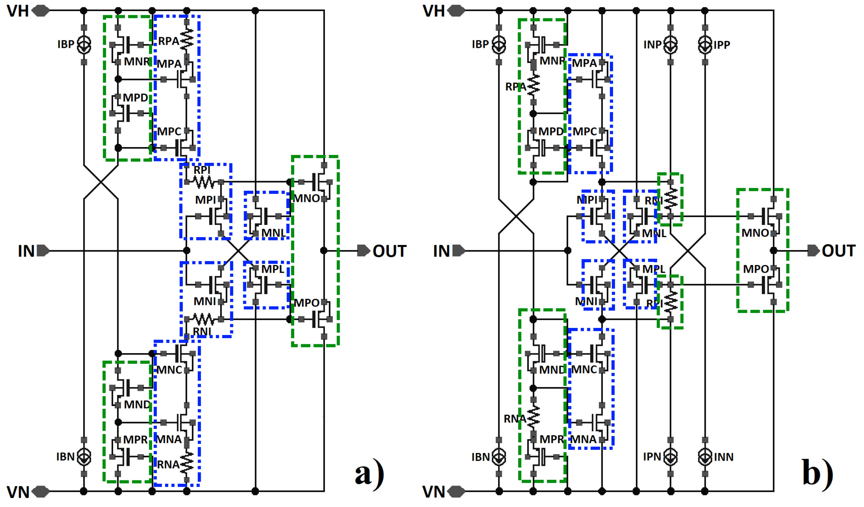
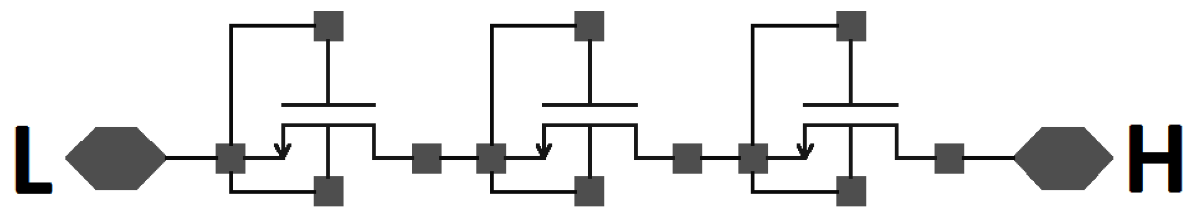
The operation principles of the scrutinized buffer are described in [1]. In short, the implemented topology may be considered as a gate follower mixed with a source follower into the new buffer topology. The simplified cores of these mentioned buffers are presented in Figure 1a–c. The goal of the buffer architecture mix is to cumulate assets of both ancestral follower types. The introduced buffer offers high input impedance typical for gate followers and fairly high precision of voltage gain, typical for source followers. The scrutinized structure can be considered a gate follower in which the biasing currents are devised with the use of structures that partially mimic the operation of the source follower input stage. The input and output stages of the source and gate followers are clearly marked in Figure 1a,b. The output stage of the gate follower is marked in the same way as the source follower because it is the same structure. The markings in Figure 1c point to all reuse cases of the input and output stages derived from the followers presented in Figure 1a,b.
The idea is to produce bias currents for the input side of a buffer in a manner that ensures good control over the gate-source and drain-source voltages of the buffer input stage transistors. Fixed bias currents flow through transistors that mimic parts of the source follower input, thus producing voltages that are used to drive the transistors that generate optimized bias currents for the input-stage transistors. These transistors mimic parts of the gate follower input stage in turn. The current-generating and input-stage transistors are all matched. Thus, the voltages between the buffer input and the gates of the output stage transistors are very similar to the gate-source voltages of the MOS transistors that mimic parts of the source follower input stage.
It can be stated that the gate-source voltages of the transistors that mimic the source follower input stage are converted to currents with the use of the gate follower input-stage mimicking transistors. These currents flow through the input stage transistors of the mixed buffer that also mimic the gate follower input stage, and thus produce the gate-source voltages identical to the voltages on the transistors that mimic the input stage of the source follower. These voltages are used to drive the output stage of the scrutinized buffer, identical to that in the source follower. It is a kind of voltage-current-voltage (C-V-C) conversion that enables the replacement of the input stage of the source follower input stage of the gate follower input stage, but with both gain precision of the source follower and high input impedance of the gate follower retained [1,9]. Figure 1c presents the simplest version of the scrutinized buffer. This version does not provide control over the drain-source voltages of the transistors involved in the C-V-C conversion process.
The buffer version presented in Figure 1d provides control over both the gate-source and drain-source voltages of these transistors. This effect is obtained by applying four cascode-like structures that are also matched with relevant transistors derived from the source or gate followers. On the other hand, this modification additionally increases the input impedance by means of a cascode-like effect due to implemented transistor interconnections.
The main asset of this approach is that the signal path of the scrutinized buffer is kept very short, and no additional feedback is applied in the buffer operation principle, which could pose some stability related problems. The bias current and signal flows are straightforward. The only dependence of operation between specific devices in this buffer is their matching. Most of the circuitry discussed is located outside the signal path and works purely under DC conditions. It is the DC domain-biasing current module and its internal interconnections that provide strict control over the voltages at the MOS transistors in the signal path.
The idea of forming the unity-gain buffer with its output stage formed like in source followers but with a modified structure of its input stage is shown in the published research. The approach mentioned above and shown in [6] is a two-stage operational amplifier (OPAMP) with an output unity gain buffer that acts as the third and final power stage of the OPAMP. The input side of this buffer is simply submerged into the second gain stage of the OPAMP and it is formed by a single resistor responsible for proper biasing of both the output power stage transistors.
Figure 2a,b presents two versions of the buffer that are equipped with sets of matched resistors [1]. The presence of these low-value resistances makes it possible to cope with the consequences of possible differences between the optimal gate-source voltages of the low-voltage and medium/high-voltage MOS devices present in the buffer. This is an important issue, as these kinds of transistors directly interact in the devised buffer. The low voltage MOS transistors are used in the design because of their superior matching precision, which results in higher precision buffer operation. MOS transistors that produce lower gate-source voltages are series connected to the auxiliary resistors. It should be noted that both of the structures with the resistor sets are the two most complex versions of the buffer. Figure 2a shows the buffer version for higher gate-source voltages of the utilized medium/high-voltage MOS transistors, and Figure 2b shows the buffer structure for the opposite case. The latter version is equipped with additional current-based resistor biasing circuitry.
The application of such auxiliary circuitry depends on the properties of low- and medium/high-voltage MOS transistors available in the technology process selected for physical implementation of the medium- and high-voltage analog processing circuitry. Also, there are processes in which only medium- or high-voltage transistors can be used in the buffer design, though with increased deterioration of the buffer operation quality (mainly related to matching issues). The circuit analyzed in this paper is the most complex version of the buffer architecture with resistor biasing circuitry (Figure 2).
2.2. The Biasing Circuitry
Figure 3, Figure 4 and Figure 5 show the complete schematics of the source follower from Figure 1a, the gate follower shown in Figure 1b, and the scrutinized buffer from Figure 1d.
It is clear that in every case the biasing circuitry constitutes a vast majority of the buffer transistor count. In contrast, the numbers of transistors in the signal paths are equal to six in the case of the scrutinized buffer and four in the case of its ancestral buffers.
To keep the current biasing process close to the quality provided by ideal current sources, cascode current mirrors are widely implemented. The main transistors of the current mirrors are always low-voltage MOS devices, while cascode transistors can be both low- and medium-voltage devices, depending on their location in the design. The medium-voltage MOS devices are used in the case of the cascode transistors, e.g., current mirror outputs exposed to high swings of the processed voltage signals. Such high voltage swings would result in drain-source and drain-gate voltages destructive to the implemented low-voltage devices.
The biasing circuitry is equipped with the enable/disable functionality to keep the biasing block off by means of redirecting the input bias current to the proper supply rail by shorting the MOS transistors of the input stages in specific bias current mirrors.
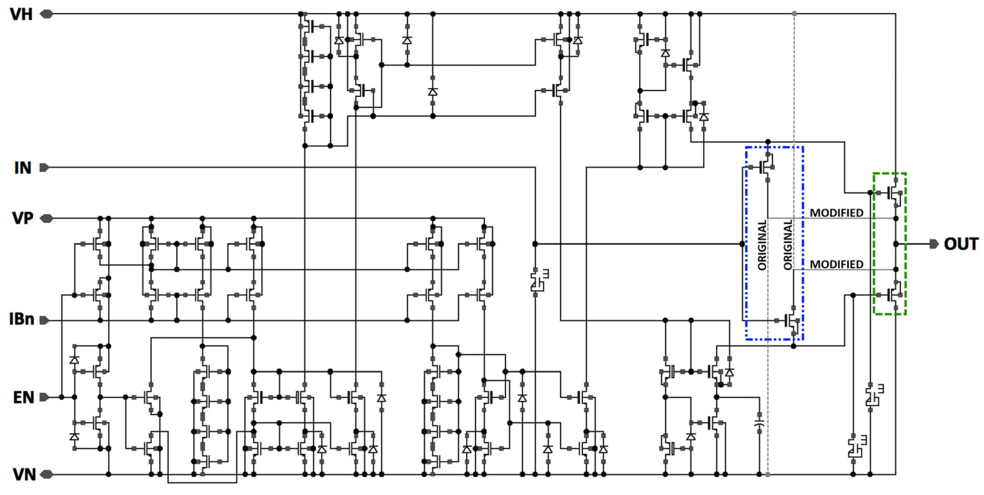
In fact, Figure 4 shows two variants of the gate follower, named ‘original’ and ‘modified’. The original is the complete schematic implementation of the buffer presented in Figure 1b. In the modified version, drains of the input transistors are redirected from the ground and supply rails to the buffer output. This is possible due to sufficient current sinking and sourcing capabilities of the low-impedance output.
This change was made as an experimental way of providing a means of control over the drain-source voltage of these transistors similar to that provided in the buffer in Figure 5 but without additional devices involved in the design.
The influence of this solution is discussed later in the paper. It is worth mentioning that there is also a version of the scrutinized mixed buffer equipped with such a modification, and it undergoes its own examination, too.
2.3. Schematic-Level Comparison of the Source, Gate, and Mixed Buffers
Other topologies of unity-gain buffers based on source-followers have also been proposed. For example, an interesting medium- to high-voltage buffer for the control of the TFT LCD panel control is proposed in [10]. In addition, an interesting series of symmetric unity gain buffers is described in [11,12,13]. These circuits are able to provide output impedance even lower than that of the circuitry dealt with in this paper, and they tend to offer rail-to-rail signal processing capabilities. However, the main objective of the scrutinized buffer is the maximization of its input impedance.
Also, the aforementioned topologies use rather complex circuits in their signal paths to obtain a very low output resistance. In contrast, the implemented buffer [1] keeps most of its circuitry introduced outside the signal path. Such an approach simultaneously keeps the signal processing path as short as possible and potentially enables various signal-path modifications to be implemented alongside the already added off-the-path biasing circuitry. For example, some of the circuit modifications presented in [10] or even in [11,12,13] might be attempted in the presented buffer, in order to extend the set of its virtues.
Another set of adaptations to the source follower architecture is voltage conveyors (VC). Two implementations of second-generation VCs are introduced in [14,15]. Again, these modifications are focused on improving different operation parameters than in the case of the buffer scrutinized in this paper. The presented conveyors adapt the source follower architecture to maximize the load driving capabilities. The end result is circuits with non-optimized input impedance and increased complexity of their signal paths.
Direct comparison of adaptations to the voltage-follower-based architecture with totally different purpose and optimization goals might result in limited conclusions related to the quality of the operation parameters critical for the scrutinized buffer. The decision was made to compare the scrutinized buffer with its ancestral source and gate followers, as it was devised to combine the best virtues of these two buffers by mixing their architectures. As mentioned before, the mixed buffer is expected to provide input impedance at least comparable to that offered by the gate follower, as well as the gain value precision (and output-input DC offset) of the source follower. Thus, it is important to compare the specified operation aspects of all these buffers to prove the efficiency of the discussed mix of these two buffer architectures.
The mentioned operation parameters of the analyzed buffer were compared with those of source and gate followers with identical sizes of the related MOS transistors. It must be noted that the physically implemented mixed buffer analyzed in this paper is created as an independent test structure inside an application-specific integrated circuit (ASIC). Its input node has an additional ESD protection, but its output stage is a robust structure capable of dealing with the parasitic capacitances of the pins of this test ASIC, as well as the ASIC package pads and utilized measurement probes. On the other hand, the unity-gain buffers can, and often are, used inside the cores of ICs, preceded and followed by other function blocks. In such circumstances, there is no need for very robust output stages. To include such an application of unity gain buffers into the comparison, modified versions of the source, gate, and mixed buffers were prepared and simulated. They are equipped with smaller transistors of their output stages. MOS devices of the output stages are twice as wide as the MOS devices used in the input stage of the source follower and their matched equivalents used in the mixed buffer.
Both sets of the source, gate, and mixed buffers were implemented at the schematic level and simulated with the Cadence Virtuoso software coupled with the Spectre simulator and the up-to-date design kit of the X-FAB XDM10 modular 1.0 μm 350 V Trench Insulated BCD (Bipolar-CMOS-DMOS) process used during the physical implementation process. The high supply voltage is set to 18 V, and the low supply voltage is equal to 5 V. All compared buffers were tested in the time domain. The input nodes were fed with 5.5 V 0-p sine waves with a 9 V DC offset (half of the high supply voltage). The outputs of the buffers were floating.
The implemented buffers consist of the MOS transistors, referred to in the paper as low-voltage and medium-voltage devices. In fact, the classification of transistors is unique for specific processes. In the case of the XDM10 process, the buffer uses ne, pe, nme, nmeb, and pme type transistors, described in [16,17]. All of them have a maximum gate source voltage (VGS) equal to 18 V, which is a rather high and very useful value of this parameter. Their formal division into low- and medium-voltage devices is based on maximum drain-source voltage (VDS). In the case of ne and pe type devices, referred to as low-voltage transistors, the maximum VDS is 5.5 V, while in the case of nme, nmeb, and pme type devices, referred to as medium-voltage transistors, it is equal 20, 32 and 20 V, respectively.
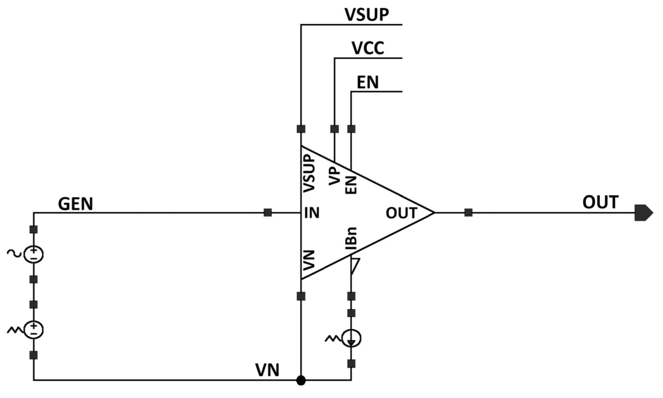
One of the problems related to the direct comparison of different published design topologies is the influence of different semiconductor processes used during the design process, as well as different device sizing. It was found by the author that his own schematic level implementations of the presented buffer architectures may provide discernibly different results when based on different semiconductor processes. To express this problem, the comparison was extended with a set of three buffers implemented at the schematic level with the use of the SMARTIS 0.8 µm BCDMOS SOI (Silicon on Insulator) process (also known as TFSMART 1) [1]. All these buffers are intended for operation inside IC cores and can be considered as equipped with small output stages. In the case of the SMARTIS-based buffers, the high supply voltage was set to 27 V and the low supply voltage to 5 V for all the discussed simulations. The input nodes of all these buffers were fed with 6 V 0-p sine waves with 13.5 V DC offsets (half of the high supply voltage). The outputs of the buffers were floating. The simulation setup is presented in Figure 6.
Table 1, Table 2 and Table 3 present the results of a time-domain comparison of the gain value, output-input DC offset shift, and input impedance of every tested buffer, respectively. The presented comparison includes four buffer architectures. The source follower is represented by the structure presented in Figure 3 and its close equivalent implemented in the SMARTIS process. The gate follower is the structure presented in Figure 4 (the original version without connection between the input- and output-stage transistors) and its SMARTIS based equivalent. The modified gate follower is the structure presented in Figure 4 (the modified variant with drains of the input stage transistors connected to the output node). The mixed buffer is the structure presented in Figure 5 and its SMARTIS-based equivalent introduced in Figure 7.
Table 1 presents the voltage gain values of the compared buffers. These gains are presented in decibels. The ideal voltage gain is equal to 1 V/V or 0 dB. Thus, the values presented can be interpreted as voltage gain errors. It can be observed that the SMARTIS based buffers offer gain values closer to the expected unity gain. It can also be seen that the relations between the gain values (errors) for the compared buffer architectures are different for the SMARTIS- and XDM10-based buffers, although these structures are close equivalents (Figure 5 and Figure 7, respectively, in the case of the mixed buffer). Comparison of the XFAB-based buffers with small and large output stages shows very similar values of the gain errors and relations between the compared buffer architectures. In the case of the gain value, the main difference results from the application of a different technology process.
Table 2 presents the output-input DC offset values of the compared buffers. The SMARTIS-based buffers offer lower values of the DC offset, with exception to the gate buffer, which has the highest DC offset of all the compared buffer variants. The mixed buffer offers the smallest DC voltage shift of all the SMARTIS-based buffers. The same result was obtained for the XDM10-based buffers. However, in the case of the latter buffers, the offset values are largest for the source followers, intermediate for the gate followers, and smallest for the mixed buffers. The modified gate buffer offers slightly (the small output variant) or significantly (the large output variant) lower offset value. The offset values for the source and mixed buffers implemented in the XDM10 process are very similar. In the case of the offset value, again it is the different implementation process that causes most of the result differences.
Table 3 presents the comparison of the input impedance magnitude values. The input resistance was calculated as a division of the root mean square (RMS) of the input voltage sine wave amplitude divided by the RMS of the resulting input current wave amplitude. This approach was adopted after checking that the input current wave may be considered as a sine wave with acceptable total harmonic distortion (THD). The smallest input impedance values were obtained for the source followers, intermediate for the classic gate followers, and the largest for the mixed buffers. In general, the SMARTIS-based buffers offer comparable or lower input impedance values. The difference is most pronounced for the mixed buffers.
The XDM10-based mixed buffers offer the highest input impedance. As pointed out before, the mixed buffer architecture was devised to provide interconnection between voltage-mode and current-mode modules in medium/high-voltage signal paths. High input impedance is critical in such applications, because input of the buffer is usually directly connected to the node that is the very point where the current-to-voltage conversion process takes place. The modified gate followers offer the input impedance values comparable (the large output stage variant) or discernably larger (the small output stage variant) than the corresponding XDM10 based mixed buffers.
In the case of the input impedance comparison, the result divergences caused by the application of different semiconductor processes are generally similar to those caused by significant output stage sizing changes in the buffers implemented in the same process (XDM10). The exception are results for the scrutinized mixed buffers, for which the result discrepancies caused by the implementation of different processes are the largest, again.
2.4. Conclusions for the Schematic-Level Comparison
In general, the conducted comparison showed that implementation of the buffers with the use of different processes provided most of the result difference between the corresponding buffer architectures.
The comparison also showed that the best set of values for the critical parameter values was provided by the scrutinized mixed buffers. The mixed buffers offer the lowest values of the output–input DC offset, voltage gain values comparable to those offered by the source followers, and input impedance values superior to both the source and gate followers, as intended.
The results worth mentioning are those obtained for the modified gate followers, presented in Figure 4. The input impedance values for these buffers are comparable or even higher than in the case of the mixed buffers. Although the DC offset values are about 50% higher and the voltage gain errors are slightly higher, the most critical parameter is the input impedance. It might be stated that the modified gate followers are enough because they provide comparable operation parameters, and their architecture is simpler (Figure 4) than in case of the mixed buffers (Figure 5). The modified gate followers are smaller and consume less power than the scrutinized mixed buffers. If true, this would be an important note, because the modified variant of the gate follower is an attempt at a kind of a ‘low cost’ improvement of the gate follower input impedance, obtained by means of MOS device reconnections with no additional devices in the design.
However, there is one aspect of the architecture that the modified gate followers lack as opposed to the mixed buffers. The presented simulations do not take either process parameter variations or device matching issues into consideration. The modified gate follower properties rely on nonrelated MOS transistors of different types (the PMOS input transistor drives the NMOS output transistor and vice versa). Such devices cannot be matched because they are manufactured during different process steps, and parameter variations of the layers that constitute these devices are generally unrelated. On the contrary, the mixed buffer architecture is completely based on matching of the related MOS transistors of the same type. Thus, this architecture is by far less prone to deterioration caused by both the variation of the process parameter variation and the limitations related to the device positioning and shape definition-related limitations.
Unfortunately, the XDM10 process models of the utilized MOS devices do not include any matching parameters, so the influence of the technology process imperfections on the buffer parameter deterioration cannot be directly simulated.
3. Physical Implementation
3.1. Introduction
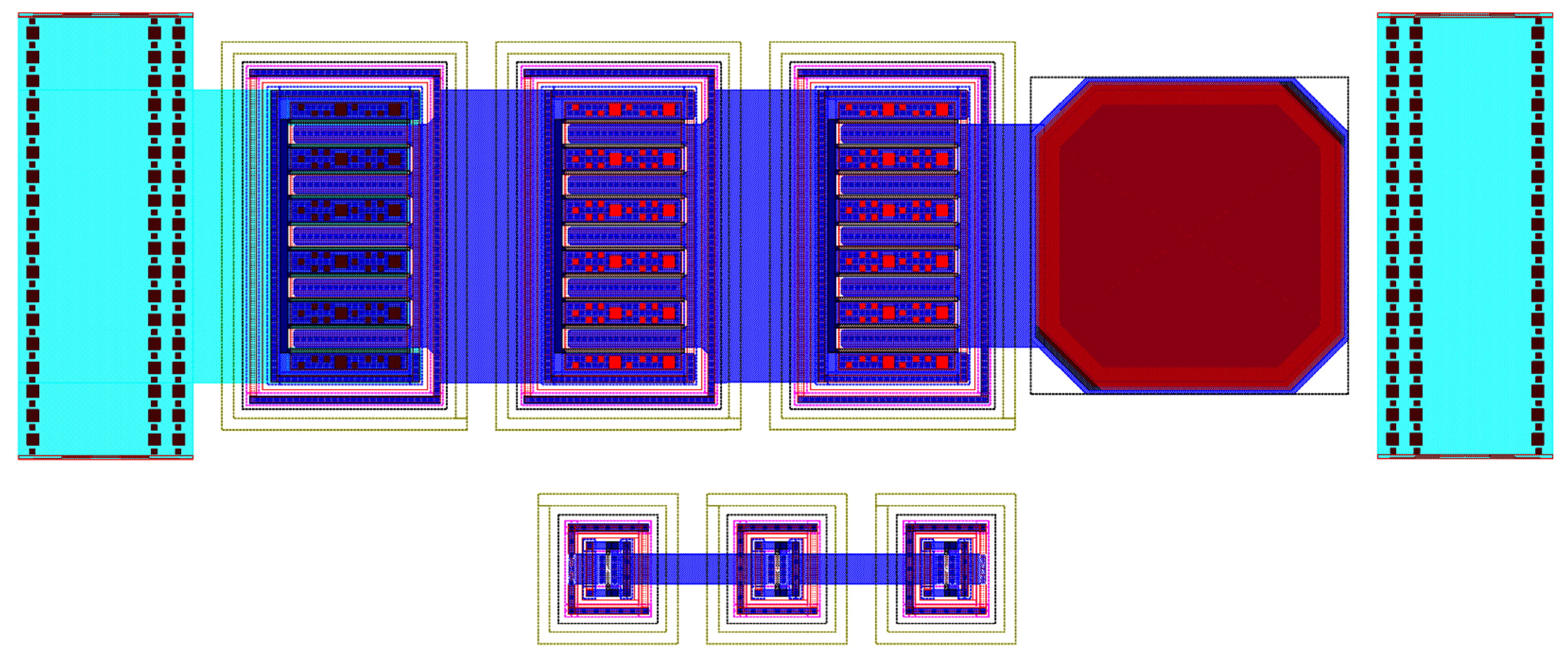
The scrutinized buffer was implemented with the use of a few thoroughly different CMOS and SOI processes. Most of these implementations ended at the schematic stage of the design process. However, two of the other implementations were endowed with a full set of overvoltage protection devices. The buffer implemented with the aforementioned SMARTIS 0.8 µm BDC-on-SOI process is depicted in Figure 7, while the buffer implemented with the AMS H35B4 0.35 µm CMOS process is presented in Figure 8.
It can be seen that these buffers were drawn using similar placement and connection styles and the similarity is easy to recognize. Differences between the specifications of the processes used during the buffer implementations result in generally different sets of safety devices.
These differences can be briefly characterized as different ratios of maximum voltages between pairs of MOS device terminals, mainly MOS transistor gate-source and drain-source voltages. None of the overprotection devices utilized are more complicated than two series sets of diodes or diode-connected MOS transistors in an antiparallel configuration.
3.2. Overvoltage and ESD Safety Devices
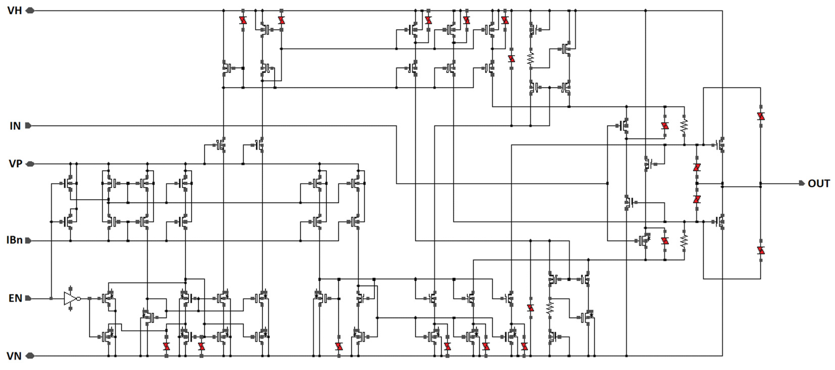
The circuit presented in Figure 5 is able to provide all required functionality under all required operating conditions. As already discussed, there are the low-voltage and high-voltage MOS device interconnections which can lead to possible excessive voltage occurrences at specific low-voltage transistors. Such incidents should be avoided, lest these low-voltage devices get damaged.
All transistors used in the buffer implementation with the X-FAB XDM10 process have 18 V maximum gate-source voltage. Application of only the medium-voltage MOS transistor could solve most of the overvoltage-related issues at once. Such an approach is possible (and has been investigated and used for tests), but it must be remembered that the precision of the buffer operation strictly depends on the matching of specific sets of its transistors. Unfortunately, the medium-voltage devices of the XDM10 process have significantly worse matching properties than the low-voltage devices. This statement is based on data presented in the process documentation documents [16]. According to [16], the matching parameters of the transistors use Pelgrom coefficients [18] where the standard deviation of the mismatch between neighboring MOS transistors is calculated vs. the square root of the channel area. The transistor matching is characterized by a set of process-related constants proportional to the standard deviation of the transistor mismatch distribution. These parameters are as follows: AVT0, Aβ, AIDx and characterize threshold, linear region gain, and drain current mismatch, respectively. The x represents the gate-source overvoltage (the difference between the gate-source and threshold voltages) for which the constant is applied. The values of the AVT0, Aβ, AIDx mismatch constants for the low-voltage MOS devices utilized (as derived from the documentation data) are lower by factors of 1.8–2.3, 1.1–2.1, and 1–4.2 (for low overvoltage), respectively. The application of as many better-matching transistors as possible provides significant benefits to operation quality [19], as the buffer operation depends on precise current mirroring and voltage-current-voltage conversions only with the use of the MOS transistors.
Due to the properties of the XDM10 process, it was possible to use floating wells even in the case of single MOS transistors, if needed. Such a possibility enabled the application of the low-voltage transistors in the buffer signal path where they must be able to withstand high-swing input signals. In effect, the low-voltage NMOS and PMOS transistors in the signal path are placed in their own wells. These transistors are matched with their related transistors in the biasing circuitry, which are also placed in separate wells.
Studies were also conducted to determine whether it would be possible to remove most or all of the medium-voltage transistors from the buffer design. This approach is known and there are analog [20] and digital [20,21] circuits that can be designed this way. Unfortunately, it was concluded that, due to details of the buffer structure and requirements for operation with reasonably fast high-swing signals, this approach cannot be used. The cascode transistors of the cascode current mirrors and the majority of the signal path transistors were found to need the medium-voltage implementations.
The voltages between each pair of MOS device terminals must be kept within safe margins for every MOS transistor in the design. Due to the properties of the utilized transistors and types of interconnections between them, it is mainly the gate-source and drain-source voltages that need to be limited.
Information about the occurrences of excessive voltages in the implemented buffer is provided by simulations with application of special device models equipped with safe operating area condition (SOAC) limits. In the case of the X-FAB processes, these models are called operating condition check (OCC) models [22] and are available for all components utilized. The functionality of the buffer was tested with frequency and time domain simulations. All details of all the simulation setups are introduced in Section 4: Buffer Operation Analysis.
The output logs of the simulations conducted with use of the OCC models provide information whether, when, and how much any voltage and current of any device in the design leaves and returns to the safe operating area of this device. Owing to this information, every such occurrence can be tracked down, analyzed, and properly amended. As a result of OCC based analyses, several safety devices were added to the original circuit (presented in Figure 5). In the simplest cases of gate-source overvoltage spikes, the application of capacitors (or capacitor-based circuits) was found enough, as applied in [23]. Most of the applied safety devices are reverse-connected p-n diodes (dn and dp types) and Zener diodes (dzeb type), as presented in Figure 5. Some of the Zener diodes act as bidirectional protection devices.
There are also three protection structures of a different kind implemented in the buffer. They act as ESD/overvoltage devices, and their presence in the design is not a result of any simulation-based analysis. It should be remembered that the input and output nodes of the implemented buffer are connected to their own input and output pads in the integrated test structure. These pads are equipped with their own ESD devices, but the safety of the externally accessible buffer nodes is critical and was further analyzed. The author discussed the raised safety issues with the X-FAB foundry engineers, and a suggestion was made to place additional local ESD/overvoltage devices directly at the buffer input and output nodes.
The schematic of these applied structures is presented in Figure 9. The transistor number and interconnections are identical for both pad-related and local ESD devices. In both cases, three nme-type MOS transistors are utilized. The layouts of these ESD devices differ discernibly. The pad ESD structures are the most critical and are laid out completely in accordance with the special ESD-optimized process rules [24,25] based on or similar to various published ESD-focused layout optimization methods for MOS transistors [26,27,28] and other devices [27,29]. The local mini structures follow the most critical of these rules. The resulting layout structures are optimized for maximum protection efficiency. Special care is required during the preparation of the ESD device layouts, as these ESD-focused rules are not included in the standard design rule check (DRC) rulesets. Figure 10 presents one of versions of both the pad-related ESD and local overvoltage structures based on the schematic presented in Figure 9, laid side by side on the same scale. A close-up of the local ESD structure is shown in Figure 11.
Fortunately, no more complex overvoltage circuitry, such as that presented in [30], was found to be necessary. On the other hand, there were no cases where overvoltage protection could have been obtained by an affordable change in a circuit structure, and without need of application of any protection-only related subcircuits, such as in the case of a high-voltage switch presented in [31].
3.3. Layout
The buffer layout was prepared on the basis of the SOAC schematic, and it includes all the safety devices. The addition of a considerable number of these safety devices increases the size of the buffer layout area, but they are necessary to ensure safe operation. Fortunately, these additions increase the layout area by less than 5%.
Apart from a standard current biasing circuitry that receives and copies the external bias current, the buffer layout contains a mix of specialized current biasing circuitry specific to the scrutinized mixed buffer as well as the signal path devices. The placement of these devices is strictly determined by the matching requirements of the buffer design and the technology process itself. Due to the need to match the transistors operating in different parts of the ground to supply voltage space and due to structural details of some of the medium-voltage transistors used in the buffer, each of these low-voltage and medium-voltage transistors is placed in its own separate well.
The requirement of placing the MOS transistors in separate wells resulted with increased spacing between the sets of transistors that should be matched in compliance with the layout preparation rules presented in [32]. Even though the transistors are not always placed in the closest vicinity of their matched counterparts, they are at a distance range that will not result in deteriorated matching properties [16,32]. In addition to matching the MOS transistors themselves, their interconnections are also kept as symmetrical as possible to increase the quality of the buffer operation [32].
As already mentioned, the implemented mixed buffer is equipped with a massive output stage. The prepared output stage transistor matrices are designed to drive measurement equipment probes connected to the test structure pads or to the external pins of test PCBs with the bare or packaged test die on board. This means that all extra parasitic capacitances connected to the buffer output must be taken into account to be properly coped with by the buffer itself. The implemented buffer is biased with an externally generated current flow. This current is generated by a dedicated function block inside the IC test structure. This block is not treated as part of the buffer structure because it also provides bias currents to several other test blocks.
4. Buffer Operation Analyses
4.1. Simulation Setup
The aim of the conducted simulations is to analyze the operation analysis of the implemented buffer and compare it with all preceding stages of its design. The general behavior and the critical operation parameters are taken into account.
Three main design advancement stages of the presented buffer are compared, along with one layout structure prepared just for comparison’s sake. First, the original buffer schematic consisting of the core and bias circuitry fed with an externally provided bias current (Figure 5, without any safety devices) is considered. Next, the SOAC buffer schematic equipped with all necessary safety devices (the buffer shown in Figure 5 with all safety devices) is taken into account. As a final design step, the layout of the SOAC buffer, is included in the comparison. The additional (and artificial) structure is the layout of the buffer without any safety devices. This layout may be considered as the layout of the original schematic. This structure has been included in the comparison to enable analysis of the differences between the original and SOAC buffers at both at the schematic and layout stages of design advancement.
The comparison is made by means of several different simulations. The physically implemented buffer versions are represented by their post-layout parameter extraction netlists. The parameter extraction process provides information on the parasitic components present in the prepared layouts. The presence of these parasitics influences the operation of the designed circuit, and this influence can be compared to the effect caused by the addition of the safety devices and to the cumulative influence of the parasitics and safety devices (with their own parasitics). Simulations of all buffer netlist variants were conducted for the XDM10 process with the use of the Cadence Vitruoso software coupled with the Spectre simulator and the relevant design-kit. An 18 V high voltage supply, 5 V low voltage supply, and 10 µA bias current power and bias the buffers during all the simulations.
The input signals are always placed symmetrically in the ground-to-high-voltage supply voltage range. The input and output buffer nodes are equipped with pad-related ESD structures identical to those designed and used during the physical implementation of the buffers (Figure 10). The simulation setup is presented in Figure 12.
4.2. AC-Domain Comparison
All frequency domain simulations were performed for the AC input signal atop the 9 V DC input offset voltage. Figure 13 presents the simulation results for the schematic and parameter extraction-based netlists of the original and SOAC versions of the scrutinized buffer. It can be clearly seen that the physical implementation of the buffer results with a visible limitation of the small-signal cutoff frequency. However, there is also a discernible reduction in this frequency for the SOAC buffer, both at the schematic and layout stages of advancement.
The implemented safety devices contain their own resistances and capacitances, both as devices inherent to their operation principle and as parasitics. It can be noticed that the differences between the original and SOAC buffer versions are significantly smaller than between the physically implemented and schematic-based buffer versions. The quantitative details of this comparison are presented in Table 4. The presented frequency-domain simulations provide a comparison of the operation speed limits of the tested buffer implementation stages. It must be remembered that frequency-domain simulations are small-signal ones, whereas the discussed buffer operates as a large-signal circuit. For a more realistic comparison of operation speed capabilities, time-domain simulations were also conducted.
4.3. Time-Domain Comparison
The SOAC-related time-domain simulations of the power-up, operation, and shut-down phases of the buffer work were conducted with the following setup. The simulation starts with all the supply voltages, the bias current, and the input voltage equal to zero and the enable signal low. After two microseconds, the high and low voltages and the bias current start to ramp up from 0 to their nominal values (18 V, 5 V, and 10 µA, respectively) and finish this process in 2 µs, while the enable signal remains low. After reaching the nominal values of the supply voltages and the bias current, the enable signal remains low for another 2 µs. The enable signal is used to redirect the input bias current so that it bypasses the input bias current mirror and flows directly to the ground node (Figure 5). Next, the enable signal changes to high in 10 ns. This signal redirects the input bias current so that it enters the input current mirror (Figure 5).
After another 2 µs the input signal changes from 0 to half of the high supply voltage value. After another 2 µs the input signal changes to the sine wave. Depending on the tested operation parameter, its amplitude varies from 5 V 0-p amplitude to the ground-to-high-supply voltage range. After several tens of microseconds, the procedure is inverted. The input signal is changed to a DC value and then goes to the ground, the enable signal goes low, and then the high and low supply voltages as well as the bias current are ramped down to the ground level. The simulation is finished when the buffer is discharged and the voltages and currents of all the observed terminals are zero.
Simulations of input impedance, voltage gain, and DC offset were conducted with the use of the test-bench presented in Figure 6.
Figure 14 presents the results of one of such simulations. All buffer versions are driven with input signals defined as 5.5 V 0-p amplitude sine waves atop the 9 V offset voltage to keep these signals in the middle of the rail-to-rail voltage range. The 21 MHz frequency is selected so that the output signal of the original buffer schematic version is reduced by nearly 3 dB, indicating the large-signal cutoff frequency of the original buffer schematic.
First, it can be observed that time-domain simulations can provide more detailed information on the buffer operation quality for high input signal frequencies. All the output waveforms presented in Figure 14 are noticeably distorted in the same way. These simulations were conducted for the floating buffer output to exclude effects related to the pad-related ESD circuitry. Generally, it can be seen that the buffer is not well suited for large-signal operation close to its cutoff frequency. The amplitudes of the output waveforms for all the tested stages of the buffer design progression confirm the results of the comparison in the AC domain. The addition of safety devices only slightly slows down the operation of the SOAC buffer versions, which can be observed as a reduction in the output waveform magnitudes.
The laid-out buffers represented by their post-layout parameter extraction-based netlists show significantly lower speed capabilities than their schematic-based counterparts. The same consistent trends can be seen for 3 dB cutoff frequency values of all the compared buffer variants. Quantitative results are presented in Table 4.
Time simulations can also be useful for checking the operation of buffer versions for lower input waveform frequencies. Figure 15 presents the time-domain curves of differences between the output and input sinusoidal waveforms at 100 kHz. The waveforms for schematics of the original and the SOAC buffer versions are nearly identical (46.43 mV magnitude for the 11 V input waveform). The output-input voltage shift amplitude for both of the laid-out buffers is equal to about 61 mV and 31% higher than in the case of the schematic-based versions.
These results show that the addition of safety devices barely alters this aspect of the buffer operation at the selected signal frequency. The shape of the curves presented in Figure 15 points to a low level of the output waveform distortions. The output–input curves are almost of sinusoidal shape, which means that the main difference between the output waveforms and purely sinusoidal input waveforms is the time shift between these waveforms.
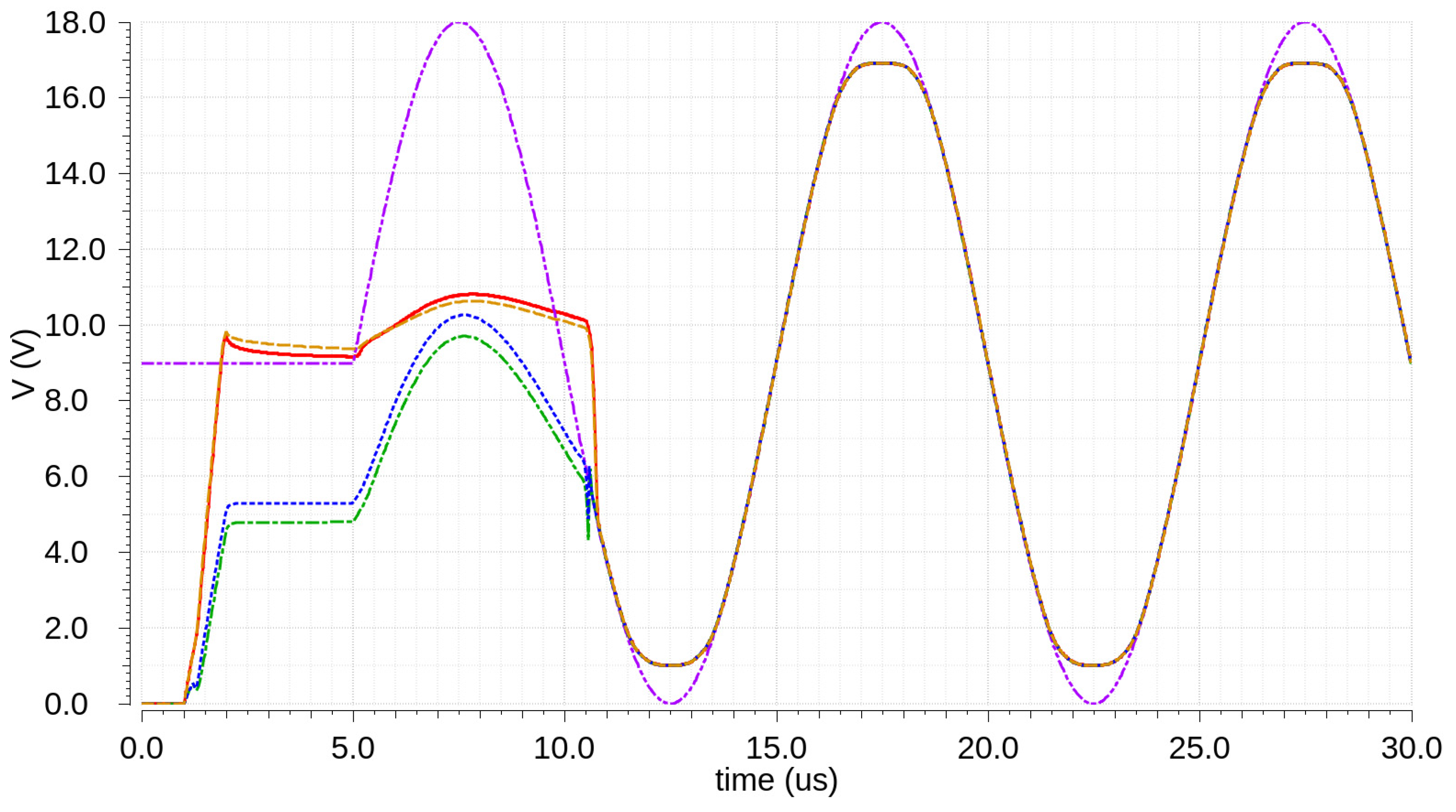
Additionally, the maximum voltage ranges of the output waveforms have been checked for all four variants of buffer implementation. Figure 16 presents the 100 kHz input sinusoidal waveform and the resulting output signals during the rapid power-up sequence and normal operation. It can be seen that the analyzed buffer does not offer a rail-to-rail input signal processing range. However, there is no visible difference between the output signal voltage ranges for different variants of the scrutinized buffer.
Figure 16 also shows how different the output voltage of the buffer variants can be during the power-up sequence, depending on the buffer variant. However, it can be seen again that most of the differences are present between the schematic- and layout-based buffer netlists. The difference between the original and SOAC buffers is significantly lower for both the schematic- and layout-based buffer netlists.
4.4. Noise Simulations
An important factor in the operation of an electronic circuit is noise influence. This aspect was also examined for the buffer discussed. According to the process documentation [33] all the transistors used in the buffer are equipped with noise-related parameters, despite the fact of modelling low-voltage transistors with different models than medium-voltage devices. The implemented noise modelling is limited to 1/f noise, but this is not a major issue. The presented buffer can be considered a low-frequency circuit, and the 1/f noise is pronounced and important in that frequency range [34].
Figure 17 presents the results of the AC domain output noise simulations of all buffer variants. The AC input signal is placed on top of the 9 V DC offset. Again, the results for both of the laid-out buffers show very similar results. Also, results of both of the schematic-based variants of the buffer show a very similar noise level, about 5–12 dB higher than in the case of the laid-out buffers, in the pass frequency range of these buffers. In the range of the large-signal cutoff frequency of the buffers (10 MHz), this difference is about 5–5.5 dB (Table 5).
A factor that might limit the precision of the noise-related simulations is the absence of noise modelling for diodes used as safety devices. Most of the safety diodes are placed outside the signal path. There are only two of them in the signal path of the buffer, while there are three safety devices, each based on three stacked MOS transistors, and these devices are clearly the largest safety devices in the whole buffer. The decision was taken to conduct AC and transient noise simulations to further analyze the operation parameters of all four examined buffer implementation stages.
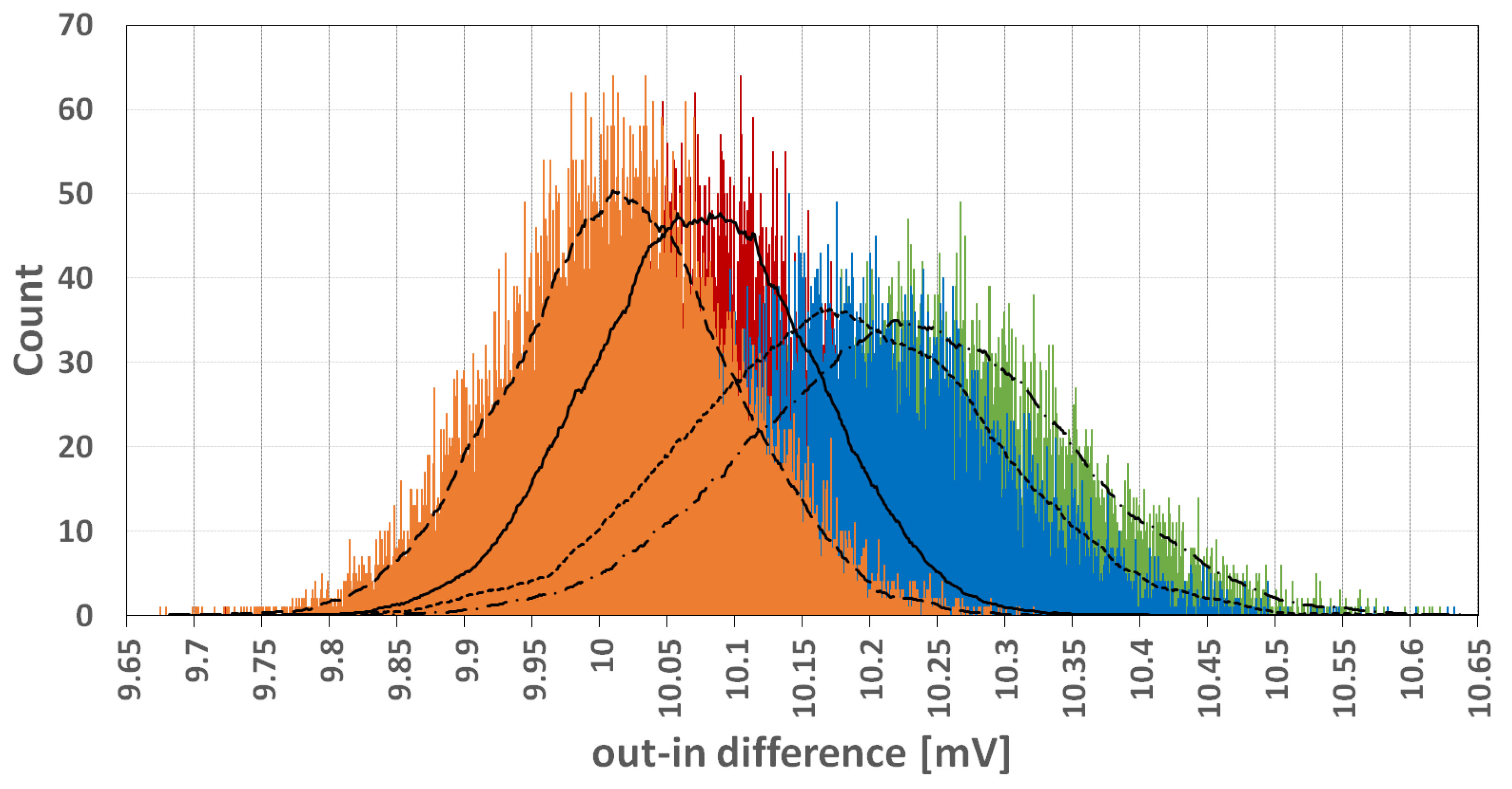
The time domain SOAC simulations of the output noise were performed for all variants of the buffer. The input signal is the 9 V DC voltage, and the noise is presented as a distribution of 10,000 samples of the output signal, including the mean value and standard deviation. Figure 18 shows the readout distribution for the layout-based simulation of the SOAC variant of the buffer (with safety devices). The shape of the distribution is symmetric and bell-shaped, which points to no obvious problems, neither with the circuit operation nor the simulation setup.
Figure 19 presents readout distributions with their envelopes for all the scrutinized variants of the buffer. The readout distributions of the laid-out buffers are very similar to each other. The same conclusion is true for the schematic-based buffers. The standard deviation values for pairs of the laid-out and schematic-based variants of the buffer are almost identical, as shown in Table 5, while the standard deviation difference for the laid-out and schematic-based buffers is about 40%. The differences between the mean values within such pairs of the buffers are bigger, but still three times lower than that between the buffers from opposite pairs (laid-out vs. schematic-based), as presented in Table 5.
4.5. Discussion of the Results
All comparisons made show that the influence of the entire set of safety devices is very limited. According to the simulations discussed and their results shown in Figure 13, Figure 14, Figure 15, Figure 16, Figure 17, Figure 18 and Figure 19 and Table 4 and Table 5, the results are consistent for all the simulations in the frequency and time-domain simulations. The parameter value differences between the schematic-based buffers and, separately, between the pair of laid-out buffers are significantly lower than between the corresponding schematic-based and laid-out buffer variants.
Of course, the simulations performed cannot take into account all aspects of buffer operation. For example, noise is modeled only for the utilized MOS devices and only as 1/f noise. However, the conducted simulation analyses provide an important degree of insight into the influence of the necessary internal safety devices on the buffer operation. The limited influence of the implemented safety devices can be attributed to the fact that the buffer signal path is kept very short and most of these safety devices are placed outside (in the biasing subcircuitry), as shown in Figure 5.
The process of laying out the buffer causes a much more pronounced deterioration of the buffer operation parameters, which is a typical outcome of the physical implementation process. Such a deterioration can be coped with during the earlier stages of the circuit design through the preparation of schematics with operating parameter margins expendable during the laying process. Additional and significantly smaller deterioration of the buffer operation related to the application of the safety devices can be easily dealt with precisely in the same way, if necessary.
Comparison of the results obtained with other works is rather difficult. Analog circuits are generally very diverse. Therefore, a possible comparison could not necessarily be made to a close functional counterpart of the discussed buffer and implemented with the use of a similar technologic process. Though, the main problem found by the author is the impression that the influence of implemented internal safety/overprotection circuits on the operation on IC function blocks seems to be seldom analyzed or at least presented. On the other hand, publications on the influence of pad-related ESD structures on internal circuit operation (mainly speed issues) can be found for both analog [35] and digital [36] integrated components.
5. Comparison of the Source, Gate, and Mixed Buffers for All Tested Stages of the Physical Implementation Progress
5.1. Simulation Results of the Scrutinized Buffer
All the DC offset, voltage gain, and input impedance values obtained for the physically implemented SOAC buffer are generally different from those obtained in the schematic-based comparison presented in Section 2.3. Unfortunately, the most pronounced difference is the input impedance of the completely implemented SOAC buffer (Table 4). Input impedance reductions between the schematic- and layout-based variants of the scrutinized buffer are about 65 times for the original versions and 38 times for the SOAC buffer versions. The input impedance limitation between the original and the SOAC versions of the buffer is about 2.1 times in the case of the schematic stage of buffer design and is virtually absent in the case of the laid-out buffers.
The design step that causes most of the deterioration of this parameter is the laying of the buffer. This remark is consistent with a general conclusion made for the physical implementation process. Nonetheless, the significant reduction of the critical operation parameter of the designed buffer requires more attention. It should be checked if the parameter deterioration is a design-specific issue or rather a general problem of physical implementation, at least in the selected semiconductor process.
5.2. Comparison of the Critical Operation Parameter Changes
In order to follow this issue, another simulation-based comparison was performed. The critical operation parameters were checked for the source, gate, and mixed buffers at all four designed stages taken into account so far. Simulation setup is identical as in the case of the simulations related to the schematic-based comparison of the scrutinized buffer with its ancestral architectures (Figure 6). The results of the voltage gain, DC offset, and input impedance comparison are presented in Table 6, Table 7 and Table 8, respectively.
As presented in Table 6, the voltage gain values for all four compared buffer architectures are only slightly (less than 20%) deteriorated throughout the design stages from the original schematic to the SOAC layout.
A similar conclusion can be drawn for the DC offset comparison (as presented in Table 7). The deterioration of this parameter is less than 20% in the most pronounced cases.
The input impedance comparison (Table 8) shows a major deterioration for all the simulated buffers. The most pronounced effects can be observed in the case of the buffers intended to provide the highest quality of their operation. It can be seen that the reduction to the input impedance between the original schematic and the SOAC layout in the case of the source, classic/modified gate, and mixed buffers is equal to 2.9, 7.7, 50.58 and 61.51 times, respectively.
The highest and similar input resistance reduction ratios are present for the modified gate buffer and for the scrutinized mixed buffer. The basic source and gate followers have input impedance reduction ratios much closer to each other than to any of the more advanced architectures. This is an important outcome, because the modifications to the signal path of the modified gate and mixed followers are expected to provide the same result. In both cases, the drains of the input-stage transistors are connected in ways that largely limit variation of the drain-source voltages of these transistors.
In the case of the modified gate buffers, the input stage transistor drains are connected to the output node, and in the case of the mixed buffer, they are connected to the sources of the auxiliary transistors. It is worth mentioning that the more complex scrutinized buffer with a higher number of transistors in its signal path and more sophisticated biasing circuitry results with only slightly (about 20%) more pronounced input impedance reduction in comparison to the modified gate follower with its simpler signal path design and basic biasing circuitry.
Although the SOAC layout of the modified gate follower offers its input impedance higher by 12.7%, it must be remembered that this design is much more prone to process parameter variation and device matching precision issues, as mentioned in Section 2.3.
5.3. Discussion of the Comparison Results
The final conclusion of the performed comparison is that the process of laying the scrutinized buffer out caused a pronounced reduction of its input impedance being the critical operating parameter. In addition, this effect is present in all the compared buffer structures. This effect increases with the internal complexity of the tested buffers, but the scrutinized buffer still provides the highest value of input impedance among the buffers that employ cooperation and matching of devices of the same type to ensure their proper operation. The input impedance of the scrutinized mixed buffer is more than 12.8 times higher than that of the source follower. An issue for future research would be to investigate whether such an input impedance reduction after the physical implementation of the compared buffers is mostly connected to the properties of the semiconductor process or to the internal architecture of the implemented buffers, in general. It is a problem worth solving, as the architecture of all the compared buffers, including the scrutinized mixed buffer, is intentionally kept as simple and short as possible. Most of the added circuit complexity is placed outside of the signal path in the DC operating bias circuits.
6. Conclusions
The author analyzed and discussed the influence of the design advancement of the analyzed high-input impedance buffer on its structure details and operation parameters. The issue was investigated due to the necessity of applying about 30 overvoltage protection devices in order to ensure save operation of the buffer during its power-up, normal-operation, and power-down phases. The presence of these additional safety devices is necessary because of commonly implemented interconnections of the utilized low-voltage and medium-voltage MOS transistors with significantly different maximum interterminal voltages, due to the superior matching properties of the low-voltage MOS transistors. The safety devices include a capacitor, p-n diodes, Zener diodes and stacks of diode-connected MOS transistors. The conducted analyses include frequency- and time-domain simulations of the circuit operation, along with frequency- and time-domain noise influence analysis.
The analyses performed by the author show that the addition of all these devices of several different types causes only minor deterioration in the signal processing quality of the scrutinized buffer. It is the physical implementation process that was found to be the main source of deterioration to the buffer parameters. Operation parameters like the voltage range of properly processed input signals, voltage gain error, and output–input DC offset remain generally unchanged throughout the entire design process advancement from the schematic of the original buffer to the final layout of the SOAC buffer. Among the main limitations caused by the laying process, there are chiefly those related to the operating speed limits.
Unfortunately, the author also found that one of the seriously affected parameters of the scrutinized buffer is its input impedance. The problem is that the analyzed buffer was designed with the very goal of obtaining an increased value for this parameter. Thus, such a result required further analysis. A comparison was performed to analyze the deterioration of the critical operation parameters for the scrutinized mixed buffer and its ancestral source and gate followers. The author found that the detected parameter deterioration is a common phenomenon in all the compared buffer structures. It is more pronounced for more complex structures in general, and not particularly so in the case of the scrutinized buffer. The commonness and degree of the deterioration of speed and input impedance deterioration found by the author for the scrutinized and all the compared buffers suggests the necessity of a comparative analysis against physical implementations with the use of different medium- and high-voltage technology processes. It is worth mentioning that all the buffers taken into account have extremely short signal paths with a very limited number of devices between their inputs and outputs. Also, the ancestral buffers of the scrutinized mixed buffer are rather typical and well-known source and gate follower structures.
The author presented a specific approach to circuit operation analysis in relation to the application of internal devices that serve purely safety/overvoltage roles. In the course of the performed studies, the author found this approach not to be a common one. It is not clear whether it is caused by the limited influence of typically applied safety devices or if stress is placed on the analysis of single stages of the circuit design, like final layouts of designed circuits, only. The presented analyses provide information on deterioration of the operation quality of the scrutinized buffers. The results gathered and analyzed by the author show that the process of equipping the buffers with sets of required safety devices is of secondary importance to their operation quality. On the other hand, it is still the physical implementation process that was found to be the source of major changes to the circuit operation parameters, even in the case of rather simple and typical buffers.
The outcome of the analyses performed by the author might be found useful and informative for designers of middle- or high-voltage analog integrated circuits, starting from the stage of technology process selection.
Funding
This research was supported by the Department of Microelectronics and Computer Science of the Lodz University of Technology.
Institutional Review Board Statement
Not applicable.
Informed Consent Statement
Not applicable.
Data Availability Statement
Data are contained within the article.
Acknowledgments
The author expresses his gratitude to Andrzej Napieralski, the Head of the Department of Microelectronics and Computer Science of the Lodz University of Technology, for the decision to fund the manufacturing of an ASIC consisting, e.g., the buffer presented in this paper, which was essential for the continuation and completion of the whole design process.
Conflicts of Interest
The author declares no conflict of interest.
References
- Jankowski, M.; Napieralski, A. High-voltage high input impedance unity-gain voltage buffer. Microelectron. J. 2013, 44, 576–585. [Google Scholar] [CrossRef]
- Jankowski, M.; Napieralski, A. Current-mode signal processing implementation in HV SoI integrated systems. Microelectron. J. 2014, 45, 946–959. [Google Scholar] [CrossRef]
- Jankowski, M.; Napieralski, A. Novel Structure of CMOS Voltage-to-Current Converter for High Voltage Applications. In Proceedings of the NANOTECH Conference & Expo 2012, Santa Clara, CA, USA, 18–21 June 2012. [Google Scholar]
- Jankowski, M. Improvements of High-voltage Trapezoidal Waveform Edge-rounding Circuit. Int. J. Mi-Croelectron. Comput. Sci. 2018, 9, 93–100. [Google Scholar]
- Xu, L.; Li, H.; Li, P.; Ge, C. The Application of Classical Control in the Design and Analysis of Power Amplifiers for Driving Piezoelectric Stack Actuators. Electronics 2021, 10, 720. [Google Scholar] [CrossRef]
- Xu, L.; Li, H.; Li, P.; Ge, C. A High-Voltage and Low-Noise Power Amplifier for Driving Piezoelectric Stack Actuators. Sensors 2020, 20, 6528. [Google Scholar] [CrossRef] [PubMed]
- Bhuiyan, M.A.S.; Badal, T.I.; Reaz, M.B.I.; Crespo, M.L.; Cicuttin, A. Design Architectures of the CMOS Power Amplifier for 2.4 GHz ISM Band Applications: An Overview. Electronics 2019, 8, 477. [Google Scholar] [CrossRef] [Green Version]
- Merenda, M.; Iero, D.; Della Corte, F.G. CMOS RF Transmitters with On-Chip Antenna for Passive RFID and IoT Nodes. Electronics 2019, 8, 1448. [Google Scholar] [CrossRef] [Green Version]
- Jankowski, M. Implementation of a Modified High-Voltage Unity-Gain Buffer. In Proceedings of the 28th International Conference on Mixed Design of Integrated Circuits and Systems, Lodz, Poland, 24–26 June 2021; pp. 110–114. [Google Scholar] [CrossRef]
- Park, S.-Y.; Son, S.H.; Chung, W.S. A rail-to-rail unity gain buffer amplifier for low-cost high resolution TFT LCD panels. IEEE Trans. Consum. Electron. 2009, 55, 2190–2194. [Google Scholar] [CrossRef]
- Wongfoo, F.; Naklo, W.; Suadet, A.; Kasemsuwan, V. A Simple Rail-to-Rail CMOS Voltage Follower. In Proceedings of the TENCON 2006—2006 IEEE Region 10 Conference, Hong Kong, China, 14–17 November 2006; pp. 1–4. [Google Scholar] [CrossRef]
- Boonyaporn, P.; Kasemsuwan, V. A high performance class AB CMOS rail to rail voltage follower. In Proceedings of the IEEE Asia-Pacific Conference on ASIC, Taipei, Taiwan, 6–8 August 2002; pp. 161–163. [Google Scholar] [CrossRef]
- Sawigun, C.; Demosthenous, A.; Liu, X.; Serdijn, W.A. A Compact Rail-to-Rail Class-AB CMOS Buffer with Slew-Rate Enhancement. IEEE Trans. Circuits Syst. II Express Briefs 2012, 59, 486–490. [Google Scholar] [CrossRef]
- Barile, G.; Stornelli, V.; Ferri, G.; Safari, L.; D’Amico, E. A New Rail-to-Rail Second Generation Voltage Conveyor. Electronics 2019, 8, 1292. [Google Scholar] [CrossRef] [Green Version]
- Safari, L.; Barile, G.; Stornelli, V.; Minaei, S.; Ferri, G. Towards Realization of a Low-Voltage Class-AB VCII with High Current Drive Capability. Electronics 2021, 10, 2303. [Google Scholar] [CrossRef]
- X-FAB Semiconductor Foundries. Process Specification XDM10—1.0 μm Modular DIMOS 350Vs. Unpublished work. 2014. [Google Scholar]
- X-FAB Semiconductor Foundries. Design Rule Specification XDM10—1.0 μm Modular DIMOS 350V. Unpublished work. 2014. [Google Scholar]
- Pelgrom, M.; Duinmaijer, A.; Welbers, A. Matching properties of MOS transistors. IEEE J. Solid-State Circuits 1989, 24, 1433–1439. [Google Scholar] [CrossRef]
- Cheng, Y. The influence and modeling of process variation and device mismatch for analog/rf circuit design. In Proceedings of the Fourth IEEE International Caracas Conference on Devices, Circuits and Systems (Cat. No.02TH8611), Oranjestad, The Netherlands, 19 April 2002; p. D046. [Google Scholar] [CrossRef]
- Serneels, B.; Steyaert, M. High Voltage Implementations in Standard CMOS. In Design of High Voltage xDSL Line Drivers in Standard CMOS; Analog Circuits and Signal Processing Series; Springer: Berlin/Heidelberg, Germany, 2008. [Google Scholar] [CrossRef]
- Chow, H.-C.; Chen, Y.-G. A reliable and high voltage compatible CMOS I/O buffer. In Proceedings of the 2004 47th Midwest Symposium on Circuits and Systems, 2004, MWSCAS ’04, Hiroshima, Japan, 25–28 July 2004; p. iii-451. [Google Scholar] [CrossRef]
- X-FAB Semiconductor Foundries. Application Note—SPICE Models & Simulations. Unpublished work. 2016. [Google Scholar]
- Aboadla, E.; Khan, S.; Kadir, K.; Yusof, Z.; Habaebi, M.; Habib, S.; Islam, M.; Hasan, M.; Hossain, E. Suppressing Voltage Spikes of MOSFET in H-Bridge Inverter Circuit. Electronics 2021, 10, 390. [Google Scholar] [CrossRef]
- X-FAB Semiconductor Foundries. XDM10/XDH10 NMOS/PMOS ESD Protection Device and Latch-up Guidelines. Unpublished work. 2009. [Google Scholar]
- X-FAB Semiconductor Foundries. XDM10/XDH10 TLP I-V Characteristics. Unpublished work. 2009. [Google Scholar]
- Fan, S.-K.; Chen, S.-L.; Lin, P.-L.; Chen, H.-W. Layout Strengthening the ESD Performance for High-Voltage N-Channel Lateral Diffused MOSFETs. Electronics 2020, 9, 718. [Google Scholar] [CrossRef]
- Keppens, B.; Mergens, M.P.; Trinh, C.S.; Russ, C.C.; Van Camp, B.; Verhaege, K.G. ESD protection solutions for high voltage technologies. Microelectron. Reliab. 2006, 46, 677–688. [Google Scholar] [CrossRef]
- Ker, M.-D.; Chang, W.-J. Overview on ESD protection design for mixed-voltage I/O interfaces with high-voltage-tolerant power-rail ESD clamp circuits in low-voltage thin-oxide CMOS technology. Microelectron. Reliab. 2006, 47, 27–35. [Google Scholar] [CrossRef]
- Hong, S.-Z.; Chen, S.-L. ESD Design and Analysis by Drain Electrode-Embedded Horizontal Schottky Elements for HV nLDMOSs. Electronics 2021, 10, 178. [Google Scholar] [CrossRef]
- Zimmermann, N.; Wunderlich, R.; Heinen, S. An over-voltage protection circuit for CMOS power amplifiers. In Proceedings of the 15th IEEE International Conference on Electronics, Circuits and Systems, ICECS 2008, St. Julien’s, Malta, 31 August–3 September 2008; pp. 161–164. [Google Scholar] [CrossRef]
- Osipov, D.; Paul, S. A novel HV-switch scheme with gate-source overvoltage protection for bidirectional neural interfaces. In Proceedings of the 2015 IEEE International Conference on Electronics, Circuits, and Systems (ICECS), Cairo, Egypt, 6–9 December 2015; pp. 25–28. [Google Scholar] [CrossRef]
- X-FAB Semiconductor Foundries. Design Guidelines for Improved Device Matching. Unpublished work. 2009. [Google Scholar]
- X-FAB Semiconductor Foundries. GSA Mixed-Signal/RF SPICE Model Checklist. Unpublished work. 2012. [Google Scholar]
- Teramoto, A. Evaluation of Low-Frequency Noise in MOSFETs Used as a Key Component in Semiconductor Memory Devices. Electronics 2021, 10, 1759. [Google Scholar] [CrossRef]
- Feng, H.; Gong, K.; Wang, A.Z. A comparison study of ESD protection for RFICs: Performance vs. parasitics. In Proceedings of the 2000 IEEE Radio Frequency Integrated Circuits (RFIC) Symposium Digest of Papers (Cat. No.00CH37096), Boston, MA, USA, 11–13 June 2000; pp. 235–238. [Google Scholar] [CrossRef]
- Ungru, T.; Wilkening, W.; Negra, R. Influence of ESD on an integrated shift register in operation. In Proceedings of the 2017 11th International Workshop on the Electromagnetic Compatibility of Integrated Circuits (EMCCompo), Saint Petersburg, Russia, 4–8 July 2017; pp. 136–140. [Google Scholar] [CrossRef]
Figure 1.
Symmetrical buffers: (a) gate follower; (b) source follower; (c) modified basic modified buffer; (d) augmented buffer [1].
Figure 1.
Symmetrical buffers: (a) gate follower; (b) source follower; (c) modified basic modified buffer; (d) augmented buffer [1].

Figure 2.
Two versions of the buffer equipped with sets of small resistors: (a) for higher gate source voltages of medium/high-voltage MOS transistors; (b) for the opposite case [1].
Figure 2.
Two versions of the buffer equipped with sets of small resistors: (a) for higher gate source voltages of medium/high-voltage MOS transistors; (b) for the opposite case [1].

Figure 3.
Complete schematic of the source follower.

Figure 4.
Complete schematic of the gate follower.

Figure 5.
Complete schematic of the scrutinized buffer [9].
Figure 5.
Complete schematic of the scrutinized buffer [9].

Figure 6.
Simulation setup for the schematic-based buffer comparison.

Figure 7.
The buffer implemented with the ATMEL SMARTIS 0.8 µm BDC-on-SOI process.

Figure 8.
The buffer implemented with the AMS H35B4 0.35 µm CMOS process.

Figure 9.
Schematic of an ESD/overvoltage device used on the input and output side of the buffer.

Figure 10.
Pad-related ESD and local overvoltage structures based on the schematic presented in Figure 9 laid side by side on the same scale.
Figure 10.
Pad-related ESD and local overvoltage structures based on the schematic presented in Figure 9 laid side by side on the same scale.

Figure 11.
A close-up of the local ESD structure shown in Figure 10.
Figure 11.
A close-up of the local ESD structure shown in Figure 10.

Figure 12.
Simulation setup for comparison of the buffer implementation stages.

Figure 13.
Frequency-domain comparison of the buffer implementation stages: the original buffer—blue dotted line; the SOAC buffer-green dashed-dotted line; the laid-out original buffer—orange dashed line; the laid-out SOAC buffer-red solid line.
Figure 13.
Frequency-domain comparison of the buffer implementation stages: the original buffer—blue dotted line; the SOAC buffer-green dashed-dotted line; the laid-out original buffer—orange dashed line; the laid-out SOAC buffer-red solid line.

Figure 14.
Time-domain comparison of the buffer design stages for input 21 MHz, 5.5 V 0-p amplitude (violet dash-dash-dotted line): the original buffer—blue dotted line; the SOAC buffer—green dashed-dotted line; the laid-out original buffer—orange dashed line; the laid-out SOAC buffer—red solid line.

Figure 15.
Time-domain curves of differences between the output and input sinusoidal waveforms at 100 kHz: the original buffer—blue dotted line; the SOAC buffer—green dashed-dotted line; the laid-out original buffer—orange dashed line; the laid-out SOAC buffer—red solid line.
Figure 15.
Time-domain curves of differences between the output and input sinusoidal waveforms at 100 kHz: the original buffer—blue dotted line; the SOAC buffer—green dashed-dotted line; the laid-out original buffer—orange dashed line; the laid-out SOAC buffer—red solid line.

Figure 16.
100 kHz input sinusoidal waveform (violet dash-dash-dotted line) and comparison of the resulting output signals during the power-up sequence and normal operation; the original buffer—blue dotted line; the SOAC buffer—green dashed-dotted line; the laid-out original buffer—orange dashed line; the laid-out SOAC buffer—red solid line.

Figure 17.
Results of the AC domain output noise simulations of all buffer variants; the original buffer—blue dotted line; the SOAC buffer-green dashed-dotted line; the laid-out original buffer—orange dashed line; the laid-out SOAC buffer-red solid line.
Figure 17.
Results of the AC domain output noise simulations of all buffer variants; the original buffer—blue dotted line; the SOAC buffer-green dashed-dotted line; the laid-out original buffer—orange dashed line; the laid-out SOAC buffer-red solid line.

Figure 18.
Readout distribution for the layout-based simulation of the SOAC variant of the buffer (with safety devices).
Figure 18.
Readout distribution for the layout-based simulation of the SOAC variant of the buffer (with safety devices).

Figure 19.
Readout distributions for all the scrutinized variants of the buffer with their envelopes; the original buffer—blue and dotted line; the SOAC buffer—green and dashed-dotted line; the laid-out original buffer—orange and dashed line; the laid-out SOAC buffer—red and solid line.
Figure 19.
Readout distributions for all the scrutinized variants of the buffer with their envelopes; the original buffer—blue and dotted line; the SOAC buffer—green and dashed-dotted line; the laid-out original buffer—orange and dashed line; the laid-out SOAC buffer—red and solid line.


Table 1.
Comparison of voltage gain [dB (V/V)] for different schematic stage implementations of the source follower, gate followers and the discussed buffers.
Table 1.
Comparison of voltage gain [dB (V/V)] for different schematic stage implementations of the source follower, gate followers and the discussed buffers.
| Buffer Version | Source Follower | Gate Follower | Improved Gate Follower | The Discussed Buffer |
|---|---|---|---|---|
| SMARTIS small output | −10.2 m | −16.8 m | - | −7.3 m |
| XDM10 small output | −29.80 m | −48.98 m | −28.52 m | −35.57 m |
| XDM10 large output | −30.82 m | −49.13 m | −28.94 m | −38.67 m |
Table 2.
Comparison of output–input DC offset [V] for different schematic stage implementations of the source follower, gate followers, and discussed buffers.
Table 2.
Comparison of output–input DC offset [V] for different schematic stage implementations of the source follower, gate followers, and discussed buffers.
| Buffer Version | Source Follower | Gate Follower | Improved Gate Follower | The Discussed Buffer |
|---|---|---|---|---|
| SMARTIS small output | −7.5 m | −123.4 m | - | −6.0 m |
| XDM10 small output | −36.63 m | −29.04 m | −28.57 m | −9.755 m |
| XDM10 large output | −35.99 m | −28.51 m | −20.23 m | −10,20 m |
Table 3.
Input impedance [MΩ] comparison for different schematic stage implementations of the source follower, gate followers, and discussed buffers.
Table 3.
Input impedance [MΩ] comparison for different schematic stage implementations of the source follower, gate followers, and discussed buffers.
| Buffer Version | Source Follower | Gate Follower | Improved Gate Follower | The Discussed Buffer |
|---|---|---|---|---|
| SMARTIS small output | 0.73 | 17.0 | - | 73.0 |
| XDM10 small output | 1.473 | 15.05 | 342.9 | 272.7 |
| XDM10 large output | 0.5876 | 15.0 | 148.4 | 160.1 |
Table 4.
Comparison of the buffer properties for all the selected implementation stages.
| The Buffer Variant | Small-Signal Cutoff Freq. [MHz] | Large-Signal Cutoff Freq. [MHz] | Voltage Gain 21 MHz Sine [dB] | Out-in p-p Ripple [mV] | Out-in Difference [mV] | Voltage Gain 1 MHz Sine [V/V] | Input Z1 MHz Sine [MΩ] |
|---|---|---|---|---|---|---|---|
| The original schematic | 502.0 | 20.7 | −3.10 | 46.25 | −181.82 | 0.9956 | 160.1 |
| The SOAC schematic | 448.8 | 19.8 | −3.49 | 46.44 | −181.79 | 0.9956 | 75.78 |
| The unprotected layout | 168.8 | 4.7 | −17.09 | 60.79 | −187.40 | 0.9948 | 2.603 |
| The SOAC layout | 152.1 | 4.6 | −17.66 | 61.32 | −186.87 | 0.9948 | 2.603 |
Table 5.
Comparison of the buffer noise properties for the selected implementation stages.
| The Buffer Variant | AC Noise 106–107 Hz [V/Sqrt(Hz)] | Out-in Mean 10,000 smp [mV] | O-I Std. Dev. 10,000 smp [mV] |
|---|---|---|---|
| The original schematic | −181.82 | 10.15 | 0.1116 |
| The SOAC schematic | −181.79 | 10.20 | 0.1157 |
| The unprotected layout | −187.40 | 10.00 | 0.0825 |
| The SOAC layout | −186.87 | 10.05 | 0.0822 |
Table 6.
Comparison of voltage gain [dB] for different implementation stages of the source follower, gate followers, and discussed buffers.
Table 6.
Comparison of voltage gain [dB] for different implementation stages of the source follower, gate followers, and discussed buffers.
| Buffer Version | Source Follower | Gate Follower | Improved Gate Follower | The Discussed Buffer |
|---|---|---|---|---|
| The original schematic | −30.82 m | −49.13 m | −28.94 m | −38.67 m |
| The SOAC schematic | −30.88 m | −49.28 m | −29.68 m | −38.42 m |
| The unprotected layout | −34.69 m | −51.05 m | −29.88 m | −45,42 m |
| The SOAC layout | −35.15 m | −51.44 m | −30.13 m | −45.42 m |
Table 7.
Comparison of output to input DC offset [mV] comparison for different implementation stages of the source follower, gate followers, and discussed buffers.
Table 7.
Comparison of output to input DC offset [mV] comparison for different implementation stages of the source follower, gate followers, and discussed buffers.
| Buffer Version | Source Follower | Gate Follower | Modified Gate Follower | The Discussed Buffer |
|---|---|---|---|---|
| The original schematic | −36.30 | 28.51 | 20.23 | 10.20 |
| The SOAC schematic | −35.99 | 28.20 | 19.89 | 10.27 |
| The unprotected layout | −34.92 | 30.38 | 21.98 | 12.66 |
| The SOAC layout | −34.49 | 30.16 | 21.85 | 12.66 |
Table 8.
Comparison of input impedance [MΩ] for different implementation stages of the source follower, gate followers, and discussed buffers.
Table 8.
Comparison of input impedance [MΩ] for different implementation stages of the source follower, gate followers, and discussed buffers.
| Buffer Version | Source Follower | Gate Follower | Modified Gate Follower | The Discussed Buffer |
|---|---|---|---|---|
| The original schematic | 0.5876 | 15.0 | 148.4 | 160.1 |
| The SOAC schematic | 0.5801 | 12.95 | 75.32 | 75.78 |
| The unprotected layout | 0.2131 | 2.244 | 3.551 | 2.603 |
| The SOAC layout | 0.2027 | 1.941 | 2.934 | 2.603 |
Publisher’s Note: MDPI stays neutral with regard to jurisdictional claims in published maps and institutional affiliations. |
© 2021 by the author. Licensee MDPI, Basel, Switzerland. This article is an open access article distributed under the terms and conditions of the Creative Commons Attribution (CC BY) license (https://creativecommons.org/licenses/by/4.0/).
Share and Cite
MDPI and ACS Style
Jankowski, M. Influence of Modifications Related to Safe Operating Area Demands on Operation of a Specialized Medium/High-Voltage Unity-Gain Buffer. Energies 2022, 15, 23. https://doi.org/10.3390/en15010023
AMA Style
Jankowski M. Influence of Modifications Related to Safe Operating Area Demands on Operation of a Specialized Medium/High-Voltage Unity-Gain Buffer. Energies. 2022; 15(1):23. https://doi.org/10.3390/en15010023
Chicago/Turabian StyleJankowski, Mariusz. 2022. "Influence of Modifications Related to Safe Operating Area Demands on Operation of a Specialized Medium/High-Voltage Unity-Gain Buffer" Energies 15, no. 1: 23. https://doi.org/10.3390/en15010023
Note that from the first issue of 2016, this journal uses article numbers instead of page numbers. See further details here.