
Compact Modelling of Electrical, Optical and Thermal Properties of Multi-Colour Power LEDs Operating on a Common PCB


Department of Marine Electronics, Faculty of Electrical Engineering, Gdynia Maritime University, Morska 83, 81-225 Gdynia, Poland
*
Author to whom correspondence should be addressed.
Energies 2021, 14(5), 1286; https://doi.org/10.3390/en14051286
Submission received: 11 January 2021
/
Revised: 17 February 2021
/
Accepted: 22 February 2021
/
Published: 26 February 2021
(This article belongs to the Special Issue Selected Papers from 27th International Conference on Mixed Design of Integrated Circuits and Systems – MIXDES 2020)
Abstract
:This paper concerns the problem of modelling electrical, thermal and optical properties of multi-colour power light-emitting diodes (LEDs) situated on a common PCB (Printed Circuit Board). A new form of electro-thermo-optical model of such power LEDs is proposed in the form of a subcircuit for SPICE (Simulation Program with Integrated Circuits Emphasis). With the use of this model, the currents and voltages of the considered devices, their junction temperature and selected radiometric parameters can be calculated, taking into account self-heating phenomena in each LED and mutual thermal couplings between each pair of the considered devices. The form of the formulated model is described, and a manner of parameter estimation is also proposed. The correctness and usefulness of the proposed model are verified experimentally for six power LEDs emitting light of different colours and mounted on an experimental PCB prepared by the producer of the investigated devices. Verification was performed for the investigated diodes operating alone and together. Good agreement between the results of measurements and computations was obtained. It was also proved that the main thermal and optical parameters of the investigated LEDs depend on a dominant wavelength of the emitted light.
1. Introduction
Light-emitting diodes (LEDs) are the most important components of solid-state lighting sources commonly used in the lighting technique [1,2,3,4]. The typical application of power LEDs emitting white light is to illuminate working places and living rooms [2,3,4]. On the other hand, power LEDs emitting colour light are typically used for the illumination of buildings, bridges or other architectural objects [3,4]. Such LEDs are also used as elements of the decorative backlight at home or in hotels and restaurants. An important application of colour power LEDs is in traffic lights [4]. All the mentioned groups of power LEDs are also used in the automotive industry.
Many papers describe different scientific problems connected with the manufacturing, testing, modelling and technical applications of power LEDs [5,6,7,8]. In the last 10 years, the maximum value of the emitted luminous flux and the value of luminous efficiency have visibly increased [3,9,10]. Additionally, the price of power LEDs keeps decreasing every year. Therefore, solid-state lighting sources are more and more frequently used.
The influence of the device junction temperature on the optical and electrical properties of the power LEDs is very important [11,12,13]. An increase in the device junction temperature considerably shortens the lifetime of the considered devices [14,15,16]. A very important problem is also the thermal management of components of solid-state lighting sources. An increase in the diode temperature equal to 20 °C can cause even a sixfold decrease in its lifetime [14]. Therefore, limitation of the value of the device junction temperature and effective cooling of this device are essential. The ability to remove the heat dissipated in the considered device can be hampered by thermal resistance [17,18], which is equal to the quotient of the difference between the device’s internal temperature Tj and ambient temperature Ta per power dissipated in this device. In the JEDEC (Joint Electron Device Engineering Council) standards [19,20] and in the application notes given by the manufacturer [21], thermal resistance Rth or electric thermal resistance Rthe of power LEDs is defined. In the definition of Rth, thermal power pth equal to the difference between the electrical power (the product of diode current and voltage) and the optical power (power of the emitted light) is used. In contrast, in the definition of Rthe, the thermal power and the electrical power are equal to each other.
As stated in [22], from the point of view of the designer, accurate prediction of the junction temperature of power LEDs is very important. It makes it possible to obtain stability of lighting parameters and long lifetimes of solid-state light sources. Therefore, the design and thermal management of the considered light sources require effective and accurate thermal models [23,24]. Moreover, solid-state light sources often contain LED modules consisting of many power LEDs mounted on the same substrate. Therefore, thermal models of these devices have to take into account both self-heating phenomena and mutual thermal couplings [25]. A review of compact thermal models of semiconductor devices is presented, e.g., in [26]. The problem of formulation of such thermal models has been considered for multi-chip modules previously [27,28]. For instance, in [28], the method of thermal analysis of semiconductor devices including many heat sources is described. According to this method, the matrix of self- and transfer transient thermal impedances can be used.
While designing any electronic system, e.g., solid-state lighting systems, computer simulations are indispensable. In such simulations, proper models of all the components contained in the analysed system are needed [29]. For power LEDs, mutual interactions between electrical, optical and thermal phenomena are very important [11,28,30,31,32]. Therefore, models of power LEDs belong to the group of multi-domain models [11,30,31,32], which take into account electrical, optical and thermal phenomena occurring in such class of semiconductor devices.
Many studies [30,31,32,33,34,35,36,37] have been devoted to modelling the properties of power LEDs emitting white light, but only some studies [38,39,40] have been devoted to the problem of modelling colour power LEDs. The study in [31] focuses on power LEDs used in display systems, whereas the study in [39] considers the thermal properties of such devices. In turn, the study in [40] describes an effective procedure of measuring the characteristics of power LEDs. Studies [11,31,32] have also described the multi-domain compact models of power LEDs on the basis of an idea similar to the one presented in [30,36]. The differences between the considered models are connected with the details in the formulas describing particular parts of these models.
The study in [31] presents a fully implementable compact model of power LEDs. This model is implemented in the SPICE program. To determine the parameters of the proposed model, it is necessary to use the expensive measurement instruments described in JEDEC standards [19,20].
In [32], a new approach to the multi-domain modelling of large LED lamps, including tens of single LEDs, is presented. The compact thermal model of the whole lamp is formulated based on computational fluid dynamics (CFD) models. Thermal analyses prepared in such a way and their results can be applied in the network analogue representing the thermal model with the use of the Cauer network. Next, the parameters existing in this network are estimated and entered into the multi-domain model of the LED lamp. Unfortunately, the manner of formulating the considered model is difficult and the results of measurements and computations are presented for the steady state only.
The study in [33] contains equations describing the dependence of luminous efficiency and luminous flux on the junction temperature and the electrical power dissipated in the diode. It is shown how to estimate the diode’s forward current at which the emitted luminous flux has the maximum value.
The study in [34] presents the theory and a photo-electro-thermal model of phosphor-coated LEDs. In [41], a general 3D photo-electro-thermal LED model is described. This model accurately predicts the temperature distribution, luminous flux and correlated colour temperature (CCT) of an LED lighting system. In [42], some results of computations performed with a model from [34] are compared to the results of dynamic measurements. The dynamic version of the model from [33] is described in [43].
In [44], an analysis of the properties of white-light-emitting diodes with a large surface area was performed. These devices include a multiple-chip LED emitting blue light and a phosphor layer. The temperature distribution in the LED chip was computed, taking into account optical and thermal properties of the white phosphor coating.
In [30], a compact electro-thermo-optical model of power LEDs emitting white light is described. This is an improved version of the model presented in [35], describing a manner of estimating optical parameters in detail. The versions of the considered model presented in the mentioned papers are based on the classical Shockley model of a p-n junction given, e.g., in [39], and they describe the electrical characteristics of these devices. The thermal properties of the modelled diode are characterised by the use of one device junction temperature, the value of which depends on ambient temperature and the dissipated heating power. This power is equal to the difference between the electrical power supplying this device and the optical power characterising the emitted light. In the cited papers, the mutual thermal couplings of the modelled diode with the other diodes are omitted. The optical properties of the whole LED are characterised by luminous flux emitted by the tested LEDs. Due to the mutual interactions between the device junction temperature and the optical power, some problems with the convergence of computations performed with the use of the considered models could be observed.
In some studies [45,46], an experimental study of thermal and optical parameters of a selected LED module and thermal couplings between the diodes placed on the common base has been presented. The aforementioned LED module consists of only a dozen serially connected white power LEDs. The experimental results are compared to the results of computations. The formulated model, taking into account the three-dimensional temperature distribution, is investigated using CFD methods. This 3D model also takes into account a different heat-sink construction and different air flow rates. The prepared model also takes into account the influence of the Peltier cell temperature on the thermal and optical parameters of the investigated LED module.
In the mentioned papers, different models of power LEDs are described, but there is a lack of an electro-thermo-optical model of power LEDs emitting light of different colours. Many of these models do not take into account differences in the junction temperature of the power LED situated on a common PCB [36,47]. The study in [36] describes a model of an LED lamp containing an LED module emitting white light. In the cited model, one internal temperature characterises the thermal properties of the whole module. Meanwhile, in [48], including the results of measurements only, it is shown that due to the mutual thermal couplings between such diodes, the junction temperature of each of them can increase even by 40 °C and the differences between the values of this temperature for the diodes mounted on a common PCB can exceed even 60 °C.
This paper presents the manner of modelling the electrical, optical and thermal properties of colour and white power LEDs situated on a common PCB. The authors propose a new compact electro-thermo-optical model of such power LEDs. This model is described by the same equations as those describing the considered properties of colour and white power LEDs. The new model takes into account simultaneously self-heating in each LED and mutual thermal coupling between each pair of the considered devices. In this model, a very simple manner of computing the device junction temperature of each diode is proposed. It is based on the concept of self- and transfer electrical transient thermal impedances, which makes it possible to perform fast and accurate computations and take into account the differences in the junction temperatures of the power LEDs situated on a common PCB. The correctness of the proposed model is verified experimentally for an evaluation kit performed by OSRAM Semiconductor in cooperation with Infineon Technologies. This kit includes six power LEDs emitting light of different spectra and mounted in the same kind of cases. The investigated diodes are produced by OSRAM Semiconductor.
2. Model Form
The proposed electro-thermo-optical model of multi-colour power LEDs situated on a common PCB is based on the model of power LEDs emitting white light and described in [30]. The manner of modelling thermal phenomena is based on the concept described in [35]. According to this concept, to formulate the model of a semiconductor device, the following steps are needed:
- (a)
- Establishing some analytical equations
- (b)
- Analysing whether no redundancy between the elements occurs
- (c)
- Presenting the properties of a typical data set
- (d)
- Explaining how the data processing eliminates the outliers
- (e)
- Presenting the results set
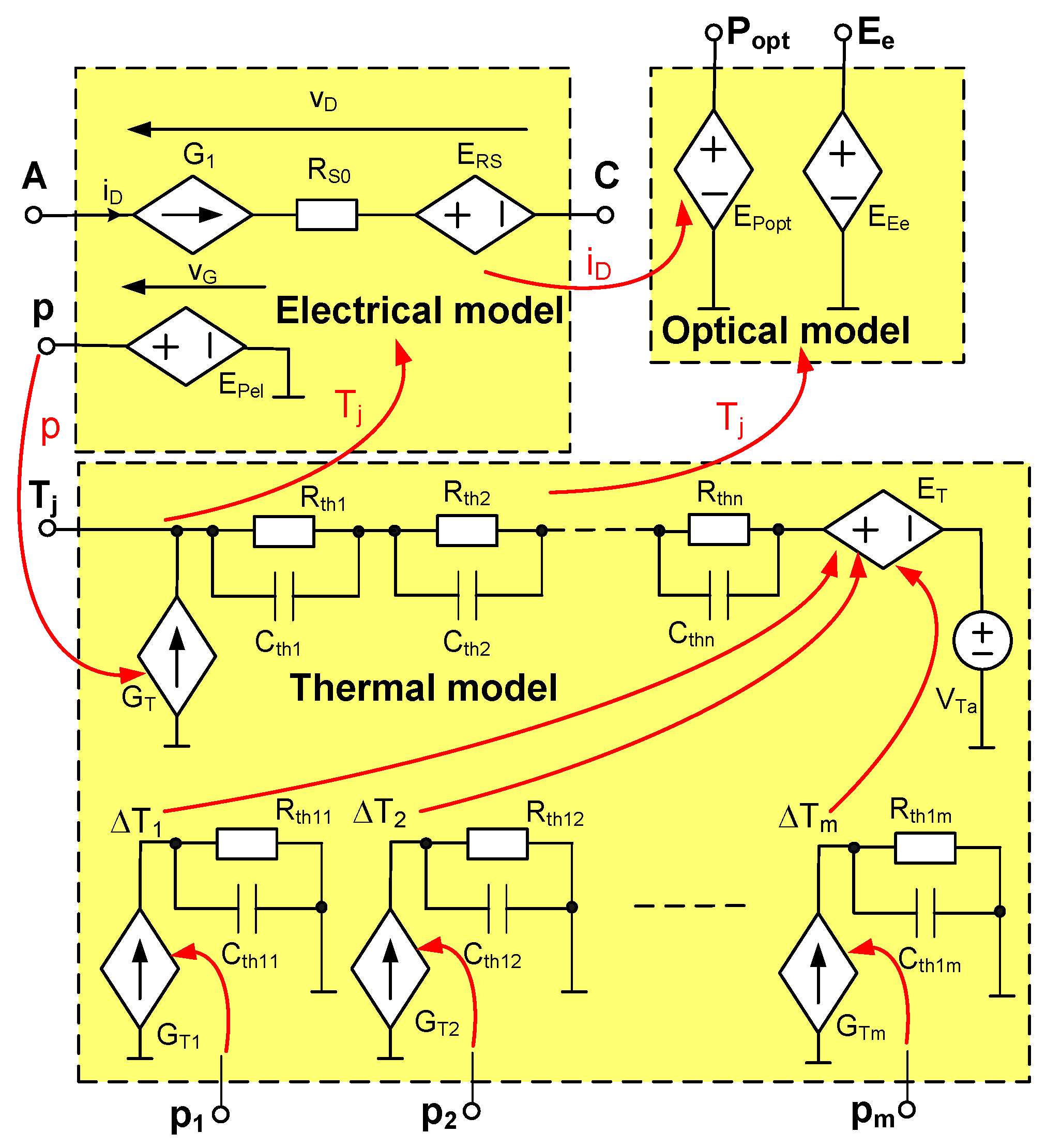
For each diode, this model is dedicated for SPICE, and it has the form of a subcircuit, the diagram of which is shown in Figure 1. In the computations, the PSPICE version 17.2-2016 was used.
This model contains three blocks: an electrical model, an optical model and a thermal model. The current–voltage characteristics of the considered devices are described in the electrical model. It takes into account the influence of the device junction temperature Tj. In the thermal model, the value of Tj is computed, taking into account self-heating phenomena and mutual thermal couplings with the other diodes situated on the same PCB. In the optical model, the surface power density of the illuminated surface and the optical power are computed, taking into account the values of the diode’s forward current iD and the junction temperature Tj. In contrast to the models of power LEDs described in the literature, in the new model, optical parameters do not influence the device junction temperature, which is computed using the idea of electrical transient thermal impedance.
The terminals A and C represent the anode and the cathode of the modelled device, respectively. Using these terminals, the considered model can be connected to the other components occurring in the application circuit of this diode. The other terminals of the model (Tj, Popt, Ee, p, p1, p2, …, pm) do not correspond to the physical terminals of the power LED, and they are used to give information about the values of optical (Popt, Ee) and thermal (Tj) quantities of the modelled device and the electrical power dissipated in the modelled diode (p) and in the other diodes situated on the same PCB (p1, p2, … pm).
In the following sections, the three above-mentioned components of the new model are described.
2.1. Electrical Model
The electrical model has a simpler form than the corresponding part existing in the photo-electro-thermal model of power LEDs emitting white light and described in [30,36]. It contains a controlled current source G1, a resistor RS0 and a controlled voltage source ERS. The source G1 models the diode current with the formula
In Equation (1), k is the Boltzmann constant; q is the electron charge; Vgo is the voltage corresponding to the band-gap energy depending on the semiconductor material used to construct the LED; vG is the voltage on the source G1; n is the emission coefficient of the diode current; and I0 is a model parameter depending on the semiconductor material, on the doping profile of the p-n junction and on the area of this junction.
As shown, e.g., in [49], the value of Vgo depends on temperature, but in the range of temperature changes from 300 to 500 K, the dependence Vgo(Tj) can be effectively modelled with the use of a linear function and the slope of this function is very low. This means that in the considered range of changes in the device’s internal temperature, Equation (1) can properly model the dependence iD(vG) in the considered range of this temperature.
Resistor RS0 is the diode series resistance at the reference temperature T0. voltage source ERS describes the linear dependence of the diode series resistance on the device junction temperature using the following formula [30]:
where αRS denotes the temperature coefficient of series resistance.
As power LEDs operate typically in forward mode only, the detailed description of the characteristics in reverse mode is neglected.
The controlled voltage source EPel is used to compute the electrical power dissipated in the modelled device. The output voltage of this source is described by the formula
The current iD and voltage vD are marked in Figure 1.
2.2. Optical Model
The optical quantities, e.g., optical power Popt and surface power density Ee, of the emitted light at a distance r from the diode are computed in the optical model with the use of the controlled voltage sources EPopt and EEe, respectively. These quantities depend both on the diode current computed in the electrical model and on the junction temperature Tj computed in the thermal model.
The surface power density of the illuminated surface Εe is described by the following formula:
In Equation (4), Ee0 denotes the surface power density of the emitted light measured at a known distance r from the tested LED in the axis of this device at the maximum value of forward current and temperature Tj equal to temperature T0. The parameters αL, αLT and αLT2 characterise the dependence of Ee on the diode’s forward current and junction temperature.
In Equation (4), a polynomial of the second degree of the junction temperature is used. Such a degree of this polynomial is selected after calculating values of the Bayesian information criterion (BIC) [50], which is the smallest for this degree of the considered polynomial.
The parameter Εe characterises the optical properties of power LEDs only in the axis of these devices. To characterise the whole light emitted by the power LED, the optical power Popt should be used. The mentioned parameter depends on the emission characteristics of the considered semiconductor device. These characteristics can be effectively approximated with the square function of the angle α between the axis of the diode and the direction of the observation. The relative surface power density of optical radiation, αopt, is described by the following formula [30]:
where a, b and c are the coefficients of the approximation polynomial.
The optical power Popt is given by the formula
where αmax denotes the emission angle at which the surface power density is equal to zero. The form of Equation (6) is obtained after the transformation of the formulas given in [30]. These formulas describe the optical power of the light emitted inside the sphere sector characterised by an emission angle. The value of Ee is measured at a distance r from the investigated diode.
2.3. Thermal Model
The compact thermal model makes it possible to compute the junction temperature Tj of the considered LED and takes into account self-heating phenomena in this device and mutual thermal couplings between the considered device and the other LEDs situated on the common PCB. As shown, e.g., in [51], in a semiconductor die, non-uniform temperature distribution is observed, whereas in the compact thermal model, only one junction temperature is used. Therefore, this junction temperature is equal to the average value of the temperature observed in this die.
The waveform of the junction temperature can be described with the following formula:
where Ta is the ambient temperature; p(v) is the electrical power dissipated in the modelled diode; pi(v) is the electrical power dissipated in diode Di, situated on the common PCB with the modelled diode; and Z′the(t) is a time derivative of self-electrical transient thermal impedance of the modelled diode, whereas Z′thei(t) is a time derivative of the transfer electrical transient thermal impedance between the modelled diode and diode Di. For each diode, one self-electrical transient thermal impedance Zthe(t) characterising self-heating phenomena and five electric transfer thermal impedances characterising the mutual thermal couplings between the modelled diode and the other diodes situated on the common PCB are used.
The parameter Zthei(t) is defined with the use of the following equation:
where Tj(t) is the waveform of the device junction temperature obtained, while the power supply of the diode Di has the form of a jump of a value equal to the product of the current iDi and voltage vDi of this diode.
As is visible after analysing the form of Equations (7) and (8), the emitted optical power does not influence the device junction temperature.
In the proposed model, electro-thermal analogy [26,52,53] is used. Therefore, the thermal model has a network form containing a few Foster RC networks. One of these networks (visible on top of the diagram of the thermal model in Figure 1) models self-heating phenomena. In this network, the controlled current source GT represents the electrical power pth dissipated in the considered power LED. Components Rth1, Rth2, …, Rthn and Cth1, Cth2, …, Cthn model self-electrical transient thermal impedance between the junction of this diode and the surroundings. The voltage source VTa represents ambient temperature. The controlled voltage source ET represents an increase in the device junction temperature caused by mutual thermal couplings between the investigated diode and the other diodes situated on the common PCB.
The terminals p1, p2 and pm are connected to the outputs p of the electrical models of the other diodes situated on the same PCB. Voltages on these terminals control the output currents of the controlled current sources GT1, GT2, …, GTm, respectively.
The output voltage of the source, ET, is equal to the sum of the voltages in nodes ΔT1, ΔT2, …, ΔTm. The voltage in each of these nodes represents an increase in the junction temperature of the tested diode caused by the electrical power dissipation in one of the other diodes mounted on the common PCB, e.g., ΔT1 by the power dissipated in the first diode and ΔT2 by the power dissipated in the second diode. Each RC network connected to the mentioned controlled current sources represents transfer electric transient thermal impedance between the investigated LED and each of the other LEDs situated on the common PCB.
The values of the parameters of RC elements describing transfer electric transient thermal impedance depend on the distance between the modelled power LED and the proper diode situated on the common PCB. In the authors’ previous investigations on diodes situated at the same distance, the same waveforms of transfer transient thermal impedance were obtained [48]. In such a case, the number of subcircuits shown at the bottom of Figure 1 can be reduced.
3. Model Parameters Estimation
A practical application of the formulated model needs estimation of the values of the parameters occurring in this model for the investigated devices. The used manner of estimating the parameters is based on the idea of local estimation presented in [36,54]. Estimation of the parameters describing the electrical properties of the modelled semiconductor devices is realised using the isothermal characteristics of these devices (obtained at the quasi-ideal cooling conditions). Such characteristics are measured with the use of the impulse method and are given in the catalogue data [54].
A manner of estimating the values that occur in the electrical model was described in [26]. In this method, electrical characteristics of the LED computed for the forward mode are used with the formulas from [36]. In the case of the considered colour power LEDs, it is very important to estimate correctly the band-gap voltage Vgo, which depends on the material used to produce these semiconductor devices. According to the considerations presented in [36], the value of this parameter can be obtained using the measured calibration curve vD(T), which indicates the dependence of forward voltage on temperature at a fixed value of forward current.
In turn, optical parameter values are estimated using the emission characteristics and measurements of the surface power density of the illuminated surface. The mentioned characteristics were approximated by means of the square function. Next, the values of the coefficients a, b and c occurring in Equation (5) are obtained using Excel software.
A manner of estimating the parameters Ee0, αL, αLT and αLT2 relating to the optical properties of the modelled devices uses the measured dependence of the surface power density of the emitted light on the diode current and the temperature. The mentioned measurements must be performed at a fixed distance r between the surface of the tested diode and the probe of the radiometer.
The values of thermal parameters, describing the electric transient thermal impedance of the tested LED and transfer transient thermal impedances between this LED and each of the other LEDs situated on the common PCB, can be estimated with the use of the ESTYM algorithm described in [26]. This algorithm uses a similar idea of parameter estimation, as described in [55]. The waveforms of self- and transfer transient thermal impedances Zthe(t) measured with the use of the method described in [12,20] are the input data for ESTYM software [37]. This software allows computing the values of parameters Rthe, N, ai and τthi describing the considered electric transient thermal impedances with the formula [18,26]
where N is the number of thermal time constants τthi corresponding to the coefficients ai of the sum equal to 1.
The value of Rthe is equal to the average value of the waveform Zthe(t) in the steady state. The values of parameters ai and τthi are computed with the use of the least-squares method. Next, values of elements Rthi and Cthi existing in the thermal model are computed with the use of the formulas given in [26].
It is worth noticing that the parameters characterising mutual thermal couplings between each pair of the diodes mounted on the same PCB could have different values, depending on the direction of the heat flow [28]. This phenomenon is a result of different values of the efficiency of conversion of electrical energy into light for LEDs emitting light of different colours.
A very important problem is analysis of the error of the parameter value estimation. This error depends on the uncertainty of measurements, the results of which are the input data for the estimation procedure. For example, the value of the surface power density of the emitted light, Ee, is measured directly with the use of a radiometer. According to the producer data [56], the measurement uncertainty does not exceed 6%. We also performed a series of measurements of the surface power density of the emitted light for selected values of the forward current of one of the investigated LEDs. The standard deviation of the obtained results normalised to the average value of the measured results did not exceed 0.35%.
In turn, transient thermal impedances occurring in the described model are measured indirectly. The manner of calculating the measurement standard uncertainty of Zth(t) using the total differential method is described in [57,58]. According to the considerations presented in the cited papers, this uncertainty depends on the type B uncertainty of the measured calibration curve, on the error of the measurements of the dissipated power and on the error of measurements of the thermo-sensitive parameter. This uncertainty is a decreasing function of the difference between the device’s internal temperature Tj and ambient temperature Ta. With properly selected instruments and a high value of the difference Tj–Ta, this uncertainty does not exceed a few percentage points.
4. Investigated Devices
For the investigations, power LEDs of the type Golden DRAGON®, manufactured by OSRAM Semiconductor (Munich, Germany) were selected. These LEDs are dedicated for use in planes and cars [59]. They emit light of six different colours: LW (white), LB (blue), LT (green), LR (red), LY (yellow) and LCW (warm white). According to the catalogue data, diodes LCW, LB, LT and LW are made of gallium nitride (GaN), whereas diodes LY and LR are made of aluminium gallium indium phosphide (InGaAlP) [59].
According to the diode datasheets [59], the maximal forward current of the investigated devices is equal to 1 A and the viewing angle amounts to 120°. The junction temperature of these diodes cannot exceed 135 °C. The values of the total luminous flux ΦV, the thermal resistance Rthj-s between the junction and the soldering point for the investigated devices and the central wavelength of the emitted light, λmax, are given in Table 1. As is visible, the total luminous flux changes in a wide range—from 15 lm for an LB diode to 130 lm for an LW diode. It is worth observing for each of the considered devices that at the same value of forward current, the luminous flux can change even twofold due to technological dispersion. The thermal resistance of these diodes between the junction and the soldering point is in the range from 5 to 6.5 K/W [59].
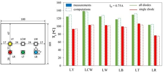
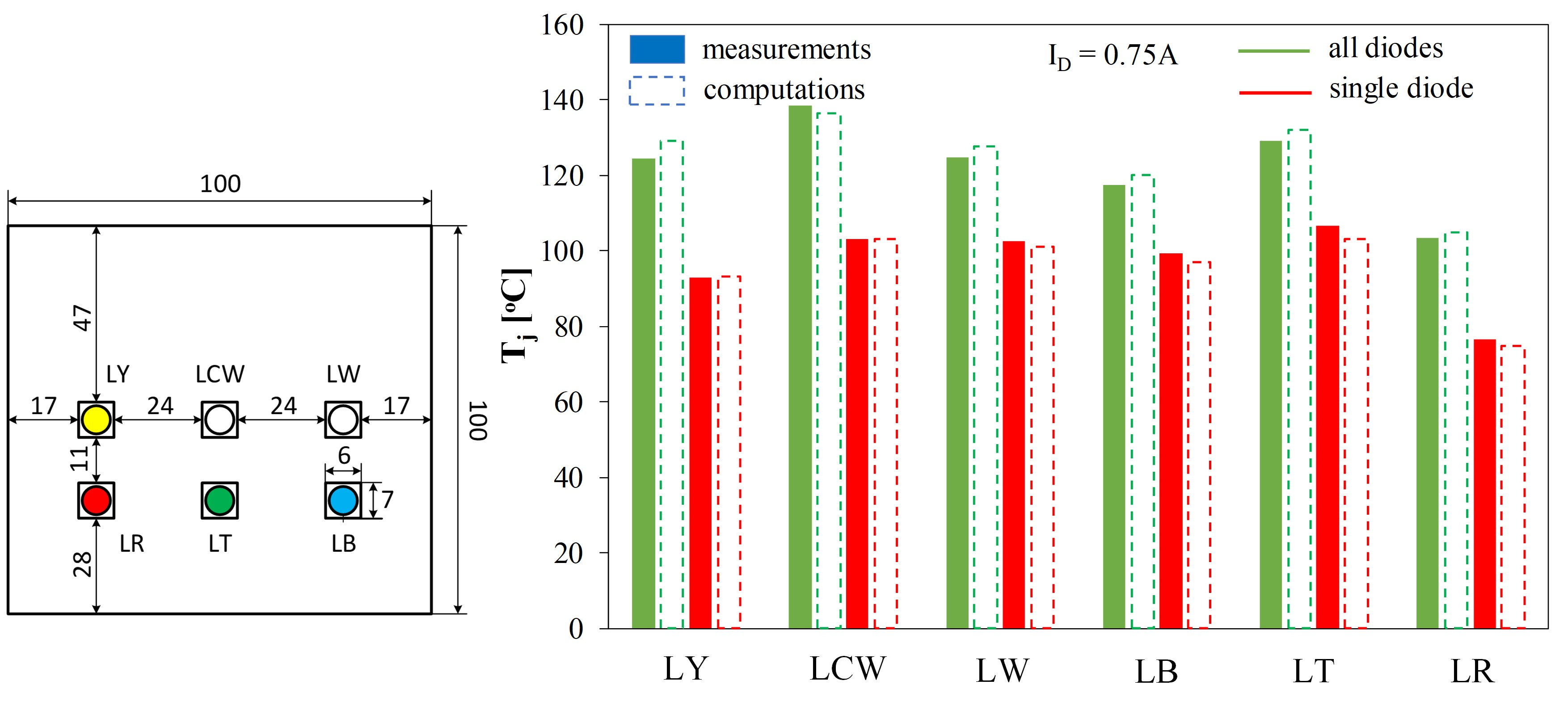
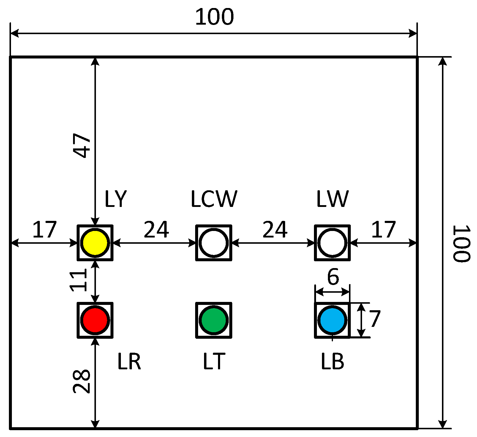
In the investigations, the mentioned diodes are mounted in the white surface packages produced from the recovered plastic material and soldered to a PCB of dimensions 100 mm × 100 mm and thickness 1.5 mm. This PCB contains an internal copper layer connecting the anodes of all the LEDs. The location of each of the considered power LEDs is shown in Figure 2.
As is visible, the investigated devices are mounted in two rows, including three LEDs situated 24 mm apart from each other. The distance between these rows is equal to 11 mm.
5. Measurement and Computation Results
To verify the usefulness of the proposed model, some computations and measurements were performed for all the mentioned power LEDs. At first, the investigations were performed for each of the investigated power LEDs operating alone. During these investigations, characteristics of the diodes were measured in the set-up shown in [48].
5.1. Measurement Set-Up
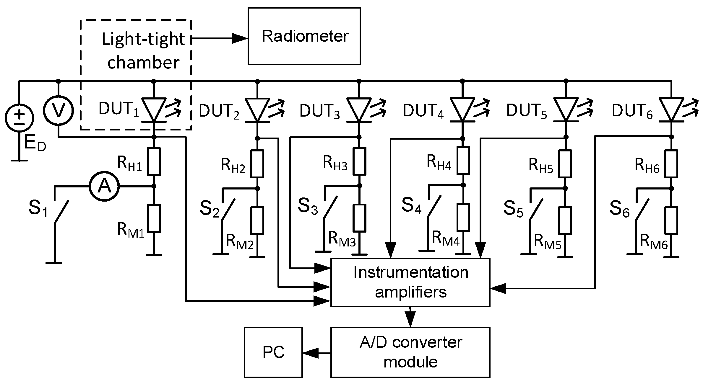
The DC–voltage characteristics of the investigated devices are measured in the thermally steady state with the use of the set-up shown in Figure 3. Simultaneously, the surface power density of the emitted light and the junction temperature of these diodes are measured. During the measurements, the investigated diodes are situated in a light-tight chamber.
The probe of a radiometer is situated in the axis of the investigated diodes. A radiometer of the type HD2302 by DeltaOhm (Caselle di Selvazzano, Italy) [56] is used. It makes it possible to measure radiation in a spectral range from 400 to 1050 nm. The calibration uncertainty is lower than 5%. The junction temperature of each diode is measured using the indirect electrical method [48,60].
The thermo-sensitive parameter used in this method is the forward voltage VF of the diode biased with current IM of a low value. This voltage nearly linearly depends on temperature [17,19,51]. Before starting the measurements, the calibration curves VF(T) of each diode must be measured. The slopes of these curves, αF, are calculated. During the calibration, all the switches are opened and the diodes are situated in a thermal chamber. The temperature of this chamber can be regulated.
If any DC characteristic of the diode DUTi is measured, switch Si is closed and the heating current IH flows through this diode until a thermally steady state is obtained. The value of the diode current IH is measured with the use of an ammeter, whereas the forward voltage VH on the diode is measured with a voltmeter.
To measure the junction temperature of these diodes, immediately after switching off switches S1–S6, the diode’s forward voltage VC is measured at the forward current IM flowing through these diodes. With the use of the measured waveform VC(t) and the thermometric characteristic VF(T), waveforms of the junction temperature Tj(t) of each diode are calculated using the formula
where Ta denotes ambient temperature.
In the set-up shown in Figure 3, ED is the power supply voltage. The investigated power LEDs are denoted as DUT1–DUT6. Resistors RH1–RH6 and RM1–RM6 are used to regulate the heating current IH and the measuring current IM of each diode, respectively. In measurement set-ups used to measure the internal temperature of semiconductor devices with indirect electrical methods, commonly presented in the literature [11,19,60], the main current of these devices in the form of a rectangular pulse train is obtained using two switched current sources. As is commonly known, it is impossible to construct a current source with a constant value of output current obtained in a wide range of voltages on such a source. Therefore, typically, such current sources are realised with the use of voltage sources and resistors, as shown in Figure 3. There are measuring devices with the ability to generate constant current over a wide voltage range, like Keithley 2400 and 2600, but these devices are expensive; the solution illustrated in Figure 3 is simpler and less costly.
In the presented set-up, current IMi is equal to the quotient of voltage equal to ED–VDi and the sum of resistances RHi and RMi. In turn, the current IHi is equal to the quotient of voltage equal to ED – VDi and the resistance RHi. Due to a high value of the voltage ED, the values of currents IHi and IMi practically do not change by more than by 2% during the measurement. Therefore, we can say that the investigated LEDs operate at feeding from current sources of a fixed value of output current.
If only one diode is heated, switch S1 is closed and other switches are opened. In contrast, if all the diodes are heated together, all the switches are closed.
In the presented measurement set-up, fast power metal-oxide semiconductor field-effect transistors (MOSFETs) are used as switches S1–S6. When such switches are turned off, the resistance connected in series with each of the investigated diodes increases by about 100 times. The used value of resistance RMi is equal to about 1 kΩ. The internal capacitance of the diode typically does not exceed 10 nF. This means that the switching-off time of this diode should not exceed 100 μs. Therefore, the measured waveforms Tj(t) should not be disturbed by the electrical transients for time t > 100 μs.
5.2. Measurement and Computation Results
In the next part of this section, selected results of the measurements (points) and computations (lines) are presented in Figure 4, Figure 5, Figure 6, Figure 7, Figure 8, Figure 9, Figure 10 and Figure 11. The computations and measurements were performed for all the investigated power LEDs operating alone (Figure 4, Figure 5, Figure 6, Figure 7, Figure 8 and Figure 9) and together (Figure 10 and Figure 11).
Figure 4 presents I–V characteristics of the tested diodes obtained in a thermally steady state.
As can be observed, a good match of the computed and measured characteristics is obtained. It is worth noticing that the forward voltage of LR and LY diodes is much lower than that of the other diodes. The highest value of the diode’s forward voltage is obtained for the LB diode. In contrast, the series resistances (determining the slope of these characteristics) of LR and LY diodes are much higher than those of the other diodes. In the characteristics presented in the lin-log scale, one can observe visible differences between measured and computed results for LT, LCW and LW diodes. These differences are a result of a simple form of the electrical model, in which the second-order phenomena are omitted. On the other hand, this simplification is justified because the considered semiconductor devices should operate in the range of high values of diode current, in which high optical power is emitted.
The observed differences between I–V characteristics obtained for the tested diodes emitting light of different colours are connected with different values of the band-gap voltage Vgo of the materials used to construct these diodes. Using I–V characteristics of the tested LEDs measured for four values of ambient temperature in the range from 25 to 100 °C, the values of the parameters characterising the electrical model are estimated using a local estimation idea. The estimated values of voltage Vgo, together with the other parameters of the electrical model of the investigated LEDs, are collected in Table 2. As seen, the values of the parameter Vgo belong to the range from 2.04 to 3.37 V. In turn, the values of the parameter n belong to the range from 2.4 to 5.3. The series resistance RS0 changes from 0.15 Ω for the LT diode to 0.46 Ω for the LR diode.
Figure 5 illustrates the influence of the estimated values of the parameter Ee0, to which the optical power of the emitted light is proportional, on the central wavelength of the emitted light for all the tested LEDs. The coefficient of determination for the measured and computed dependence is R2 = 0.86.
As can be seen, the considered dependence can be properly approximated with the use of a square function. The values of the parameter Ee0 for these diodes change in the range from 2 to 22 W/m2. The minimum of the considered dependence is observed at the wavelength corresponding to the LY diode. The observed differences in the values of the Ee0 parameter result from the properties of the used semiconductor materials and their external quantum efficiency (EQE). From the literature, it is known that the EQE is the highest for blue LEDs and the lowest for green LEDs [61]. In turn, diodes emitting white light are characterised by different values of Ee0. For the LW diode, the parameter Ee0 is nearly twice that for the LCW diode, emitting warm white light. This means that for diodes characterised by a higher value of the CCT, higher values of the Ee0 parameter are observed. It is also worth noticing that for all the considered devices, the parameter αL has the same value.
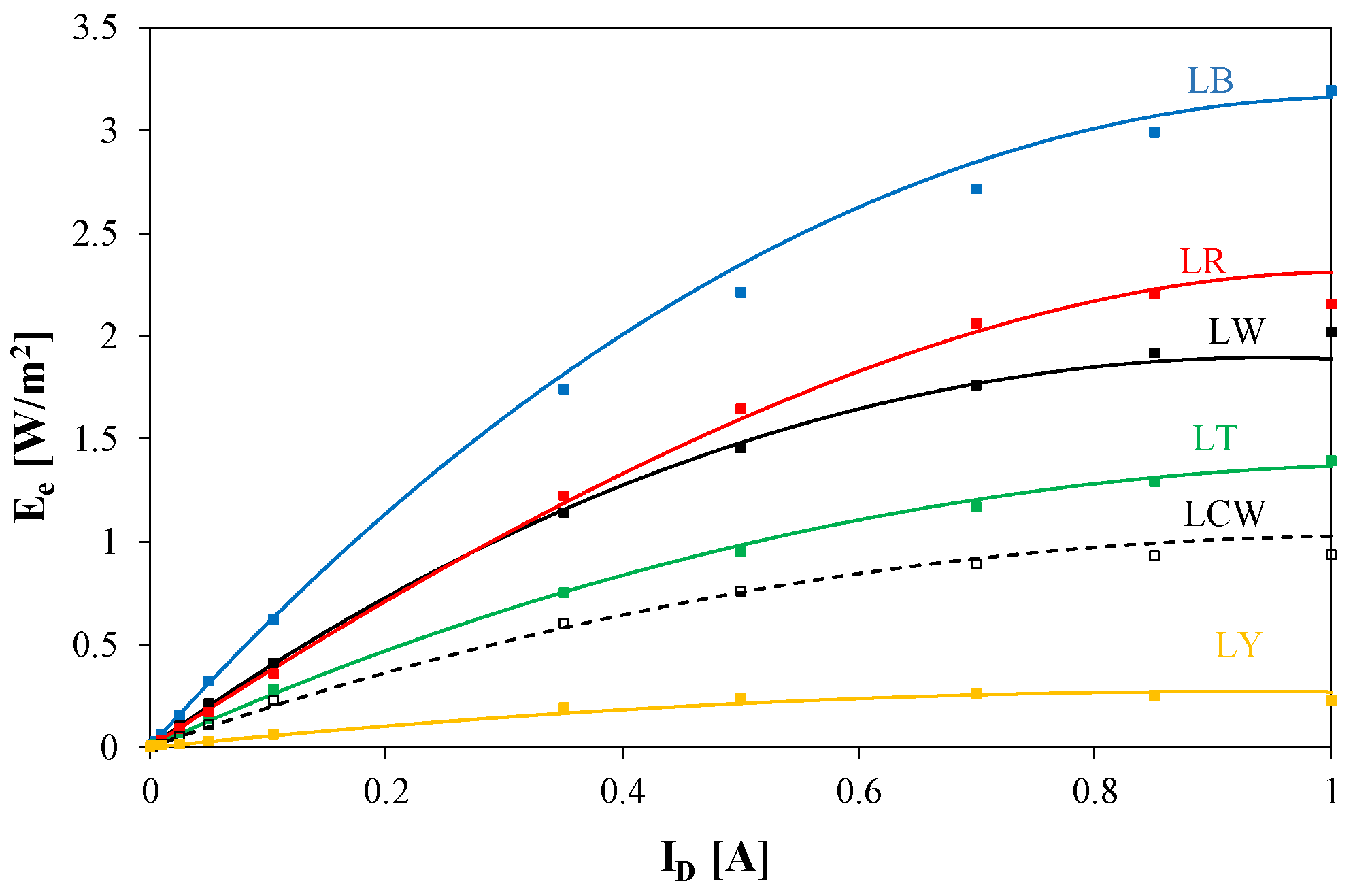
The dependence of the surface power density Ee on the area illuminated by the tested diodes in their axes on their forward current is shown in Figure 6.
As is visible, the values of Ee for the investigated diodes differ from each other, even by 1400%. The considered parameter has the highest value for the LB diode and the lowest value for the LY diode. The dependence Ee(ID) is an increasing function for each diode, but the slope of the considered characteristics is a decreasing function of the forward current. Results of computations and measurements fit well, and the average relative absolute difference between these results changes from 2.9% for the LW diode to 9.6% for the LY diode.
For the designers and users of power LEDs, it is very important to obtain a high value of watt-hour efficiency of the conversion of the electrical energy into light, ηopt. This parameter is equal to the quotient of the optical power Popt of the emitted light and the electrical power (equal to the product of forward voltage VD and forward current ID) supplying the investigated diodes. The dependence of this parameter on forward current is shown in Figure 7.
For many investigated LEDs, a good agreement between the results of measurements and the results of computations is obtained. Big differences, which do not exceed 10%, are observed only for LR and LT diodes for low values of forward current. In this range of forward current, low values of optical power are observed and the relative uncertainty of measurements of this power could be high due to the resolution of the used radiometer. It is worth observing that the results of the measurements presented in Figure 7 show that the dependence ηopt(ID) is the maximum at ID in the range between 10 and 20 mA. Unfortunately, our model does not properly describe this phenomenon. The results of the computations show that the considered dependence is a decreasing function of forward current. It is visible that LR and LB diodes are characterised by the highest values of ηopt, whereas the LY diode is characterised by the lowest value of this parameter. Results of computations and measurements fit well, and the average relative absolute difference between these results changes from 4.2% for the LW diode to 10.7% for the LY diode.
Figure 8 illustrates the dependence of the estimated values (points) of the self-electrical thermal resistance of the considered power LEDs on the central wavelength of the light emitted by these diodes. The coefficient of determination for the measured and computed dependence is R2 = 0.96.
As is visible, values of Rthe of the considered power LEDs depend on the wavelength of the emitted light. The values of the mentioned parameter for the considered diodes differ even by 20%. As is known, values of electrical thermal resistance of power LEDs depend both on the thermal properties of the used case and the other components of the heat flow path and on the relationship between the electrical power Pe consumed by the investigated device and the power of the emitted light, Popt. The power of the emitted light is high for power LEDs characterised by a high value of EQE. Therefore, at the same values of power Pe, different values of the heating power Pth = Pe − Popt are obtained. At the same efficiency of heat removal, the higher the EQE, the lower the increase in the junction temperature Tj of the investigated power LEDs at the same value of Pe. Therefore, the values of Rthe are lower for power LEDs of higher EQE.
As shown, the dependence Rthe(λmax) can be effectively approximated with a square function. The maximum of this function is observed for the diodes emitting light of wavelength equal to about 550 nm. The observed differences in the values of Rthe are a result of differences in the ηopt parameter for the considered devices and the location of these diodes on the investigated PCB.
The waveforms of the junction temperature Tj of the investigated diodes are shown in Figure 9. These waveforms are determined while cooling the investigated devices after obtaining a thermally steady state at forward current equal to 1 A.
Due to different values of electric thermal resistance and forward voltage of the investigated diodes, various values of Tj at the beginning of the cooling process are observed. The mentioned differences between the values of Tj are equal to even 25 °C. The lowest value of Tj is observed for the LR diode, whereas the highest value is observed for the LT diode. The discrepancies are also visible in the course of Tj(t) for different diodes resulting from different values of thermal capacitances characterising each investigated LED. For each considered diode, the thermally steady state is obtained after 1500 s once the cooling starts.
The results of computations and measurements presented further illustrate the influence of thermal couplings between the investigated diodes on the junction temperatures of these diodes and the surface power density of the emitted light. The investigations were performed in two operating situations. In the first situation, the current ID that causes heating of the investigated LEDs flows through one diode only, whereas in the other, a current ID of the same value flows simultaneously through all the diodes situated on the common PCB.
During these measurements, the distance between the probe of the radiometer and the surface of the investigated diode is equal to 38 mm and the light-tight tube is situated between this probe and the investigated diode.
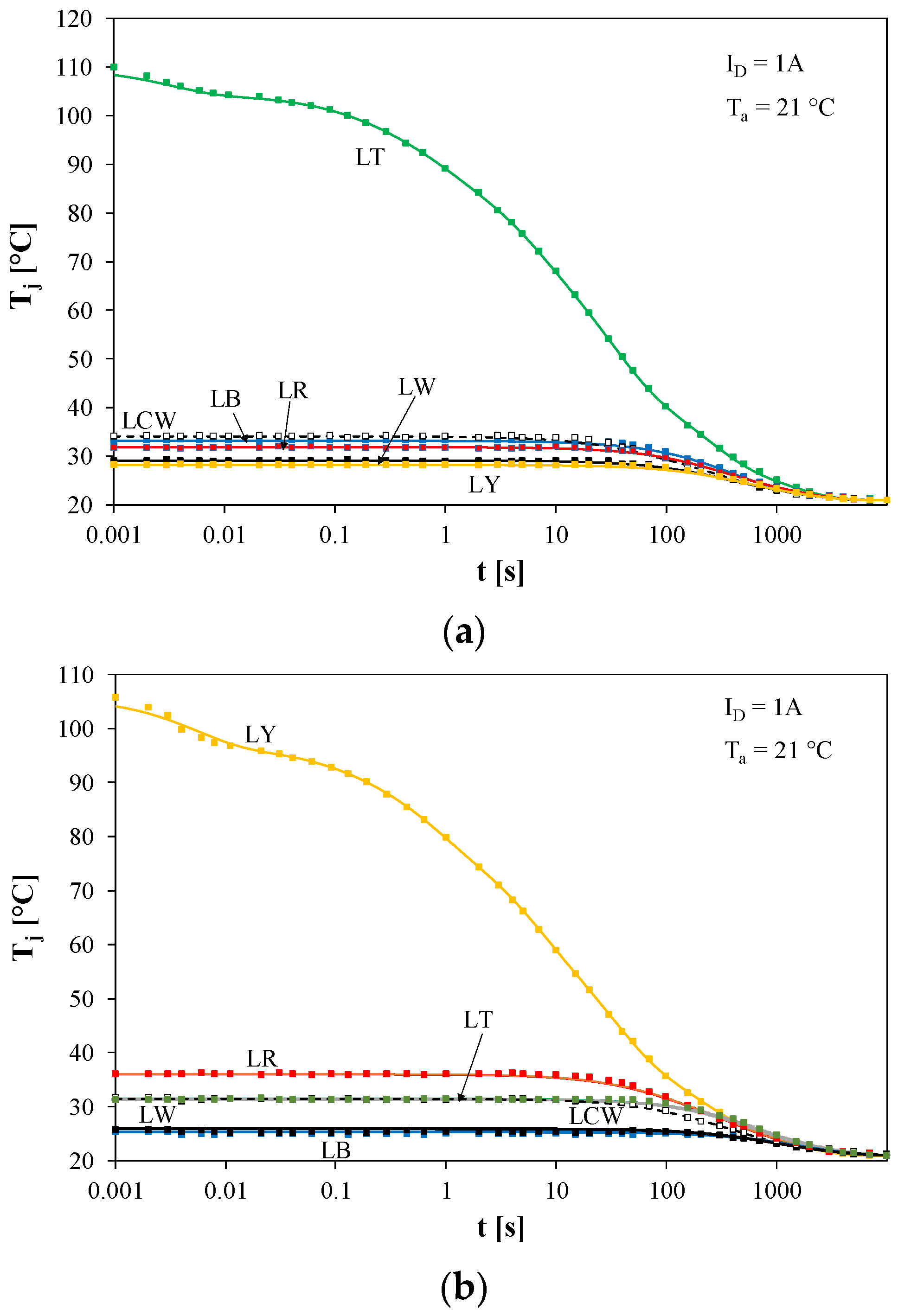
Figure 10 shows the waveform of the junction temperature of each diode situated on the tested PCB while cooling. At t = 0 in the investigated diodes, the thermally steady state is obtained after power is supplied to a single diode only—the LT diode (Figure 10a) and the LY diode (Figure 10b). In both cases current ID is equal to 1 A.
As is visible, the junction temperature of the diode to which power is supplied is much higher than ambient temperature. This is the result of self-heating phenomena. It is also visible that the junction temperatures of the other diodes are higher than ambient temperature. This is a result of mutual thermal couplings between the diodes situated on the common PCB. As shown in Figure 2, the LY diode is situated near the edge of the PCB, whereas the LT diode is situated near the centre of this PCB. Therefore, bigger differences in the values of the junction temperature of the diodes to which power is not supplied (hereafter called sensors) are observed in the case when the LY diode is supplied with power (hereafter called the heater). In this case, these differences exceed even 10 °C, whereas in the other considered case, such differences are smaller than 5 °C. It is worth observing that the junction temperatures of the sensors situated at the same distance from the heater are nearly the same. It is also shown that the influence of mutual thermal couplings on the internal temperatures of power LEDs is weaker when the distance between the heater and the sensor decreases. It is also worth observing that the junction temperature of unpowered LEDs starts decreasing by about 10 s after the power feed to the heater is switched off. This delay in changing the junction temperature of the unpowered LEDs is a result of a thermal time constant corresponding to the PCB on which the investigated diodes are mounted. The value of the considered thermal time constant depends on thermal capacitance, depending on the volume of the used PCB [62].
The results of the investigations shown in Figure 9 correspond to the operation of each and every power LED. For the investigations, the results of which are shown in Figure 9, the investigated PCB is situated inside a light-tight chamber of dimensions 400 × 250 × 220 mm3. In contrast, in Figure 10, the results of the investigations performed for the PCB lie on the table without a light-tight chamber. Due to the differences in the cooling conditions, the values of the junction temperature at the beginning of cooling (t = 0) visible in Figure 10 are lower than the values of this temperature visible in Figure 9.
To illustrate the influence of mutual thermal couplings on optical and thermal properties of the investigated semiconductor devices, some measurements and computations were performed. Values of the surface power density Εe on the surface illuminated by the emitted light and the junction temperature Tj of the investigated power LEDs were measured and computed. The investigations were performed for two cases. In the first case (marked with the red colour), a forward current ID = 750 mA flows through one power LED only. In the other case (marked with the green colour), a current of the same value flows through all the diodes simultaneously. Figure 11 presents the results of these investigations obtained in the steady state. In this figure, full bars represent the results of the measurements, whereas empty bars (with dashed lines) represent the results of the computations.
This figure also presents confidence intervals. For the measurements of Ee, the relative standard uncertainty is equal to ±6%, according to the producer’s data [56]. For temperature Tj, the standard uncertainty does not exceed ±2 °C. For both the mentioned parameters, we can estimate only type B uncertainty. We assumed a confidence level equal to 0.95, for which the coverage factor is equal to 1.96. The confidence intervals are equal to the products of standard uncertainty and coverage factor.
In Figure 11a, it is visible that an additional increase in the junction temperature of the investigated diode is a result of power dissipation in the other diodes. This increase is the smallest for the LB diode (20 °C) and the biggest for the LCW diode (40 °C). An increase in the junction temperature causes a decrease in Ee, which can be observed in Figure 11b. The biggest decrease in Ee is observed for the LR diode. This decrease is equal to even 40%. It is worth noticing that for all the considered situations, the results of the measurements and computations fit well—the differences are smaller than 10%, and typically they do not exceed the values of the confidence intervals. This confirms the correctness of the proposed model of power LEDs operating on the common PCB. It is also easy to observe that omitting the mutual thermal couplings between the power LEDs situated on a common PCB causes a big error in the computations of the junction temperature and parameters characterising the emitted light.
6. Conclusions
This paper proposes a new compact electro-thermo-optical model of multi-colour power LEDs situated on a common PCB. This model has the form of a subcircuit for SPICE, and this makes it possible to compute the voltage and current of the modelled diodes and selected optical parameters, e.g., optical power, as well as the junction temperature of these semiconductor devices, taking into account self-heating phenomena and mutual thermal coupling between these diodes. Using the proposed model, the temperature distribution on the tested PCB can be computed both in the steady state and at transients.
The form of the formulated model is simple, and the values of its parameters can be obtained in an easy way. In particular, the parameters characterising mutual thermal couplings between the considered LEDs depend on the distance between them. This observation means that for the diodes situated at the same distance from the modelled diodes, the common RC network in the thermal model can be used.
In contrast to the models presented in the literature, the new model uses electric self- and transfer transient thermal impedances, which can be more easily measured than the real transient thermal impedance. Additionally, the convergence of the computations is very easy to obtain. A simple method of estimating the model parameters values is also proposed.
The correctness of the elaborated model was verified experimentally for six diodes emitting light of different colours or white light of different CCTs. This verification was performed in the steady state and at transients for the diodes operating alone and the simultaneous operation of all the diodes situated on the common PCB. The presented results of measurements and computations show that for all the investigated diodes, a good match between the results of measurements and computations of the electrical, thermal and optical properties of the investigated LEDs can be obtained. It is clearly shown that the influence of self-heating phenomena and mutual thermal couplings between the diodes situated on the common PCB on the properties of all the considered power LEDs can be effectively described using the same electro-thermo-optical model proposed in this paper.
It is also shown that such parameters as Ee0 and Rthe characterising optical and thermal properties of the investigated devices depend on the central wavelength λmax of the emitted light. The dependence can be approximated with the use of square functions. The observed differences between the values of Ee0 for the investigated diodes exceed even 1500%, whereas for Rthe, these differences do not exceed 20%.
Mutual thermal couplings between the power LEDs situated on the common PCB cause a visible increase in the junction temperature of the tested diodes (even by nearly 40 °C) and a decrease in the optical power (even by 40%). It was shown that omitting mutual thermal couplings between the considered devices situated on the common PCB can cause unacceptably big overestimation of radiometric parameters characterising the emitted light and big underestimation of the device junction temperature. Additionally, the underestimation of the junction temperature causes the overestimation of the device lifetime, which can be overestimated by even 20 times.
It is also worth observing that the values of the electrical, thermal and optical parameters of the investigated diodes visibly differ from each other. For example, the band-gap voltage values differ by even 50%. In turn, the coefficients characterising optical power can differ from each other by even 16 times. The results presented in our paper were obtained with measurements and computations taking into account self-heating phenomena in each diode and mutual thermal coupling between each pair of the diodes situated on the common PCB.
Analysing the presented results, it is visible that for some diodes, the differences between the results of measurements and computations are bigger than can be expected when analysing only the influence of the measurement’s uncertainty. This shows that our model is not perfect, because it omits some physical phenomena occurring in the investigated devices, e.g., nonlinearity of the heat transfer generated in power LEDs to the surroundings. Yet, the obtained differences between the results of measurements and computations do not exceed the values acceptable for engineers and the time of computations is acceptably long.
In our model, we do not take into account the influence of junction temperature on the efficiency of heat removal that is dissipated in the considered devices. Yet, in our previous studies [12,26,48,63], we showed that the thermal resistance Rth decreases with an increase in the junction temperature, even by 25%. This means that due to this effect, an increase in the device’s junction temperature Tj is lower than in the case of using the linear thermal model. In further investigations, we will formulate an electro-thermal model of the considered devices, taking into account the dependence Rth(Tj).
The proposed model can be used to model the characteristics of power LEDs emitting white and colour light with good accuracy and can help engineers working on lighting systems. It can be also used in didactics to illustrate selected properties of such semiconductor devices for students. The form of the proposed model is dedicated for SPICE, but it can be adapted for different simulation tools, e.g., MATLAB and PSIM.
Author Contributions
Conceptualization, K.G.; methodology, K.G. and P.P.; measurements, P.P.; computations, K.G. and P.P.; resources, P.P.; writing—original draft preparation, K.G. and P.P.; writing—review and editing, K.G. and P.P.; visualization, K.G. and P.P.; supervision, K.G. All authors have read and agreed to the published version of the manuscript.
Funding
The project was financed within the program of the Ministry of Science and Higher Education called Regionalna Inicjatywa Doskonałości in the years 2019–2022; project number 006/RID/2018/19; sum of financing 11 870 000 PLN.
Institutional Review Board Statement
Not applicable.
Informed Consent Statement
Not applicable.
Data Availability Statement
Data are contained within the article.
Conflicts of Interest
The authors declare no conflict of interest.
Nomenclature
| Tj | junction temperature |
| Ta | ambient temperature |
| Popt | optical power |
| Ee | surface power density of the emitted light |
| Zthe(t) | electrical transient thermal impedance |
| vD | forward voltage |
| iD | diode current |
References
- Schubert, E.F. Light Emitting Diodes, 2nd ed.; Cambridge University Press: New York, NY, USA, 2008. [Google Scholar]
- Weir, B. Driving the 21st century’s lights. IEEE Spectr. 2012, 49, 42–47. [Google Scholar] [CrossRef]
- Huang, J.-J.; Kuo, H.-C.; Shen, S.-C. Nitride Semiconductor Light-Emitting Diodes (LEDs). Materials, Technologies and Applications, 2nd ed.; Elsevier: Amsterdam, The Netherlands, 2018. [Google Scholar]
- Wang, K.; Liu, S.; Luo, X.; Wu, D. Freeform Optics for LED Packages and Applications; Wiley: Hoboken, NJ, USA, 2017. [Google Scholar]
- Brugnolotto, E.; Bhogaraju, S.K.; Liu, E.; Conti, F.; Pedron, D.; Signorini, R.; Elger, G. Investigation of Thermomechanical Local Stress Induced in Assembled GaN LEDs. In Proceedings of the 2019 25th International Workshop on Thermal Investigations of ICs and Systems (THERMINIC), Lecco, Italy, 25–27 September 2019; IEEE: New York, NY, USA, 2019; pp. 1–6. [Google Scholar]
- Martin, G.; Yu, J.; Zuidema, P.; Van Der Schans, M. Luminaire Digital Design Flow with Delphi4LED LEDs Multi-Domain Compact Model. In Proceedings of the 2019 25th International Workshop on Thermal Investigations of ICs and Systems (THERMINIC), Lecco, Italy, 25–27 September 2019; IEEE: New York, NY, USA, 2019. [Google Scholar]
- Dziurdzia, B.; Sobolewski, M.; Mikołajek, J.; Wroński, S. Low-voiding solder pastes in LED assembly. Solder. Surf. Mt. Technol. 2020, 32, 201–217. [Google Scholar] [CrossRef]
- Deshayes, Y.; Baillot, R.; Joly, S.; Ousten, Y.; Béchou, L. Overview on Sustainability, Robustness, and Reliability of GaN Single-Chip LED Devices. IEEE Trans. Device Mater. Reliab. 2015, 15, 621–625. [Google Scholar] [CrossRef]
- Pavelka, T.; Ptacek, M. Degradation of LED parameters during operation Brief review of currently used models and measuring methods. In Proceedings of the 2015 16th International Scientific Conference on Electric Power Engineering (EPE), Kouty nad Desnou, Czech Republic, 20–22 May 2015; IEEE: New York, NY, USA, 2015; pp. 523–526. [Google Scholar]
- Hasan, R.; Tomal, A.I. High-performance GaN-based green LEDs. In Proceedings of the 2017 4th International Conference on Advances in Electrical Engineering (ICAEE), Dhaka, Bangladesh, 28–30 September 2017; IEEE: New York, NY, USA, 2017; pp. 54–58. [Google Scholar]
- Lasance, C.J.M.; Poppe, A. Thermal Management for LED Applications; Springer Science Business Media: New York, NY, USA, 2014. [Google Scholar]
- Górecki, K.; Ptak, P. New Method of Measurements Transient Thermal Impedance and Radial Power of Power LEDs. IEEE Trans. Instrum. Meas. 2019, 69, 212–220. [Google Scholar] [CrossRef]
- Janicki, M.; Torzewicz, T.; Samson, A.; Raszkowski, T.; Napieralski, A. Experimental identification of LED compact thermal model element values. Microelectron. Reliab. 2018, 86, 20–26. [Google Scholar] [CrossRef]
- Narendran, N.; Gu, Y. Life of LED-Based White Light Sources. J. Disp. Technol. 2005, 1, 167–171. [Google Scholar] [CrossRef]
- Zhao, M.; Zhong, S.; Fu, X.; Tang, B.; Pecht, M. Deep Residual Shrinkage Networks for Fault Diagnosis. IEEE Trans. Ind. Informatics 2019, 16, 4681–4690. [Google Scholar] [CrossRef]
- Chang, M.-H.; Das, D.; Varde, P.; Pecht, M. Light emitting diodes reliability review. Microelectron. Reliab. 2012, 52, 762–782. [Google Scholar] [CrossRef]
- Blackburn, D.L. Temperature measurements of semiconductor devices—A review. In Proceedings of the Twentieth Annual IEEE Semiconductor Thermal Measurement and Management Symposium (IEEE Cat. No.04CH37545), San Jose, CA, USA, 11 March 2004; Institute of Electrical and Electronics Engineers (IEEE): New York, NY, USA, 2004; pp. 70–80. [Google Scholar]
- Székely, V. A new evaluation method of thermal transient measurement results. Microelectron. J. 1997, 28, 277–292. [Google Scholar] [CrossRef]
- JEDEC. Standard JESD51-52: Guidelines for Combining CIE 127-2007 Total Flux Measurements with Thermal Measurements of LEDs with Exposed Cooling Surface. 2012. Available online: https://www.jedec.org/document_search?search_api_views_fulltext=Standard+JESD51-52 (accessed on 12 October 2020).
- JEDEC. Standard JESD51-51: Implementation of the Electrical Test Method for the Measurement of Real Thermal Resistance and Impedance of Light-Emitting Diodes with Exposed Cooling. 2012. Available online: https://www.jedec.org/document_search?search_api_views_fulltext=Standard+JESD51-51 (accessed on 12 October 2020).
- CREE. Thermal Management of Cree® XLamp® LEDs. Application Note CLD-AP05REV 3M. Available online: https://www.cree.com/led-components/media/documents/XLampThermalManagement.pdf (accessed on 11 February 2021).
- Efremov, A.A.; Bochkareva, N.I.; Gorbunov, R.I.; Lavrinovich, D.A.; Rebane, Y.T.; Tarkhin, D.V.; Shreter, Y.G. Effect of the joule heating on the quantum efficiency and choice of thermal conditions for high-power blue InGaN/GaN LEDs. Semiconductors 2006, 40, 605–610. [Google Scholar] [CrossRef]
- Treurniet, T.; Lammens, V. Thermal management in color variable multi-chip led modules. In Proceedings of the Twenty-Second Annual IEEE Semiconductor Thermal Measurement And Management Symposium, Dallas, TX, USA, 14–16 March 2006; IEEE: New York, NY, USA, 2006. [Google Scholar]
- Alexeev, A.; Onushkin, G.; Linnartz, J.-P.; Martin, G. Multiple Heat Source Thermal Modeling and Transient Analysis of LEDs. Energies 2019, 12, 1860. [Google Scholar] [CrossRef] [Green Version]
- Wang, C.-P.; Kang, S.-W.; Lin, K.-M.; Chen, T.-T.; Fu, H.-K.; Chou, P.-T. Analysis of Thermal Resistance Characteristics of Power LED Module. IEEE Trans. Electron Devices 2013, 61, 105–109. [Google Scholar] [CrossRef]
- Górecki, K.; Zarębski, J.; Górecki, P.; Ptak, P. Compact Thermal Models of Semiconductor Devices—A Review. Int. J. Electron. Telecommun. 2019, 65, 151–158. [Google Scholar] [CrossRef]
- Poppe, A.; Zhang, Y.; Wilson, J.; Farkas, G.; Szabo, P.; Parry, J.; Rencz, M.; Szekely, V. Thermal Measurement and Modeling of Multi-Die Packages. IEEE Trans. Components Packag. Technol. 2009, 32, 484–492. [Google Scholar] [CrossRef] [Green Version]
- Schweitzer, D.; Ender, F.; Hantos, G.; Szabó, P.G. Thermal transient characterization of semiconductor devices with multiple heat sources—Fundamentals for a new thermal standard. Microelectron. J. 2015, 46, 174–182. [Google Scholar] [CrossRef]
- Rashid, M.H. Spice for Power Electronics and Electric Power; CRC Press: Boca Raton, FL, USA, 2006. [Google Scholar]
- Górecki, K.; Ptak, P. New dynamic electro-thermo-optical model of power LEDs. Microelectron. Reliab. 2018, 91, 1–7. [Google Scholar] [CrossRef]
- Poppe, A. Multi-domain compact modeling of LEDs: An overview of models and experimental data. Microelectron. J. 2015, 46, 1138–1151. [Google Scholar] [CrossRef]
- Poppe, A. Simulation of LED based luminaries using their multi-domain compact models and CTMs of their thermal environment. Microelectron. Reliab. 2017, 72, 65–74. [Google Scholar] [CrossRef]
- Hui, S.Y.; Qin, Y.X. A General Photo-Electro-Thermal Theory for Light Emitting Diode (LED) Systems. IEEE Trans. Power Electron. 2009, 24, 1967–1976. [Google Scholar] [CrossRef]
- Hui, S.Y.R.; Lee, A.T.L.; Tan, S.-C. New Dynamic Photo-Electro-Thermal Modeling of Light-Emitting Diodes With Phosphor Coating as Light Converter Part I: Theory, Analysis, and Modeling. IEEE J. Emerg. Sel. Top. Power Electron. 2020, 8, 771–779. [Google Scholar] [CrossRef]
- Górecki, K. Modelling mutual thermal interactions between power LEDs in SPICE. Microelectron. Reliab. 2015, 55, 389–395. [Google Scholar] [CrossRef]
- Górecki, K.; Ptak, P. Modelling LED lamps in SPICE with thermal phenomena taken into account. Microelectron. Reliab. 2017, 79, 440–447. [Google Scholar] [CrossRef]
- Poppe, A.; Farkas, G.; Gaál, L.; Hantos, G.; Hegedüs, J.; Rencz, M. Multi-Domain Modelling of LEDs for Supporting Virtual Prototyping of Luminaires. Energies 2019, 12, 1909. [Google Scholar] [CrossRef] [Green Version]
- Liu, S.-M.; Chou, Y.-C. Color Calibration for a Surrounding True-Color LED Display System by PWM Controls. IEEE Trans. Ind. Electron. 2014, 61, 6244–6252. [Google Scholar] [CrossRef]
- Ozluk, B.; Muslu, A.M.; Arik, M. A Comparative Study for the Junction Temperature of Green Light Emitting Diodes (LED)s. IEEE Trans. Compon. Packag. Manuf. Technol. 2019, 9, 2024–2035. [Google Scholar] [CrossRef]
- Onushkin, G.A.; Bosschaart, K.J.; Yu, J.; Van Aalderen, H.J.; Joly, J.; Martin, G.; Poppe, A. Assessment of isothermal electro-optical-thermal measurement procedures for LEDs. In Proceedings of the 2017 23rd International Workshop on Thermal Investigations of ICs and Systems (THERMINIC), Amsterdam, The Netherlands, 27–29 September 2017; IEEE: New York, NY, USA, 2017; pp. 1–6. [Google Scholar]
- Chen, H.T.; Tan, S.-C.; Hui, S.R. Analysis and Modeling of High-Power Phosphor-Coated White Light-Emitting Diodes With a Large Surface Area. IEEE Trans. Power Electron. 2014, 30, 3334–3344. [Google Scholar] [CrossRef] [Green Version]
- Lee, A.T.L.; Chen, H.; Tan, S.-C.; Hui, S.Y. New Dynamic Photo-Electro-Thermal Modeling of Light-Emitting Diodes With Phosphor Coating as Light Converter—Part II: Model Parameter Determination and Practical Verification. IEEE J. Emerg. Sel. Top. Power Electron. 2020, 8, 780–793. [Google Scholar] [CrossRef]
- Tao, X.; Hui, S.Y.R. Dynamic Photoelectrothermal Theory for Light-Emitting Diode Systems. IEEE Trans. Ind. Electron. 2011, 59, 1751–1759. [Google Scholar] [CrossRef] [Green Version]
- Chen, H.-T.; Lin, D.-Y.; Tan, S.-C.; Hui, S.Y.R. Chromatic, Photometric and Thermal Modeling of LED Systems With Nonidentical LED Devices. IEEE Trans. Power Electron. 2014, 29, 6636–6647. [Google Scholar] [CrossRef] [Green Version]
- Baran, K.; Różowicz, A.; Wachta, H.; Różowicz, S.; Mazur, D. Thermal Analysis of the Factors Influencing Junction Temperature of LED Panel Sources. Energies 2019, 12, 3941. [Google Scholar] [CrossRef] [Green Version]
- Baran, K.; Różowicz, A.; Wachta, H.; Różowicz, S. Modeling of Selected Lighting Parameters of LED Panel. Energies 2020, 13, 3583. [Google Scholar] [CrossRef]
- Farkas, G.; Bein, M.C.; Gaal, L. Multi domain modelling of power LEDs based on measured isothermal and transient I-V-L characteristics. In Proceedings of the 2016 22nd International Workshop on Thermal Investigations of ICs and Systems (THERMINIC), Budapest, Hungary, 21–23 September 2016; IEEE: New York, NY, USA, 2016; pp. 181–186. [Google Scholar]
- Górecki, K.; Ptak, P. Thermal, Photometric and Radiometric Properties of Multi-Color LEDs Situated on the Common PCB. Electronics 2020, 9, 1672. [Google Scholar] [CrossRef]
- O’Donnell, K.P.; Chen, X. Temperature dependence of semiconductor band gaps. Appl. Phys. Lett. 1991, 58, 2924–2926. [Google Scholar] [CrossRef] [Green Version]
- Schwarz, G. Estimating the Dimension of a Model. Ann. Stat. 1978, 6, 461–464. [Google Scholar] [CrossRef]
- Avenas, Y.; Dupont, L.; Khatir, Z. Temperature Measurement of Power Semiconductor Devices by Thermo-Sensitive Electrical Parameters—A Review. IEEE Trans. Power Electron. 2012, 27, 3081–3092. [Google Scholar] [CrossRef] [Green Version]
- Székely, V.; Tarnay, K. Accurate algorithm for temperature calculation of devices in nonlinear-circuit-analysis programs. Electron. Lett. 1972, 8, 470. [Google Scholar] [CrossRef]
- Székely, V. Accurate Calculation of Device Heat Dynamics: A Special Feature of the TRANZ-TRAN Circuit-Analysis Program. Electron. Lett. 1973, 9, 132–134. [Google Scholar] [CrossRef]
- Zhu, H.; Lu, Y.; Wu, T.; Guo, Z.; Zhu, L.; Xiao, J.; Tu, Y.; Gao, Y.; Lin, Y.; Chen, Z. A Bipolar-Pulse Voltage Method for Junction Temperature Measurement of Alternating Current Light-Emitting Diodes. IEEE Trans. Electron Devices 2017, 64, 2326–2329. [Google Scholar] [CrossRef]
- Jakopovid, Z.; Bencić, Z.; Koncar, R. Identification Of Thermal Equivalent—Circuit Parameters For Semiconductors. In Proceedings of the 1990 IEEE Workshop on Computers in Power Electronics, Lewisburg, PA, USA, 5–7 August 1990; IEEE: New York, NY, USA, 2005; pp. 251–260. [Google Scholar]
- Datasheet DeltaOhm HD2302. Available online: https://www.deltaohm.com/en/wp-content/uploads/document/Del-taOHM-2302.0-Portabe-Luxmeter-Datasheet-en.pdf (accessed on 12 October 2020).
- Górecki, K.; Górecki, P. The Analysis of Accuracy of Selected Methods of Measuring The Thermal Resistance of IGBTs. Metrol. Meas. Syst. 2015, 22, 455–464. [Google Scholar] [CrossRef] [Green Version]
- Lisiecki, J.; Kłysz, S. Estimation of Measurement Uncertainty. Res. Work. Air Force Inst. Technol. 2007, 22, 62. [Google Scholar] [CrossRef] [Green Version]
- OSRAM. LT W5SM, LY W5SM, LW W5SM, LR W5SM, LB W5SM, LCW W5SM Golden Dragon, Datasheet. 2020. Available online: https://www.osram.com/ecat/Golden%20DRAGON%C2%AE%20Plus%20LCW%20W5AM/com/en/class_pim_web_catalog_103489/global/prd_pim_device_2402630/ (accessed on 11 February 2021).
- Oettinger, F.F.; Blackburn, D.L. Semiconductor Measurement Technology: Thermal Resistance Measurements; NIST/SP-400/86; U.S. Department of Commerce: Washington, DC, USA, 1990.
- Auf der Maur, M.; Pecchia, A.; Penazzi, G.; Rodrigues, W.; Di Carlo, A. Efficiency Drop in Green InGaN/GaN Light Emitting Diodes: The Role of Random Alloy Fluctuations. Phys. Rev. Lett. 2016, 116, 27401. [Google Scholar] [CrossRef] [PubMed] [Green Version]
- Liebhard, J.H., IV; Liebhard, J.H., V. A Heat Transfer Textbook, 3rd ed.; Phlogiston Press: Cambridge, MA, USA, 2008. [Google Scholar]
- Górecki, K.; Górecki, P. Nonlinear Compact Thermal Model of the IGBT Dedicated to SPICE. IEEE Trans. Power Electron. 2020, 35, 13420–13428. [Google Scholar] [CrossRef]
Figure 1.
Network representation of the electro-thermo-optical model of the power light-emitting diode (LED) situated on a common PCB (Printed Circuit Board) with m other diodes.
Figure 1.
Network representation of the electro-thermo-optical model of the power light-emitting diode (LED) situated on a common PCB (Printed Circuit Board) with m other diodes.

Figure 2.
Dimensions of the investigated PCB and the locations of the investigated power LEDs.

Figure 3.
Diagram of the used measurement set-up.

Figure 4.
Computed and measured I–V characteristics of the tested power LEDs in lin-lin (a) and lin-log (b) scales.
Figure 4.
Computed and measured I–V characteristics of the tested power LEDs in lin-lin (a) and lin-log (b) scales.

Figure 5.
Dependence of the estimated values of the parameter Ee0 of the investigated power LEDs on the central wavelength λmax of the emitted light.
Figure 5.
Dependence of the estimated values of the parameter Ee0 of the investigated power LEDs on the central wavelength λmax of the emitted light.
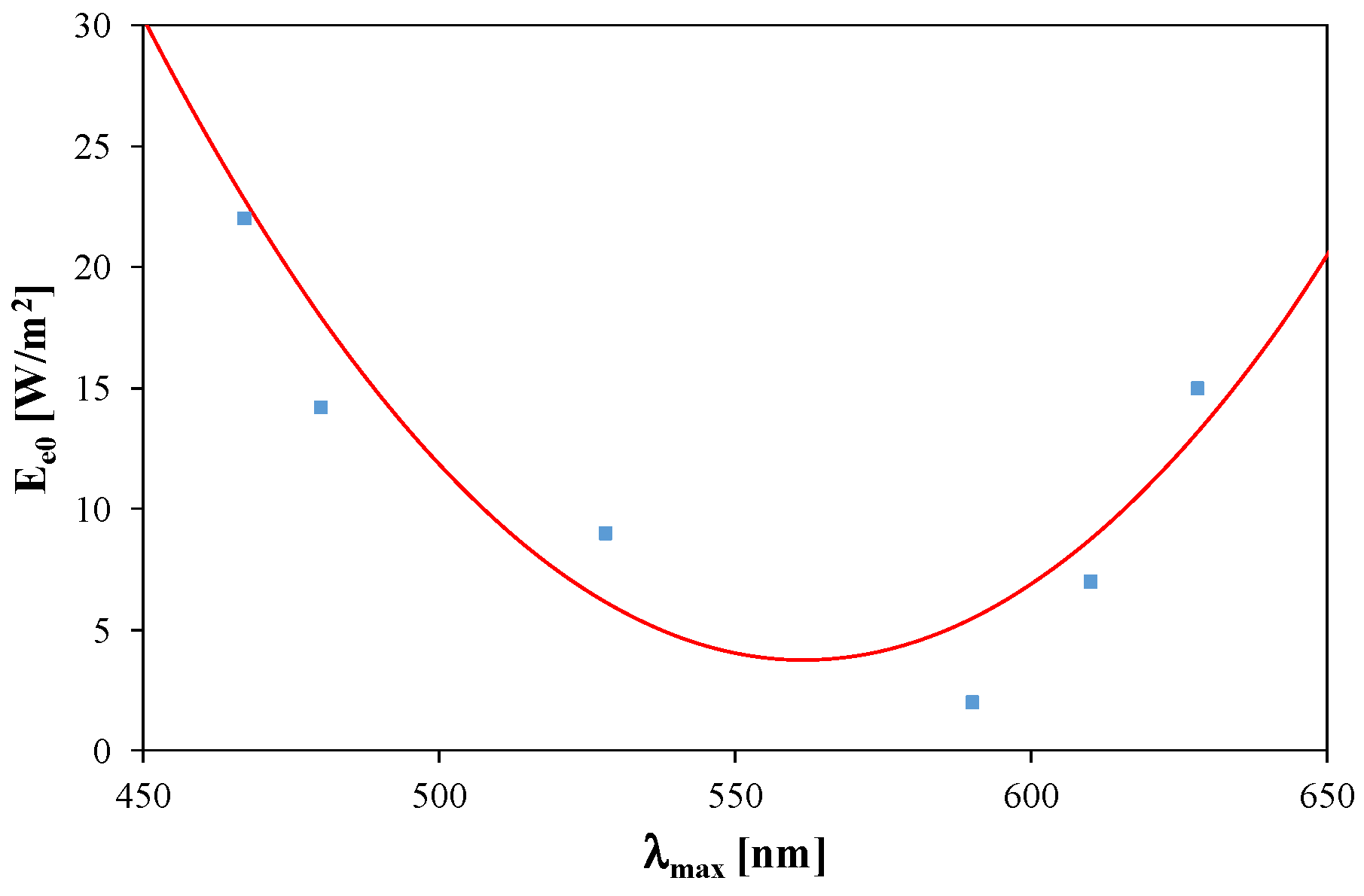
Figure 6.
Computed and measured dependence of the surface power density Ee on forward current.

Figure 7.
Computed and measured dependence of watt-hour efficiency of the conversion of electrical energy into light in the investigated power LEDs on forward current.
Figure 7.
Computed and measured dependence of watt-hour efficiency of the conversion of electrical energy into light in the investigated power LEDs on forward current.

Figure 8.
Dependence of the estimated values of the self-electrical thermal resistance Rthe of the investigated power LEDs on the central wavelength λmax of the emitted light.
Figure 8.
Dependence of the estimated values of the self-electrical thermal resistance Rthe of the investigated power LEDs on the central wavelength λmax of the emitted light.

Figure 9.
Computed and measured waveforms of junction temperatures of the considered power LEDs while cooling.
Figure 9.
Computed and measured waveforms of junction temperatures of the considered power LEDs while cooling.

Figure 10.
Computed and measured waveforms of junction temperatures of the investigated power LEDs while cooling after power is supplied to a single diode only: (a) the LT diode and (b) the LY diode.
Figure 10.
Computed and measured waveforms of junction temperatures of the investigated power LEDs while cooling after power is supplied to a single diode only: (a) the LT diode and (b) the LY diode.

Figure 11.
Computed (empty bars) and measured (full bars) values of junction temperature (a) and the surface power density of the emitted light (b) for the power LEDs operating alone and together with the other diodes situated on the common PCB.
Figure 11.
Computed (empty bars) and measured (full bars) values of junction temperature (a) and the surface power density of the emitted light (b) for the power LEDs operating alone and together with the other diodes situated on the common PCB.


Table 1.
Values of luminous flux ΦV, thermal resistance Rthj-s and central wavelength of the investigated power LEDs [59].
Table 1.
Values of luminous flux ΦV, thermal resistance Rthj-s and central wavelength of the investigated power LEDs [59].
| Diode | LR | LY | LT | LB | LW | LCW |
|---|---|---|---|---|---|---|
| Rthj-s (K/W) | 6.5 | 6.5 | 6.5 | 5 | 5 | 5 |
| ɸv (lm) | 39–71 @400 mA | 39–82 @400 mA | 52–97 @350 mA | 15–33 @350 mA | 71–130 @350 mA | 45–97 @350 mA |
| λmax (nm) | 628 | 590 | 528 | 467 | 480 | 610 |
Table 2.
Estimated values of the parameters of the electrical models for the investigated LEDs.
| Diode | LR | LY | LT | LB | LW | LCW |
|---|---|---|---|---|---|---|
| Vgo (V) | 2.04 | 2.16 | 2.63 | 3.37 | 2.79 | 2.86 |
| I0 (A) | 1.1 | 1.93 | 0.06 | 220 | 0.26 | 0.5 |
| n | 3 | 3.3 | 5.3 | 2.4 | 3.4 | 3.4 |
| RS0 (Ω) | 0.46 | 0.42 | 0.15 | 0.25 | 0.19 | 0.19 |
Publisher’s Note: MDPI stays neutral with regard to jurisdictional claims in published maps and institutional affiliations. |
© 2021 by the authors. Licensee MDPI, Basel, Switzerland. This article is an open access article distributed under the terms and conditions of the Creative Commons Attribution (CC BY) license (http://creativecommons.org/licenses/by/4.0/).
Share and Cite
MDPI and ACS Style
Górecki, K.; Ptak, P. Compact Modelling of Electrical, Optical and Thermal Properties of Multi-Colour Power LEDs Operating on a Common PCB. Energies 2021, 14, 1286. https://doi.org/10.3390/en14051286
AMA Style
Górecki K, Ptak P. Compact Modelling of Electrical, Optical and Thermal Properties of Multi-Colour Power LEDs Operating on a Common PCB. Energies. 2021; 14(5):1286. https://doi.org/10.3390/en14051286
Chicago/Turabian StyleGórecki, Krzysztof, and Przemysław Ptak. 2021. "Compact Modelling of Electrical, Optical and Thermal Properties of Multi-Colour Power LEDs Operating on a Common PCB" Energies 14, no. 5: 1286. https://doi.org/10.3390/en14051286
Note that from the first issue of 2016, this journal uses article numbers instead of page numbers. See further details here.