
Overview of Signal Processing Problems in Power Electronic Control Circuits †

Institute of Automation, Electronics and Electrical Engineering, University of Zielona Góra, ul. Szafrana 9, 65-516 Zielona Góra, Poland
†
This paper is an extended version of my paper published in the Proceedings of the 2016 Signal Processing, Algorithms, Architectures, Arrangements and Applications—SPA 2016: Conference Proceedings, University of Technology, Poznań, Poland, 21–23 September 2016, pp. 162–171.
Energies 2023, 16(12), 4774; https://doi.org/10.3390/en16124774
Submission received: 8 May 2023
/
Revised: 4 June 2023
/
Accepted: 15 June 2023
/
Published: 17 June 2023
(This article belongs to the Section F: Electrical Engineering)
Abstract
:This paper examines various aspects related to digital signal processing in digital control circuits used in power electronics. The discussion focuses on several common issues, including the sampling rate of signals (including phenomena such as aliasing and synchronization), coherent sampling, jitter of sampling pulses, sequential versus simultaneous sampling in multichannel systems, signal resolution (including signal-to-noise ratio, noise-shaping circuits, and changes in sampling speed), interpolation and decimation, and the conversion of analog circuits into digital form. One of the key contributions of this paper is the introduction of a new formula for calculating the resultant signal-to-noise ratio for three-stage digital control circuits. By carefully considering and correcting for sources of error, it is possible to increase the signal-to-noise ratio and minimize distortion components. This, in turn, leads to improved output/input current and voltage parameters, which can have a positive impact on the overall quality of energy processing in power electronic circuits.
1. Introduction
In the past, the conversion of electricity from one form to another was mainly reserved for industrial installations. Currently, with the increasing dependence of modern civilization on electricity, electricity conversion is very widespread and concerns us all. Power electronics devices that convert electricity from one form to another are everywhere these days. Starting with mobile phone chargers, power supplies for computers, electric drive systems, electric cars, electric car charging stations, and photovoltaics, we could go on for so long. Therefore, it can be said that power electronics are now very important for the current civilization. Consequently, the number of publications devoted to power electronics is enormous (e.g., [1,2,3,4,5,6,7,8,9,10]), and similarly, many publications describe problems of digital signal processing (e.g., [11,12,13,14,15,16,17,18,19,20,21,22,23,24,25,26,27]). Only a few publications describe digital signal processing in the context of power electronics [28,29,30,31,32,33,34,35,36,37,38,39,40,41,42,43,44,45,46,47].
In the paper, there is a review of the impact of selected aspects of signal processing on energy conversion by power electronic circuits. This paper is a revised and extended version of the author’s conference paper [26].
Power electronics and digital signal processing are two closely related fields, yet only a few publications describe digital signal processing in the context of power electronics. In this paper, selected aspects associated with the design and applications of digital signal processing in power electronic control circuits are discussed. Control of power electronic circuits requires great care and attention from the circuit designer, as errors in the control system can lead to a complete failure of the system.
Unfortunately, many poorly designed digital control circuits have been reported in the literature, where interference and a high noise level occur, despite not being predicted in simulations. To avoid such problems, the following aspects of digital control circuit design are presented: signal sampling rate, synchronization, signal resolution, changing of sampling speed, and conversion of analog circuits to digital form.
Understanding these aspects can greatly influence the parameters of input/output voltages and currents, leading to highly reliable power electronic circuits.
An example of such a system includes a 12-bit analog-to-digital (A/D) converter, a floating-point digital signal processor (DSP), an 8-bit pulse width modulation (PWM) output, and a sampling speed that is only slightly faster than twice the maximum signal frequency.
Despite the prevalence of fully digital control circuits, many papers still present analog control algorithms that are then implemented digitally, often overlooking key aspects associated with the transformation and implementation of digital circuits. To prevent such issues, the author has identified and presented several crucial aspects of digital control circuit design:
- (a)
- Signal sampling rate: This includes considerations such as aliasing, sequential vs. simultaneous sampling in multichannel systems, and the jitter of sampling pulses.
- (b)
- Synchronization: This involves coherent sampling.
- (c)
- Signal resolution: This includes the signal-to-noise ratio and the noise-shaping circuit.
- (d)
- Changing sampling speed: This includes interpolation and decimation.
- (e)
- Conversion of analog circuits to digital form.
All of these aspects can significantly affect the parameters of input/output voltages and currents in digital control circuits.
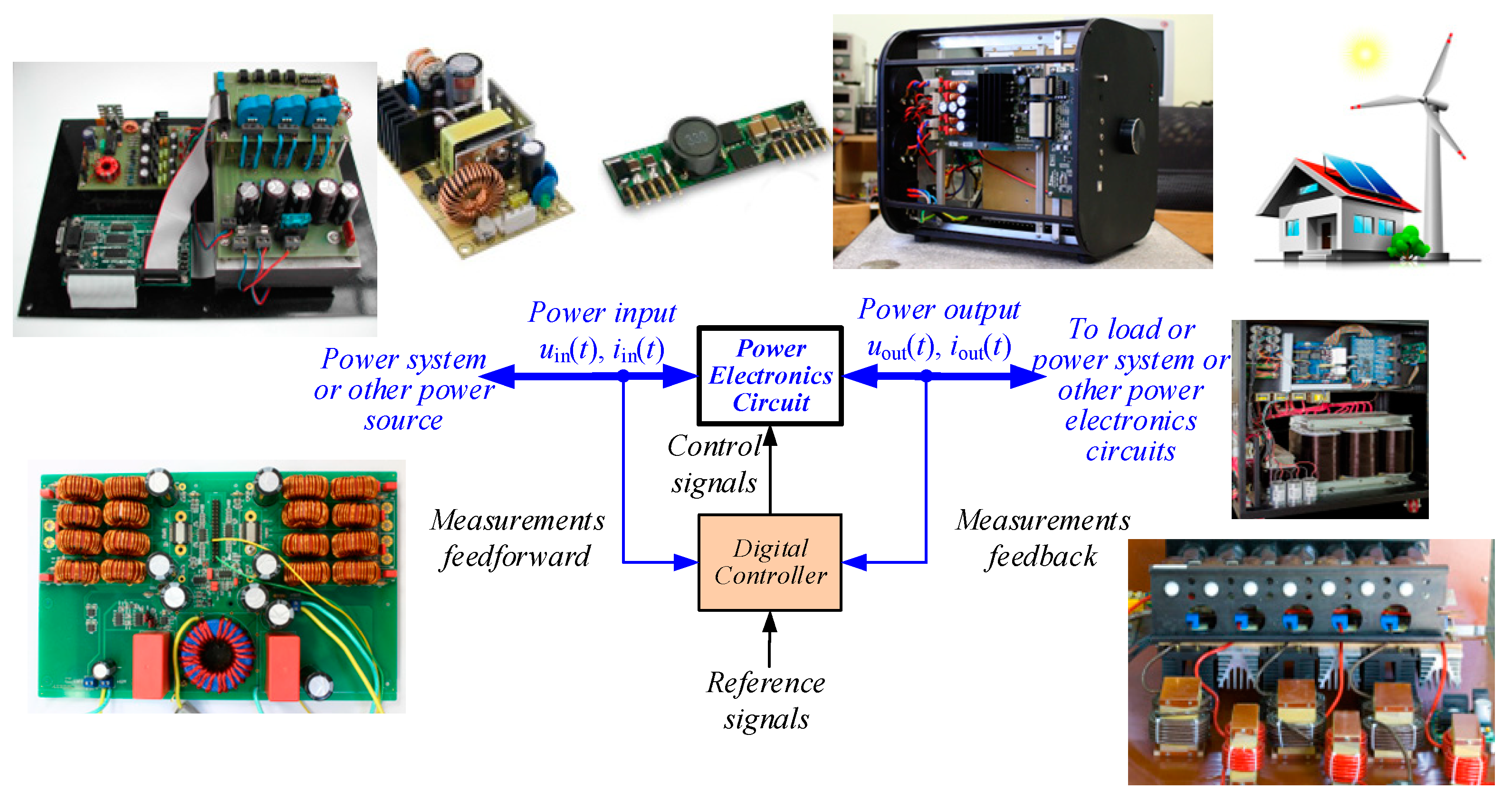
2. Power Electronic Circuit
Power electronic systems are widely used for the control and conversion of electric power. A typical block diagram of such a system is shown in Figure 1. It consists of a power electronic circuit, which includes electronic switches such as IGBTs, MOSFETs, capacitors, magnetic components, and a digital controller. The control algorithm is implemented in the digital controller, which is responsible for controlling the operation of the power electronic circuit [28,29,30,31,32,33,34,35,36,37,38,39,40,41,42,43,44,45,46,47].
The digital controller uses digital signal processing techniques to process the input signals, generate control signals, and control the output of the power electronic circuit according to the desired performance criteria. This allows for precise control of the power electronic circuit and efficient conversion of electric power for various applications such as motor drives, renewable energy systems, and power supplies.
The use of digital controllers in power electronic systems has greatly improved the performance, reliability, and flexibility of these systems, enabling advanced control strategies and enhanced functionalities.
Figure 2 shows an instance of a power electronic circuit that utilizes an open-loop multirate digital control circuit. This type of circuit is commonly used in control systems for DC/DC, DC/AC, AC/DC, and AC/AC converters, as well as active power filters, among other applications [37,42]. An open-loop system was chosen due to its ease of analysis.
It is important to note that the closed-loop circuit should also be considered, where feedback from the output is used to adjust the system’s parameters. This feedback loop can greatly improve the system’s stability and accuracy. However, closed-loop systems are often more complicated to design and analyze than their open-loop counterparts.
In this circuit (depicted in Figure 2), the analog input signal x(t) is first converted to a digital signal x(n) by an analog-to-digital (A/D) converter, which operates at a sampling ratio of fs1 and has a bit resolution of b1. The digital signal is then processed by a digital control algorithm implemented on a digital signal processor (DSP), which has a bit resolution of b2 and operates at a sampling ratio of fs2. Finally, the output control signal y(n) is transferred to a digital pulse width modulator (PWM) with a bit resolution of b3 and a sampling ratio of fs3. The PWM controls the output power switches S1 and S2, which operate at a switching frequency of fc. The digital PWM, along with an analog output filter LC, CC, functions as a power digital-to-analog (D/A) converter that converts energy from a DC source to the output.
Nowadays, there are numerous options for A/D converters and DSPs that allow for the selection of circuits with adequate parameters, including b1, b2, fs1, and fs2. However, the last stage, which involves the digital PWM (Figure 3), can still be a bottleneck for the entire system, particularly for high resolutions such as those required for a high-quality power audio amplifier (e.g., fs3 = 44.1 kHz and b3 = 16 bit). The clock frequency of PWM counters can be calculated as follows:
The required clock frequency is too high for typical digital circuits, necessitating a reduction in the resolution of the digital PWM, which results in a decline in the signal-to-noise ratio. This paper proposes a solution to this problem.
Microcontroller manufacturers noticed this problem and began to equip microcontrollers with high-resolution PWM (HRPWM). For example, the TMS320F28379D microcontroller uses an HRPWM chip with a resolution of 150 ps to 350 ps [48]. Which theoretically corresponds to a clock frequency of 2.9 GHz to 6.7 GHz. However, this is not such a precise resolution, because it is obtained partly in an analog way.
3. Selected Signal Parameters
From the point of view of the operation of the entire power electronic circuit, it is important to obtain the required parameters of input and output voltages and currents. The quality of the output voltage and current of the power electronic circuit is a critical concern, and the following signal parameters should be taken into account: the signal sampling ratios (fs1, fs2, and fs3), signal resolutions (b1, b2, and b3), transistor switching frequency (fc), total harmonic distortion ratio (THD), output signal-to-noise ratio (SNR), and output signal-to-noise and distortion ratio (SINAD) [37,49,50,51,52,53]. The required SINAD value of the output current or voltage of a power electronic circuit depends on the application. For instance, a SINAD value of 30 dB may be sufficient for a battery charger, while a high-quality class-D audio amplifier may require a SINAD value of over 100 dB. As such, the parameters of digital control systems for power electronic circuits can vary greatly.
Figure 4 shows the amplitude spectrum of an example sinusoidal signal with a fundamental frequency of f1. As you can see in the figure, the signal contains harmonics and noise. In order to determine the parameters of such a signal, the following parameters are considered: SNR, SINAD, signal dynamic range (DR), signal headroom, and THD should also be added.
3.1. SINAD
The previous paragraphs have discussed only linear circuits, but in practice, it is always possible to encounter nonlinearity; hence, it is crucial to take into account the influence of harmonics on signal dynamics. The parameter which completely describes the space between the signal and interference is the signal-to-noise and distortion ratio (SINAD) [37,49,50,51,52,53]. SINAD is the ratio of the wanted signal (the fundamental) to the sum of all distortion and noise products after the DC term is removed. SINAD is a measure of the quality of a signal, defined as follows:
where Px, Pn, and Pd—averages of the resultant power values of the signal, noise, and distortion components, respectively.
3.2. SNR
The signal-to-noise ratio (SNR) is defined as the ratio of the power of a signal (meaningful input) to the power of background noise:
where Px and Pn—averages of the resultant power values of the signal and noise.
3.3. DR
The dynamic range of a signal processing system can be defined as the ratio of the maximum signal level sustainable without overflow (or other distortion) to the minimum signal level:
where |Xmax|—maximum amplitude of the signal (in digital systems, typically the most significant bit, MSB, is used) and |Xmin|—minimum amplitude of the signal (the least significant bit, LSB, in digital systems).
3.4. THD
This is another parameter characterizing the quality of the signal: total harmonic distortion (THD). It determines the ratio of the effective harmonic value to the effective value of the signal:
where U1—amplitude of the fundamental component and U2, U3, and U4 …—amplitudes of the harmonics.
4. Signal Sampling
In a control system that uses uniform sampling, a continuous analog signal is sampled at discrete intervals of Ts = 1/fs. It is crucial to carefully choose the sampling frequency fs to ensure an accurate representation of the original analog signal. The sampling frequency should be at least twice the highest frequency fb of the analog signal [54,55,56,57,58]. Increasing the number of samples taken (i.e., higher sampling rates) results in a more accurate digital representation, while reducing the number of samples (i.e., lower sampling rates) can lead to critical information loss.
In classical systems, for an analog signal band of 0…fb, the Nyquist frequency (fs/2) is only slightly higher than fb. In sampled data systems, the input signal’s spectrum is folded around a frequency that is one-half that of the sampling clock. Figure 5 shows the spectrum of a sampling process with aliasing phenomena. An ideal input low-pass anti-aliasing filter (Figure 2) should pass all signals in the band of interest and block all signals outside of that band. The quality of the input anti-aliasing low-pass filter is a significant factor that contributes to the quality of a digital signal. The attenuation in the stop-band (for frequency f > fb) of the input anti-aliasing filter depends on the required SNR:
where Px—power of the signal and Pa—power of aliasing components.
4.1. Oversampling
In the past, digital systems operated by sampling analog signals at frequencies close to the maximum signal frequency. This meant that the analog input and output filters needed to meet very high requirements. However, with the advancement of technology, digital systems are becoming faster and faster, making it easy and cost-effective to increase the sampling rate [12,13,14,21,22,37]. This, in turn, reduces the requirements for the analog input and output filters. Oversampling is a technique used to achieve this. In oversampling, the signal with a frequency band of 0 … fb is sampled at a frequency much higher than 2fb. The oversampling ratio (R) is calculated using the following equation:
In oversampling, the sampling frequency (fs) is chosen to be much higher than twice the bandwidth of the signal (2fb), resulting in a higher oversampling ratio (R). This allows for more samples to be taken within the bandwidth of interest, resulting in a higher-resolution representation of the signal.
The utilization of oversampling in a system, as demonstrated in Figure 6, can result in analog filter characteristics that are softer, thereby lowering the complexity and cost associated with such filters. This reduction in filter requirements, in turn, can lead to an improvement in the performance of the control system and a decrease in overall system cost. The use of oversampling also has the potential to increase the resolution of the digital system, which can enable more accurate signal control and measurement.
By increasing the oversampling ratio, the requirements for the analog input and output filters can be reduced. This is because the higher sampling rate captures more information about the signal, including higher-frequency components that may have been filtered out in lower oversampling ratios. This can result in improved signal-to-noise ratio and dynamic range in the digital system, without the need for complex and expensive analog filters.
Oversampling is a technique commonly used in modern digital systems, such as audio and video processing, data communication, and sensor applications, to achieve higher accuracy and performance while reducing the requirements on analog components.
4.2. Simultaneous Sampling
In systems, it is often necessary to covert several analog signals. For example, if current and voltage are being converted, it should be performed at the same sampling time. Therefore, in multichannel systems, it is very important that the input signals are simultaneously sampled to reduce amplitude and phase errors. In analog input design, the A/D converters have two very common architectures: one using multiplexed (sequential) and the other using simultaneous sampling solutions [37,49,50]. Figure 7 shows two examples of systems for measuring current and voltage, one with simultaneous sampling (Figure 7a) and the other with sequential sampling (Figure 7b).
Multiplexed architectures use one A/D converter for many channels. A sampling illustration of two analog signals is depicted in Figure 8. The main disadvantage of a sequential-sampling A/D converter is the time delay between different channel samples.
The maximum error value of the amplitude of a sinusoidal signal can be calculated by the following formula [37]:
where f—sinusoidal signal frequency, tc—the time delay between sample impulses, and AF—amplitude of the sinusoidal signal.
The best solution is to use a simultaneous sampling A/D converter, in which samples are taken at the same moment in time. The benefits of simultaneous sampling compared to sequential sampling include less jitter, higher bandwidth, less channel-to-channel crosstalk, and less settling time. However, if simultaneous sampling is not possible to implement, the sequential sampling A/D converter with time alignment has to be implemented instead.
For a b-bit system with sequential sampling, assume that the signal error should be less than half LSB [37].
For a b-bit system with sequential sampling, assume that the signal error should be less than half LSB [6].
The problem of the advantages of simultaneous sampling has also been noticed by leading manufacturers of microcontrollers. For example, the TMS320F283xx family of microcontrollers from Texas Instruments has been equipped with four A/D converters that allow simultaneous sampling of four analog signals [48]. Of course, it would be good if microcontrollers with six A/D converters were developed, allowing simultaneous measurement of three currents and three voltages in three-phase systems. However, even four converters allow the implementation of the three-phase active power filter (APF) control system [59].
4.3. Synchronization of the Sampling Process
The coherence of sampling (when fs = kf, where k—integer) has a significant impact on the behavior of digital signal processing algorithms such as the discrete Fourier transform (DFT) [37,60,61,62]. An exemplary spectrum of a coherently sampling sinusoidal signal is depicted in Figure 9a. When sampling is not coherent, it can cause spectral leakage, resulting in unwanted phenomena as depicted in Figure 9b. Therefore, the author suggests that synchronization should be employed in systems connected to the power network.
Figure 9c shows a block diagram of a digital control circuit that employs synchronization, utilizing a phase-locked loop (PLL) to generate an output signal whose phase is linked to the phase of an input signal. The PLL produces signals with frequencies that are integer multiples of the power line voltage frequency. Additionally, the DSP clock is synchronized with the power line voltage in this circuit. By utilizing synchronization effectively, the system’s properties can be enhanced while avoiding unwanted components, such as beat frequencies.
It should be noted that such a system has indisputable advantages, but the behavior of such a system in transient states should also be considered. Typically, before the system is fully synchronized, slowly changing oscillations may occur. For example, for systems synchronized to the voltage frequency in the mains, you can consider abandoning such a system because, currently, the frequency of the mains voltage is very stable (about ±50 mHz) [59].
4.4. Hard Real-Time System
As previously stated, the control circuit of a power electronic system is most important and should be designed as a hard, real-time system. This means that the control system’s hardware, software, or a combination of both must have a hard deadline for completing a task or action [19,20,37]. Failure to meet this deadline would result in task failure and, in power electronic circuits, a high risk of damage to hardware components. Figure 2 shows a block diagram of an exemplary control circuit with one analog input and one analog output, while Figure 10 depicts a typical timing diagram for such a control circuit in power electronics. During the sampling period Ts, all operations such as calculation, conversion, and communication must be completed. If the control circuit is multirate, as in Figure 2, operations must be finished during the output circuit’s Ts3 period.
4.5. Jitter
Maintaining the stability and repeatability of sampling moments is crucial for ensuring high signal quality. Any variation in the sampling moments, also known as aperture uncertainty or jitter, can result in an error voltage proportional to the magnitude of the jitter and the input signal slew rate. In real A/D converters, sampling moments are often uncertain due to hardware errors and noise, and the issues of signal uncertainty due to sampling have been discussed by numerous authors [37,63,64,65,66,67].
The most common sources of sampling signal jitter are the following:
- Software triggering of the sampling pulse;
- Unwanted electromagnetic couplings created between the traces of a printed circuit board and another source of electromagnetic noise;
- Power supply noise in electronic devices and circuits;
- Digital circuit oscillator frequency drifts over time due to noise;
- Flicker noise;
- Thermal noise.
Only the largest sources of jitter are listed. Within these jitter sources, the software triggering of sampling pulses can generate the highest jitter value.
For a high-quality digital power amplifier, the required SINAD value may be more than 100 dB. In this case, the effect of the jitter can be critical to the circuit parameters.
Figure 11 illustrates a sampling pulse clock with a jitter, while Figure 10b shows how a sampling time jitter generates a signal error. The maximum voltage error for a sinusoidal signal with frequency f and amplitude A can be calculated.
Sampling pulse jitter adds noise to the signal, and the signal-to-noise ratio for a sinusoidal signal can be calculated by the formula:
where Δtrms—root means square of time jitter.
Example 1
The case demonstrates how signal quality can deteriorate due to jitter. If we assume a signal frequency of 3 kHz, a sampling frequency of 40 kHz, and a jitter root mean square of 0.20 μs, the signal-to-noise ratio calculated from Formula (12) with a Gaussian distribution of jitter is SNR = 48.47 dB. A simulation was conducted in Matlab to illustrate this problem, and the results are shown in Figure 12. The sinusoidal signal in the spectrum of Figure 12a was coherently sampled without jitter, and its SNR of 234.40 dB is limited only by the arithmetic accuracy of Matlab. Figure 12b displays the spectrum of the signal that was sampled with jitter. In this scenario, the simulated signal-to-noise ratio is SNR = 48.47 dB with a Gaussian distribution of jitter, which is nearly identical to the value calculated from Formula (12).
It is crucial to generate sampling pulses with great precision, which can only be accomplished using appropriately designed hardware. Attempting to directly generate pulses with software or hardware-software systems may result in high levels of jitter, leading to a notable degradation of the signal-to-noise ratio.
When using microcontrollers, an internal counter is often used to generate an interrupt. The A/D converter is triggered at the beginning of the interrupt handler. This type of solution is a source of jitter. To illustrate this phenomenon, measurements were made for two TMS320F28379D from Texas Instruments and STM32G491RE from STMicroelectronics microcontrollers. The results are shown in Figure 13 and Figure 14. For STM32G491RE, Δt is about 70 ns, and for TMS320F28379D, Δt is about 15 ns. To avoid this problem, microcontrollers should be programmed so that A/D converters are triggered only by hardware, as shown in Figure 15. The entire control algorithm is implemented in the interrupt procedure generated by the A/D converter, as shown in Figure 10. After the calculations are completed, the value of the output signal y(n) controlling the PWM modulator is modified.
5. Multirate Circuits
In classic digital circuits, one common sampling rate is used, while in multirate circuits, many signal sampling frequencies are used [12,14,21,22,37]. Figure 2 displays a block diagram of a digital multirate control circuit. In such systems, it is necessary to alter the sampling rate. The conversion factors involved are usually integers. A signal decimator reduces the sampling rate of a signal, while a signal interpolator increases it. These two circuits are the most prevalent multirate circuits used to adjust signal sampling rates. There are numerous publications that explain these multirate circuits, and the author recommends several books, including [12,13,14,15,16,17,18,19,20,21,22,37], to gain a deeper understanding.
5.1. Signal Decimation
If a reduction in the sampling frequency of the signal is required, it is necessary to use a decimator to reduce the sampling rate. A signal decimator shown in Figure 16a comprises a low-pass filter and a downsampler and is used to reduce the sampling rate of a signal. The low-pass filter reduces the signal bandwidth, while the downsampler reduces the sampling rate. To avoid aliasing components that deteriorate signal parameters, such as SNR, the signal’s bandwidth must first be reduced from fs/2 to fs/(2M) before its sampling rate is reduced. In Figure 16b, a multistage version of the signal decimator is shown. Compared to the single stage, this solution typically requires fewer arithmetic operations [37]. Figure 17 illustrates a signal decimation process for a single-stage version for M = 3.
Modern A/D converters often use the oversampling technique, providing a higher sample rate than what is required by the control algorithm. This can lead to issues with SNR deterioration due to the diffusion caused by aliasing components if signal decimation is used without checking for signal components at frequencies higher than fs/2 (after decimation).
5.2. Signal Interpolation
To increase the sampling rate of a signal, an interpolator is required. Figure 18a shows a signal interpolator that consists of an upsampler and an anti-imaging low-pass filter for an integer-valued conversion factor R. The oversampling ratio, R, is the coefficient used in this process.
The upsampler inserts R-1 zero samples between existing samples. The low-pass filter, H(z), then eliminates the unwanted R-1 components of the upsampled signal, w(kTs/R). In Figure 18b, a multistage version of the signal interpolator is shown. Just as with the decimator, compared to the single stage, this solution typically requires fewer arithmetic operations.
An illustration of the interpolating process for a single-stage interpolator for R = 3 is depicted in Figure 19. The unwanted images (out-of-band signal components) resulting from the interpolating process can cause interference and significantly decrease the signal-to-noise ratio of the input signal. Therefore, the anti-imaging filter must attenuate all unwanted components, and the stopband cut-off frequency must be carefully selected to limit aliasing in the input signal frequency range.
Example 2
The following example shows the spectra in Figure 20 of the sinusoidal signal (Figure 20a) interpolation process. The following parameters are used: sampling frequency fs = 1000 Hz, sinusoidal signal frequency f = 200 Hz, and oversampling ratio R = 3. A 5th-order Chebyszew digital filter is used as a low-pass filter, for which the cut-off frequency is equal to 200 Hz. In the spectrum of the interpolator output upsampled signal (Figure 20b), there are visible two unwanted components (800 Hz and 1200 Hz), damped by the digital filter (Figure 20c).
6. Signal Quantization
In the process of signal amplitude quantization, the signal quality deteriorates, and quantization noise is added to the signal. The additive linear model of the quantization process is shown in Figure 21 [11,12,13,14,15,49,50]. As a result, the quality of the signal is worse. One of the parameters describing the quality of the signal is the signal-to-noise ratio.
where Px—power of the signal and Pn—power of noise, b—number of bits. Typically, the constants used in (13) equal the following:
6.1. Signal Headroom
When implementing control circuits, a specific number of bits is selected to ensure optimal quality and signal-to-noise ratio. It is uncommon for the signal amplitude to reach the maximum allowable level; therefore, a margin is often left to account for potential increases in signal value [37,49,50]. Figure 22 demonstrates an example of this scenario, where amplitude AF represents the maximum allowable level and amplitude Ax defines the nominal signal range. The signal-to-noise ratio is calculated using the following equation:
6.2. Noise Shaping Circuit
During the A/D and D/A conversions, digital signal processing, especially the noise-shaping circuit (NSC), can be used to increase the SNR [68,69,70,71,72,73,74,75,76]. Spectra for different D/A conversion cases are shown in Figure 23, and identical solutions can also be used for the A/D conversion. A spectrum for a classic D/A conversion is shown in Figure 23a. The implementation of oversampling allows for a decrease in the noise power in the band of interest 0 … fb (Figure 23b), according to the following relationship:
Therefore, for the A/D and D/A conversions with oversampling, the expression for the signal-to-noise ratio may be modified to form [6,48]:
In addition, a low-pass filter can also be used to suppress the noise of off-band quantization noise (Figure 23c). A further reduction of quantization noise can be achieved by using a noise-shaping circuit (Figure 23d). Noise-shaping circuits with feedback were first presented by Cutler [73] in 1954, and a detailed analysis of them was provided by Spang and Schultheiss [74]. The NSC works by putting the quantization error in a feedback loop to move noise away from the band of interest and towards higher frequencies [68,69,70,71,72,73,74,75,76]. The block diagram of the output stage of the power electronic circuit with oversampling and noise-shaping circuits is shown in Figure 24. An example of a class D amplifier solution using NSC is shown in Figure 25. As can be seen, the use of oversampling and NSC allows, in the present case, to increase the SNR by about 26 dB.
6.3. Propagation of the Quantization Noise
The signal-to-noise ratio that results after passing through a circuit with varying signal resolutions in subsequent steps is a crucial concern. In the analysis of noise in analog systems, the Friis formula [72] is utilized, which is unconnected to signal strength. In the event of quantization noise, it relies on the number of bits and signal range. Figure 26 shows a traditional open-loop control system that consists of an A/D converter, DSP circuit, and output PWM modulator. Only quantization noise analysis is given attention, omitting the impact of the input anti-aliasing filter, output circuit, and other factors. To take noise and signal propagation into consideration, specific quantities are defined at each stage, such as kxk, the signal power gain of the kth stage; knk, the noise power gain of the kth stage; AFk, the full-scale signal amplitude of the kth stage; and bk, the signal resolution of the kth stage. Using this approach, circuits with digital circuits, such as digital filters and PID controllers, can be analyzed. The resulting signal-to-noise ratio can be evaluated for such circuits using the equation [37].
Equation (18) makes it possible to calculate what will be the resultant SNR value of the digital control circuit under consideration, but it is also possible to examine the effect of changing the parameters of circuit elements based on the final value of SNR.
Example 3
For a circuit consisting of a 14-bit A/D converter, a 16-bit fixed-point digital signal processor, and an 11-bit pulse width modulator, assuming the remaining quantities are the following: Ax = 0.5, AF1 = 1, b1 = 14, kx1 = 1, kn1 = 1, AF2 = 1, b2 = 16, kx2 = 0.7, kn2 = 0.5, AF3 = 1, b3 = 11, kx3 = 1, and kn3 = 1, then the SNR value determined by Equation (18) is equal to 60.4 dB.
7. Conversion of Analog Circuits to Digital Form
Traditionally, analog control circuits were employed for power electronic devices, and hence, many digital control circuits in the literature [1,2,3,4,5,6,7,8,9] are still represented by analog transfer functions H(s) rather than digital transfer functions H(z). Figure 27 shows how a third-order analog circuit can be converted to a third-order digital circuit.
Various transforms can be used for this conversion, such as bilinear, matched bilinear, impulse invariant method, matched pole-zero method, backward integration, and forward integration [11,12,13,14,15,77,78,79,80,81,82,83,84,85,86,87,88,89,90]. The characteristics of the resulting digital circuit also depend on the chosen method. Among the methods mentioned above, the bilinear method is the most general and flexible transform. The bilinear transform employs a first-order approximation to map the analog transfer function to a digital one.
The bilinear transform introduces a nonlinear distortion between the analog frequency fa and the digital frequency fd, which is more pronounced for high frequencies near fs/2, where the frequency response is compressed. The nonlinear mapping between the analog and digital frequencies can be expressed by the following:
Figure 26 shows an example of converting a third-order analog circuit to a digital one using the matched bilinear transform. The example considers a third-order filter with a cutoff frequency of fg = 3 Hz and a transfer function:
To convert the analog circuit to digital, a matched bilinear transformation was utilized. When fs = 10 Hz, the resulting transfer function is obtained.
Figure 28 shows the frequency responses of the analog and digital circuits. Figure 24a compares the magnitude frequency response of the analog circuit and its digital equivalent, while Figure 28b shows phase responses. The frequency response of an analog circuit ranges from zero to infinity, while the frequency response of a digital circuit is limited from zero to fs/2. Hence, the characteristics of analog and digital circuits differ, especially near fs/2. As observed in the graph, the analog circuit has a distinct behavior from its digital counterpart. This discrepancy increases as the frequency approaches fs/2. This may not be significant if the sampling frequency fs and/or the power transistor switching frequency fc are much higher than the frequency of the highest component of interest, fb.
8. Conclusions
Assuming that digital control circuits consist of three stages, as shown in Figure 2, the most common sources of error can be listed:
- Quantization noise;
- Aliasing;
- Jitter;
- A/D and D/A converter noise;
- Computer arithmetic and round-off errors;
- Integral and differential nonlinearity of analog parts;
- Other error sources.
This paper has discussed the upper three sources of error in the above list. The sources of error in digital control circuits can significantly affect the quality of energy processing by power electronic circuits. Correcting these errors improves the distance between the signal and noise/distortion components, leading to improved output/input current and voltage parameters. It should be noted that often only by changing the algorithms without modifying the hardware can improvement be achieved.
In the process of converting an analog signal to a digital one, it is very important to select the sampling speed to avoid significant deterioration of signal parameters by the aliasing phenomenon. For systems with multiple analog inputs, it is important to use simultaneous sampling to sample signals at the same time. In addition, the stability of the sampling pulses used to eliminate the impact of jitter is also important.
The paper shows the problems that arise when varying the sampling rate of signals in multirate digital control circuits. In addition, methods of suppressing quantization noise are presented by using oversampling and noise-shaping circuits.
The paper also presents a new formula for calculating the resultant signal-to-noise ratio for a three-stage digital control circuit. This formula can help estimate quantization errors and choose appropriate components for designing power electronic control circuits.
The paper also addresses issues related to the conversion of analog circuits to digital circuits.
While the author hopes that this paper will be beneficial for digital control circuit designers, he acknowledges that this work only briefly touches on selected problems of digital signal processing in power electronic control circuits. For a more detailed analysis, interested readers are encouraged to explore the literature, including works such as [13,14,15,16,17,18,19,20,34,36,37,40,41].
Funding
This research received no external funding.
Data Availability Statement
The data that support the findings of this study are available from the corresponding author upon reasonable request.
Conflicts of Interest
The authors declare no conflict of interest.
Abbreviations
| A/D | Analog-to-digital converter |
| D/A | Digital-to-analog converter |
| DFT | Discrete Fourier transformation |
| DSP | Digital signal processor, or digital signal processing |
| HRPWM | High-resolution pulse width modulation |
| IGBT | Insulated gate bipolar transistor |
| MCU | Microcontroller unit |
| NSC | Noise-shaping circuit |
| PLL | Phase lock loop |
| PWM | Pulse width modulation |
| A | Amplitude of the signal |
| b | Number of bits |
| fc | Transistor switching frequency |
| fh | PWM counter frequency clock |
| f | Frequency |
| M | Decimation ratio |
| fs | Sampling frequency |
| R | Oversampling ratio |
| P | Power of the signal |
| SNR | Signal-to-noise ratio |
| THD | Total harmonic distortion ratio |
| t | Time |
| tc | A/D conversion time |
| Ts | Sampling period |
References
- Mohan, N.; Undeland, T.M.; Robbins, W.P. Power Electronics, Converters, Applications and Design; John Wiley & Sons, Inc.: Hoboken, NJ, USA, 1995. [Google Scholar]
- Kazmierkowski, M.P.; Kishnan, R.; Blaabjerg, F. Control in Power Electronics; Academic Press: Cambridge, MA, USA, 2002. [Google Scholar]
- Trzynadlowski, A. Introduction to Modern Power Electronics; John Wiley & Sons, Inc.: Hoboken, NJ, USA, 2010. [Google Scholar]
- Bose, B.K. Power Electronics and Motor Drives: Advances and Trends; Academic Press: Cambridge, MA, USA, 2006. [Google Scholar]
- Batarseh, I.; Harb, A. Power Electronics Circuit Analysis and Design, 2nd ed.; Springer: London, UK, 2018. [Google Scholar]
- Erickson, R.W.; Maksimovic, D. Fundamentals of Power Electronics; Kluwer Academic Publishers: Amsterdam, The Netherlands, 2004. [Google Scholar]
- Rashid, M. SPICE for Power Electronics and Electric Power, 3rd ed.; CRC Press Taylor & Francis Group: Boca Raton, FL, USA, 2012. [Google Scholar]
- Dokić B., L.; Blanuša, B. Power Electronics: Converters and Regulators; Springer: Berlin/Heidelberg, Germany, 2015. [Google Scholar] [CrossRef]
- Rashid, M. Power Electronics Handbook Devices, Circuits, and Applications, 3rd ed.; Elsevier Inc.: Amsterdam, The Netherlands, 2011. [Google Scholar]
- Holmes, D.G.; Lipo, T.A. Pulse Width Modulation for Power Converters; IEEE/Wiley-Interscience: New York, NY, USA, 2003. [Google Scholar]
- Rabiner, L.R.; Gold, B. Theory and Application of Digital Signal Processing; Prentice Hall Inc.: Hoboken, NJ, USA, 1975. [Google Scholar]
- Crochiere, R.E.; Rabiner, L.R. Multirate Digital Signal Processing; Prentice Hall Inc.: Hoboken, NJ, USA, 1983. [Google Scholar]
- Oppenheim, A.V.; Schafer, R.W. Discrete-Time Signal Processing; Prentice Hall: Hoboken, NJ, USA, 1999. [Google Scholar]
- Proakis, J.G.; Manolakis, D.M. Digital Signal Processing, Principles, Algorithms, and Application; Prentice Hall Inc.: Hoboken, NJ, USA, 1996. [Google Scholar]
- Orfanidis, S.J. Introduction to Signal Processing; Prentice Hall Inc.: Hoboken, NJ, USA, 2010. [Google Scholar]
- Lyons, R. Understanding Digital Signal Processing, 3rd ed.; Pearson: London, UK, 2010. [Google Scholar]
- Mitra, S. Digital Signal Processing: A Computer-Based Approach, 4th ed.; McGraw-Hill: New York, NY, USA, 2010. [Google Scholar]
- Owen, M. Practical Signal Processing; Cambridge University Press: Cambridge, MA, USA, 2007. [Google Scholar]
- Bateman, A.; Paterson-Stephens, I. The DSP Handbook: Algorithms, Applications and Design Techniques; Prentice Hall: Hoboken, NJ, USA, 2002. [Google Scholar]
- Wanhammar, L. DSP Integrated Circuit; Academic Press: Cambridge, MA, USA, 1999. [Google Scholar]
- Flige, N. Multirate Digital Signal Processing; John Wiley & Sons: Hoboken, NJ, USA, 1994. [Google Scholar]
- Vaidyanathan, P.P. Multirate Systems and Filter Banks; Prentice Hall Inc.: Hoboken, NJ, USA, 1992. [Google Scholar]
- Lyons, R.; Fugal, D. Essential Guide to Digital Signal Processing; Pearson: London, UK, 2014. [Google Scholar]
- Lyons, R. Streamlining Digital Signal Processing: A Tricks of the Trade Guidebook, 2nd ed.; Wiley-IEEE Press: Hoboken, NJ, USA, 2012. [Google Scholar]
- Hussain, Z.; Sadik, A.; O’Shea, P. Digital Signal Processing. An Introduction with MATLAB and Applications; Springer: London, UK, 2011. [Google Scholar]
- Sozanski, K. Signal-to-noise ratio in power electronic digital control circuits. In Proceedings of the Signal Processing, Algorithms, Architectures, Arrangements and Applications—SPA 2016, Poznań, Poland, 11–14 May 2016; Poznan University of Technology: Poznań, Poland, 2016; pp. 162–171. [Google Scholar]
- Radhakrishnan, S. Applications of Digital Signal Processing through Practical Approach; InTech: London, UK, 2015. [Google Scholar] [CrossRef]
- Emadi, A.; Khaligh, A.; Nie, Z.; Lee, Y.J. Integrated Power Electronic Converters and Digital Control; CRC Press: Boca Raton, FL, USA, 2009. [Google Scholar] [CrossRef]
- Rebizant, W.; Szafran, J.; Wiszniewski, A. Digital Signal Processing in Power System Protection and Control; Springer: London, UK, 2011. [Google Scholar]
- Castilla, M. Control Circuits in Power Electronics. Practical Issues in Design and Implementation; The Institution of Engineering and Technology: London, UK, 2016. [Google Scholar]
- Buccella, C.; Cecati, C.; Fellow, L.H. Digital Control of Power Converters—A Survey. IEEE Trans. Ind. Inform. 2012, 8, 3. [Google Scholar] [CrossRef]
- Ukil, A. Intelligent Systems and Signal Processing in Power Engineering; Springer: London, UK, 2007. [Google Scholar]
- Reay, D.S. Digital Signal Processing Using the ARM® CORTEX®-M4; John Wiley & Sons, Inc.: Hoboken, NJ, USA, 2016. [Google Scholar]
- Corradini, L.; Maksimovic, D.; Mattavelli, P.; Zane, R. Digital Control of High-Frequency Switched-Mode Power Converters; IEEE Press: Piscataway, NJ, USA, 2015. [Google Scholar]
- Vasquez-Plaza, J.D.; Lopez-Chavarro, A.F.; Sanabria-Torres, E.A.; Patarroyo-Montenegro, J.F.; Andrade, F. Benchmarking Real-Time Control Platforms Using a Matlab/Simulink Coder with Applications in the Control of DC/AC Switched Power Converters. Energies 2022, 15, 6940. [Google Scholar] [CrossRef]
- Bagci, B. Programming and Application of a DSP to Control and Regulate Power Electronic Converters: Programming in C++; Anchor Academic Publishing: Albany, NY, USA, 2014. [Google Scholar]
- Sozanski, K. Digital Signal Processing in Power Electronics Control Circuits, 2nd ed.; Springer: London, UK, 2017. [Google Scholar]
- Benysek, G.; Pasko, M. Power Theories for Improved Power Quality; Springer: London, UK, 2012. [Google Scholar]
- Williamson, D. Digital Control and Implementation; Prentice Hall Inc.: Hoboken, NJ, USA, 1991. [Google Scholar]
- Wescott, T. Applied Control Theory for Embedded Systems; Elsevier Inc.: Amsterdam, The Netherlands, 2006. [Google Scholar]
- Buso, S.; Mattavelli, P. Digital Control in Power Electronics; Springer: London, UK, 2015. [Google Scholar]
- Sozanski, K. Realization of a digital control algorithm. In Power Theories for Improved Power Quality; Benysek, G., Pasko, M., Eds.; Springer: London, UK, 2012; pp. 117–168. [Google Scholar]
- Oshana, R. DSP Software Development Techniques for Embedded and Real-Time Systems; Newnes: London, UK, 2005. [Google Scholar]
- Srita, S.; Somkun, S.; Kaewchum, T.; Rakwichian, W.; Zacharias, P.; Kamnarn, U.; Thongpron, J.; Amorndechaphon, D.; Phattanasak, M. Modeling, Simulation and Development of Grid-Connected Voltage Source Converter with Selective Harmonic Mitigation: HiL and Experimental Validations. Energies 2022, 15, 2535. [Google Scholar] [CrossRef]
- Choi, C.; Lee, W. Extended Digital Programmable Low-Pass Filter for Direct Noise Filtering of Three-Phase Variables in Low-Cost AC Drives. Energies 2022, 15, 2096. [Google Scholar] [CrossRef]
- Odeh, C.I.; Kondratenko, D.; Lewicki, A.; Morawiec, M.; Jąderko, A.; Baran, J. Pulse-Width Modulation Template for Five-Level Switch-Clamped H-Bridge-Based Cascaded Multilevel Inverter. Energies 2021, 14, 7726. [Google Scholar] [CrossRef]
- Maxim Integrated. Coherent Sampling vs. Window Sampling; Tutorial 1040; Maxim Integrated: San Jose, CA, USA, 2002. [Google Scholar]
- Texas Instruments. TMS320F2837xD Dual-Core Microcontrollers, Data Sheet, Texas Instruments, SPRS880O. 2021. Available online: https://www.ti.com/lit/ds/sprs880m/sprs880m.pdf (accessed on 5 January 2023).
- Kester, W. Analog-Digital Conversion; Analog Devices Inc.: Wilmington, MA, USA, 2004. [Google Scholar]
- Kester, W. Op Amp Distortion: HD, THD, THD + N, IMD, SFDR, MTPR; MT-053, Tutorial; Analog Devices: Wilmington, MA, USA, 2009. [Google Scholar]
- Kester, W. Understand SINAD, ENOB, SNR, THD, THD + N, and SFDR so You Don’t Get Lost in the Noise Floor; Technical Report; Analog Devices Inc.: Wilmington, MA, USA, 2009. [Google Scholar]
- Kester, W. Data Conversion Handbook; Analog Devices, Inc.: Wilmington, MA, USA; Newnes: London, UK; Elsevier: Amsterdam, The Netherlands, 2005. [Google Scholar]
- Plassche, R. Integrated Analog-To-Digital and Digital-To-Analog Converters; Springer: London, UK, 2012. [Google Scholar]
- Hartley, R.V.L. Transmission of information. Bell Syst. Tech. J. 1928, 7, 535–563. [Google Scholar] [CrossRef]
- Nyquist, H. Certain factors affecting telegraph speed. Bell Syst. Tech. J. 1924, 3, 324–346. [Google Scholar] [CrossRef]
- Nyquist, H. Certain topics in telegraph transmission theory. AIEE Trans. 1928, 47, 617–644. [Google Scholar] [CrossRef]
- Kotelnikov, A.V. On the capacity of the ‘ether’ and of cables in electrical communication. In Proceedings of the First All-Union Conference on the Technological Reconstruction of the Communications Sector and Low-Current Engineering, Moscow, Russia, 6–11 April 1933. [Google Scholar]
- Shannon, C.E. A mathematical theory of communication. Bell Syst. Tech. J. 1948, 27, 379–423 and 623–656. [Google Scholar] [CrossRef] [Green Version]
- Sozanski, K.; Szczesniak, P. Advanced Control Algorithm for Three-Phase Shunt Active Power Filter Using Sliding DFT. Energies 2023, 16, 1453. [Google Scholar] [CrossRef]
- Data Translation. Benefits of Simultaneous Data Acquisition Modules; Technical Report; Data Translation: Marlboro, MA, USA, 2009. [Google Scholar]
- Peng, X.; Li, J.; Zhang, D.; Hu, C.; Sun, N.; Jiang, J. High-Precision ADC Spectrum Testing under Non-Coherent Sampling Conditions. Sensors 2022, 22, 8170. [Google Scholar] [CrossRef] [PubMed]
- Renesans, A. Tutorial in Coherent and Windowed Sampling with A/D Converters; Application Note, AN9675; Renesans: Koto City, Japan, 1997. [Google Scholar]
- Azeredo-Leme, C. Clock jitter effects on sampling: A tutorial. IEEE Circuits Syst. Mag. 2011, 3, 26–37. [Google Scholar] [CrossRef]
- Brannon, B. Sampled Systems and the Effects of Clock Phase Noise and Jitter; Application Note AN-756; Technical Report; Analog Devices, Inc.: Wilmington, MA, USA, 2004. [Google Scholar]
- Brannon, B.; Barlow, A. Aperture Uncertainty and ADC System Performance; Application Note AN-501; Technical Report; Analog Devices Inc.: Wilmington, MA, USA, 2006. [Google Scholar]
- Redmayne, D.; Trelewicz, E.; Smith, A. Understanding the Effect of Clock Jitter on High Speed ADCs; Design Note 1013; Technical Report; Linear Technology, Inc.: Milpitas, CA, USA, 2006. [Google Scholar]
- Mota, M. Understanding Clock Jitter Effects on Data Converter Performance and How to Minimize Them; Technical Report; Synopsis Inc.: Mountain View, CA, USA, 2010. [Google Scholar]
- Candy, J.; Temes, G. Oversampling Delta-Sigma Data Converters, Theory, Design, and Simulation; IEEE Press: Piscataway, NJ, USA, 1992. [Google Scholar]
- Tewksbury, S. Oversampled, linear predictive and noise-shaping coders of order N > 1. IEEE Trans. Circuits Syst. 1978, 25, 436–447. [Google Scholar] [CrossRef]
- Norsworthy, S.R.; Schreier, R.; Temes, G.C. Delta-Sigma Data Converters. Theory, Design, and Simulation; IEEE Press: Piscataway, NJ, USA, 1997. [Google Scholar]
- Schreier, R.; Temes, G.C. Understanding Delta-Sigma Data Converters; Wiley-IEEE Press: Hoboken, NJ, USA, 2004. [Google Scholar]
- Friis, H.T. Noise Figures of Radio Receivers. Proc. IRE 1944, 32, 419–422. [Google Scholar] [CrossRef]
- Cutler, C. Transmission System Employing Quantization. U.S. Patent 2927962, 8 March 1960. [Google Scholar]
- Spang, H.; Schulthessis, P. Reduction of quantizing noise by use of feedback. IRE Trans. Commun. Syst. 1962, 10, 373–380. [Google Scholar] [CrossRef]
- Sozanski, K.; Sozanska, A. Multirate Shunt Active Power Filter with Improved Dynamic Parameters. In Proceedings of the Signal Processing, Algorithms, Architectures, Arrangements and Applications, Poznan, Poland, 20–22 September 2017; pp. 137–142. [Google Scholar]
- Sozanski, K.; Strzelecki, R.; Fedyczak, Z. Digital control circuit for class-D audio power amplifier. In Proceedings of the 2001 IEEE 32nd Annual Power Electronics Specialists Conference—PESC 2001, Vancouver, BC, Canada, 17–21 June 2001; pp. 1245–1250. [Google Scholar]
- Chen, W.K. The Circuits and Filters Handbook; IEEE Press: Piscataway, NJ, USA, 1995. [Google Scholar]
- Data Translation The Battle for Data Fidelity: Understanding the SFDR Spec; Technical Report; Data Translation: Marlboro, MA, USA, 2008.
- Sozanski, K. Realization of Digital Audio Signal Interpolator Using Linear-Phase IIR Filter. In Proceedings of the IEEE SPA’ 2013 Signal Processing: Algorithms, Architectures, Arrangements, and Applications, Poznań, Poland, 26–28 October 2013. [Google Scholar]
- Lane, J.; Hillman, G. Implementing IIR/FIR Filters with Motorola’s DSP56000/DSP56001, APR7/D Rev. 2; Motorola Inc.: Chicago, IL, USA, 1993. [Google Scholar]
- Orfanidis, S.J. Lecture Notes on Elliptic Filter Design; Rutgers University: New Brunswick, NJ, USA, 2006; Available online: https://eceweb1.rutgers.edu/~orfanidi/ece521/ (accessed on 5 April 2023).
- Mcclellan, J.H.; Parks, T.W.; Rabiner, L.R. A Computer Program for Designing Optimum FIR Linear Phase Digital Filters. IEEE Trans. Audio Electroacoust. 1973, 21, 6. [Google Scholar] [CrossRef] [Green Version]
- Hoffmann, J. Decimation and Interpolation with IFIR Filters, DSP Related. Available online: https://www.dsprelated.com/showabstract/4012.php (accessed on 5 April 2023).
- Hoffmann, J. Savitzky Golay Filter, DSP Related. Available online: https://www.dsprelated.com/showabstract/4039.php (accessed on 5 April 2023).
- Schwarzinger, A.; Digital Filtering in the Frequency Domain. DSP Related. Available online: https://www.dsprelated.com/showabstract/3961.php (accessed on 5 April 2023).
- Lyons, R. Reducing IIR Filter Computational Workload, DSP Related. Available online: https://www.dsprelated.com/showarticle/1269.php (accessed on 5 April 2023).
- Robertson, N. Design IIR Filters Using Cascaded Biquads, DSP Related. Available online: https://www.dsprelated.com/showarticle/1137.php (accessed on 5 April 2023).
- Lyons, R. The Swiss Army Knife of Digital Networks, DSP Related. Available online: https://www.dsprelated.com/showarticle/972.php (accessed on 5 April 2023).
- Lyons, R. A Beginner’s Guide to Cascaded Integrator-Comb (CIC) Filters, DSP Related. Available online: https://www.dsprelated.com/showarticle/1337.php (accessed on 5 April 2023).
- Valvano, J. Embedded Systems: Realtime Operating Systems for ARM Cortex-M Microcontrollers. 2021. Available online: https://users.ece.utexas.edu/~valvano/ (accessed on 1 April 2023).
Figure 1.
Power electronic circuit.

Figure 2.
An example of a power electronic circuit with an open-loop multirate digital control circuit.
Figure 2.
An example of a power electronic circuit with an open-loop multirate digital control circuit.

Figure 3.
Block diagram of the output stage of a power electronic circuit.

Figure 4.
An illustration of the signal spectrum and signal parameters.

Figure 5.
Spectrum of sampling processes with aliasing.

Figure 6.
A/D converter with oversampling: (a), spectra of sampling processes, (b) without oversampling, and (c) with oversampling.
Figure 6.
A/D converter with oversampling: (a), spectra of sampling processes, (b) without oversampling, and (c) with oversampling.

Figure 7.
Exemplary systems for measuring current and voltage with (a) simultaneous sampling, and (b) sequential sampling.
Figure 7.
Exemplary systems for measuring current and voltage with (a) simultaneous sampling, and (b) sequential sampling.

Figure 8.
Sampling of two analog signals.

Figure 9.
A sampling of sinusoidal signals: (a) spectrum of a coherent sampling signal, (b) spectrum of a non-coherent sampling signal, and (c) a fully synchronized digital control circuit.
Figure 9.
A sampling of sinusoidal signals: (a) spectrum of a coherent sampling signal, (b) spectrum of a non-coherent sampling signal, and (c) a fully synchronized digital control circuit.

Figure 10.
Typical timing diagram of data flow in a power electronic control circuit.

Figure 11.
Sampling time uncertainty (jitter) of an analog signal, (a) the clock and sampling pulse jitter, (b) influence of sampling pulse jitter on sampling signal amplitude.
Figure 11.
Sampling time uncertainty (jitter) of an analog signal, (a) the clock and sampling pulse jitter, (b) influence of sampling pulse jitter on sampling signal amplitude.

Figure 12.
Jitter: (a) signal spectrum without jitter, and (b) signal spectrum with jitter.

Figure 13.
Jitter: STM32G491RE.

Figure 14.
Jitter: TMS320F28379.

Figure 15.
A/D conversion in TMS320F28379D.

Figure 16.
The block diagram of signal decimators: (a) single-stage version, and (b) multistage (cascaded) version.
Figure 16.
The block diagram of signal decimators: (a) single-stage version, and (b) multistage (cascaded) version.

Figure 17.
Signal decimation for M = 3.

Figure 18.
Signal interpolators: (a) single stage version, and (b) multistage (cascaded) version.

Figure 19.
Signal interpolation for a single-stage interpolator for R = 3.

Figure 20.
Spectra of the sinusoidal signal interpolation process: (a) input sinusoidal signal, (b) upsampled signal, and (c) upsampled signal after filtration and low-pass filter characteristics.
Figure 20.
Spectra of the sinusoidal signal interpolation process: (a) input sinusoidal signal, (b) upsampled signal, and (c) upsampled signal after filtration and low-pass filter characteristics.

Figure 21.
Signal quantization–additive noise model.

Figure 22.
Illustration of the signal headroom.

Figure 23.
D/A conversions: (a) classical method, (b) with oversampling, (c) with oversampling and an analog output filter, (d) with oversampling, a noise-shaping circuit, and an analog output filter.
Figure 23.
D/A conversions: (a) classical method, (b) with oversampling, (c) with oversampling and an analog output filter, (d) with oversampling, a noise-shaping circuit, and an analog output filter.

Figure 24.
Block diagram of the output stage of a power electronic circuit with oversampling and noise-shaping circuit.
Figure 24.
Block diagram of the output stage of a power electronic circuit with oversampling and noise-shaping circuit.

Figure 25.
Class D power amplifier with noise-shaping circuit.

Figure 26.
Quantization model of the exemplary open-loop digital control circuit.

Figure 27.
A conversion of a third-order analog circuit to a digital circuit.

Figure 28.
Frequency responses of the analog circuit and the digital circuit, (a) amplitude, (b) phase.
Figure 28.
Frequency responses of the analog circuit and the digital circuit, (a) amplitude, (b) phase.

Disclaimer/Publisher’s Note: The statements, opinions and data contained in all publications are solely those of the individual author(s) and contributor(s) and not of MDPI and/or the editor(s). MDPI and/or the editor(s) disclaim responsibility for any injury to people or property resulting from any ideas, methods, instructions or products referred to in the content. |
© 2023 by the author. Licensee MDPI, Basel, Switzerland. This article is an open access article distributed under the terms and conditions of the Creative Commons Attribution (CC BY) license (https://creativecommons.org/licenses/by/4.0/).
Share and Cite
MDPI and ACS Style
Sozański, K. Overview of Signal Processing Problems in Power Electronic Control Circuits. Energies 2023, 16, 4774. https://doi.org/10.3390/en16124774
AMA Style
Sozański K. Overview of Signal Processing Problems in Power Electronic Control Circuits. Energies. 2023; 16(12):4774. https://doi.org/10.3390/en16124774
Chicago/Turabian StyleSozański, Krzysztof. 2023. "Overview of Signal Processing Problems in Power Electronic Control Circuits" Energies 16, no. 12: 4774. https://doi.org/10.3390/en16124774
Note that from the first issue of 2016, this journal uses article numbers instead of page numbers. See further details here.