1. Introduction
Renewable energy sources are increasingly present in electrical grids. The economic opportunities, the energy sector liberalization and the potential benefits for the electrical utilities (peak shaving, support for distribution and transmission networks) are contributing to the already existing trend, leading to a more decentralized energy market. In parallel to these aspects, energy and environmental considerations encourage the widespread use of renewable energy sources. The renewable sources can be used in small and decentralized power plants or in large generation systems. They are modular and can be built in small size modules to be used in different locations.
Renewable energy sources require reliable operating interfaces with the main grid, which are mostly based on power electronics converters. The natural variability of environmental conditions and nonlinear behavior of photovoltaic generators make the utilization of photovoltaic energy a challenging task [
1,
2,
3,
4]. The increasing penetration of renewable sources with power-electronic interface in the power systems is raising technical problems in various areas such as power quality control [
5,
6,
7], voltage regulation [
8], grid protection coordination [
9,
10], loss of mains detection [
11,
12], and generator operation following disturbances on the distribution grid [
13,
14,
15].
The overall efficiency of photovoltaic systems dramatically decreases due to panel mismatching [
16,
17], switching losses in the PV inverter [
18,
19], maximum power extraction losses [
20], and cable conduction losses [
21,
22]. The power losses become important in complex photovoltaic configurations, like those integrated in roofs and facades, or in large PV systems. The high number of modules, the different radiation level over the panel area and the long distance between PV panels and converters are contributing to the overall system power losses. The complexity represents also an additional factor in maintenance and control operations, since a failure in one PV module, in most of the cases, is difficult to detect [
23].
In this context, an optimal layout of the photovoltaic system is required and the most adequate strategy to connect the renewable system to the electrical power grid or to supply the end users must be adopted.
New architectures divided into a modular PV system and a distributed conversion system for power loss reduction were proposed in [
2,
4]. The first architecture, appropriate for building integrated PV systems and small PV systems, incorporates a DC/AC converter or a DC/DC converter, equipped with MPPT algorithm and placed close to each PV module with the aim to reduce losses due to panel mismatching. The second architecture, appropriate for large PV plants, uses PV strings sub-fields with their own small size DC/DC converter (equipped with maximum power point tracking algorithms) placed close to the PV panels, and afterwards one or two large size common grid-connected inverters [
13,
14,
15].
The present paper proposes a design layout of the PV plant using a DC bus system to improve the overall energy conversion efficiency. An analysis of steady-state system stability, voltage drop and DC cable conduction losses is conducted. The leakage currents to the ground are investigated using the EMTP-ATP simulation tool. Experimental results are shown focused on the analysis of optimal layout of photovoltaic systems under particular operating conditions.
In particular, in
Section 2, the PV layout configurations are examined.
Section 3 is devoted to the proposed layout of the PV plant: steady state analysis and investigation of voltage drop and cable losses are carried out. In
Section 4, the investigation of the leakage currents to the ground and protection systems required is conducted and the transient analysis of the PV configuration is examined and discussed. Experimental results on a small scale prototype are presented in
Section 5. Finally, conclusions are given in
Section 6.
3. Proposed Layout of the PV Plant
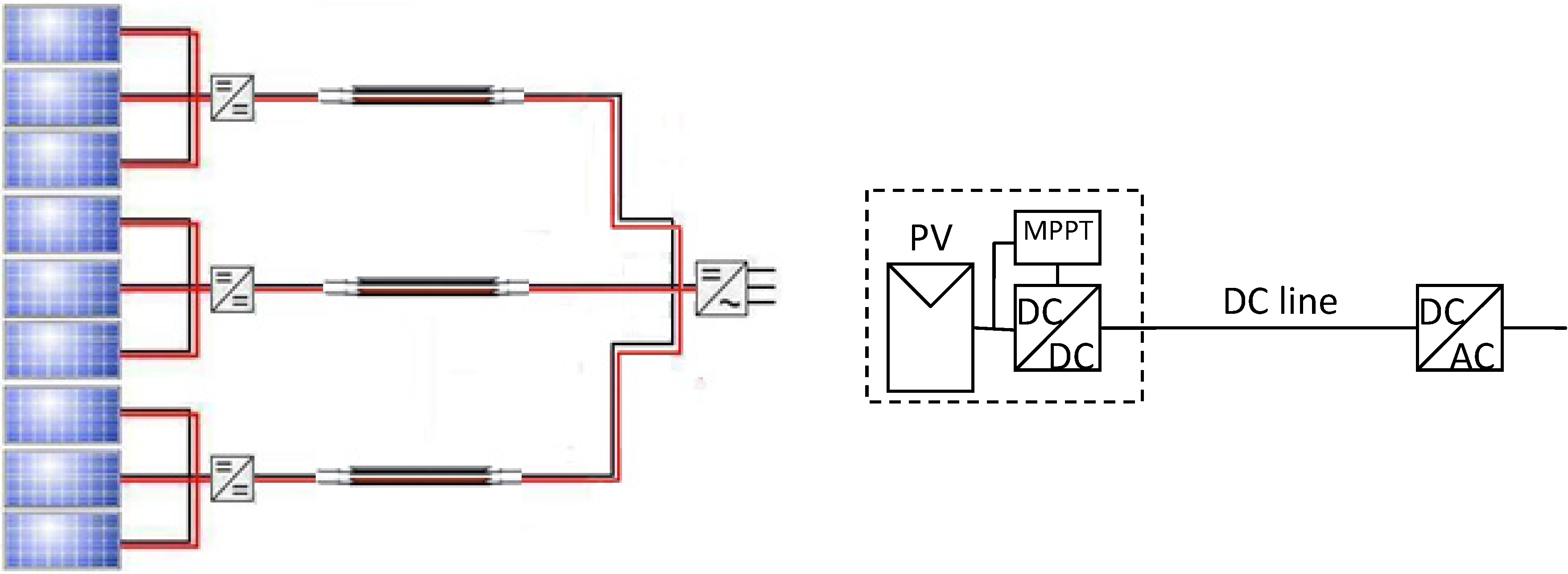
In this paper, a large size PV plant with three strings in parallel has been considered in two different grid configurations. The first configuration, shown in
Figure 1, represents the proposed distributed layout (F) where the DC/DC converters are placed close to each PV string and upstream of the DC cable. The second configuration, shown in
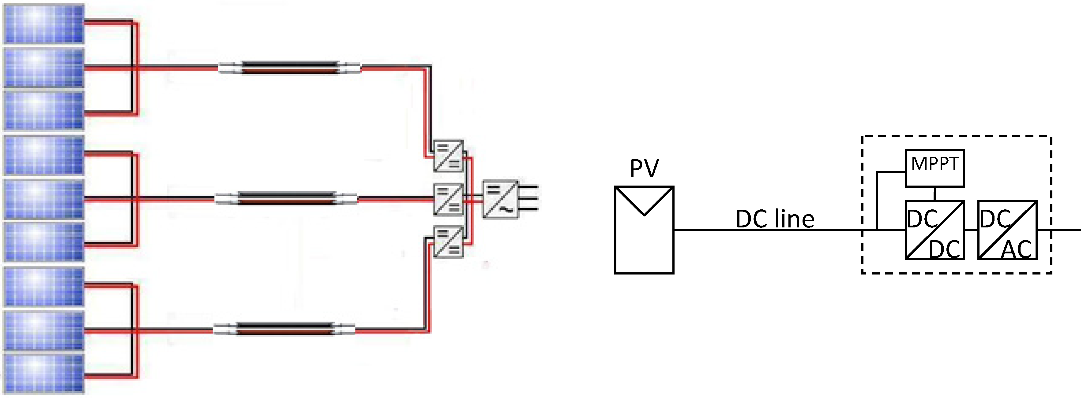
Figure 2, is the concentrated layout (D) where the DC/DC converters are installed near the DC/AC inverter and downstream the DC distribution grid. The major difference between the two configurations is the location of the DC/DC boost converters, while the control logic of the various converters remains the same.
Figure 1.
Layout of PV plant with double-stage separated conversion [(F) configuration].
Figure 1.
Layout of PV plant with double-stage separated conversion [(F) configuration].
Figure 2.
Layout of PV plant with double-stage concentrated conversion ((D) configuration).
Figure 2.
Layout of PV plant with double-stage concentrated conversion ((D) configuration).
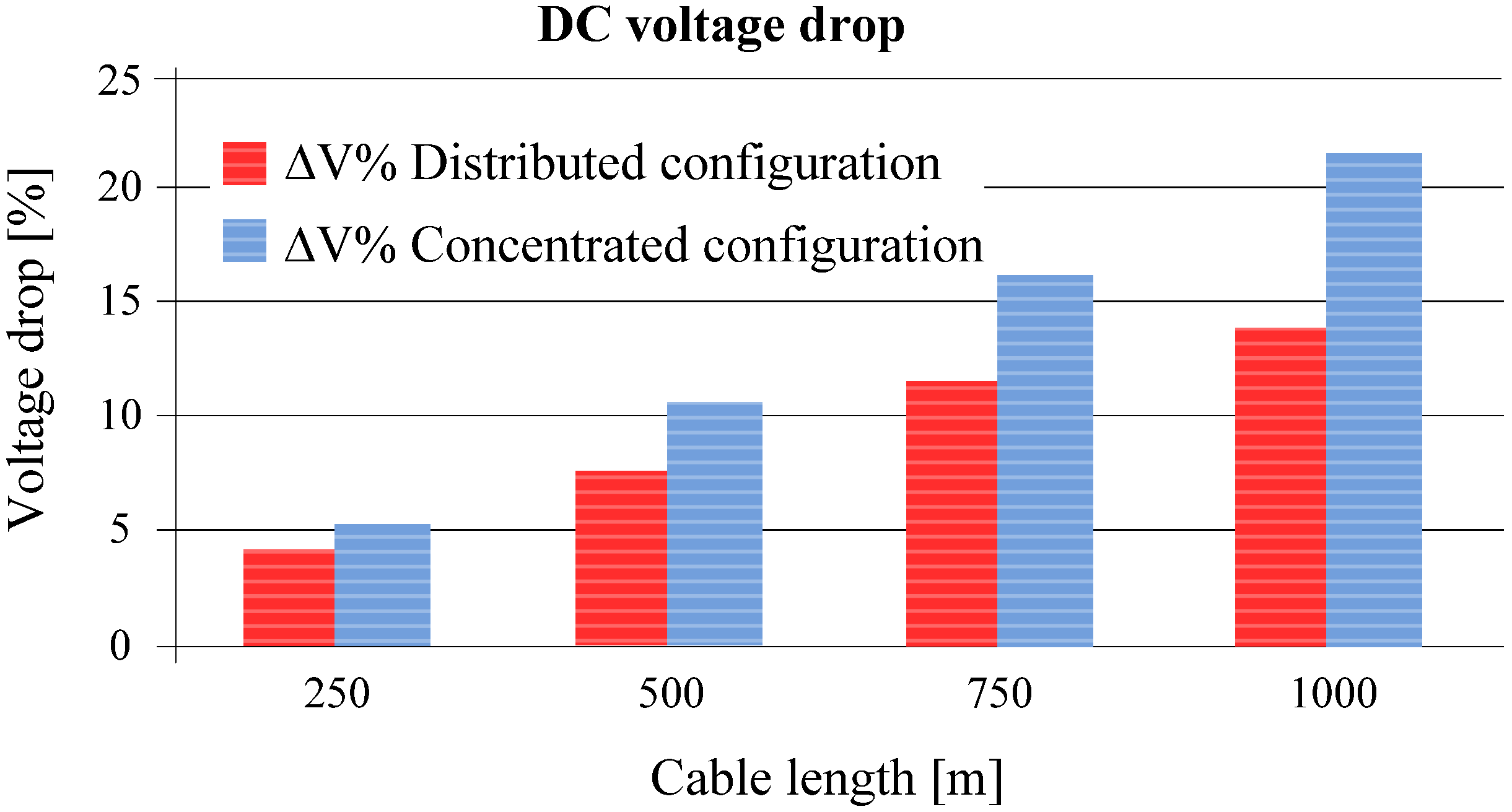
Table 2 reports the main parameters of the considered system. The conducted simulations investigate the voltage drop in the DC grid to evaluate the efficiency of DC distribution system. For a DC cable, characterized by the resistance
r, the
p.u. power losses are equal to the
p.u. voltage drop and can be expressed as:
For each configuration, the voltage drop along the DC cable lines is evaluated as a function of cable length,
i.e., the distance between the PV panels and the grid-connected inverter. The power generated by the PV array is considered constant. The simulation results are illustrated in
Figure 3. From the simulation results shown in
Figure 3, it can be seen that the voltage drop, and hence the power losses, are always lower in the proposed distributed configuration (F) than in the concentrated configuration (D). The results reveal that, in concentrated configuration (D), the power losses in the DC grid increase linearly with the cable length, because the absorbed current by the DC/DC boost converters is constant.
Table 2.
Main parameters for the PV system used in the simulation.
Table 2.
Main parameters for the PV system used in the simulation.
| Parameters | Value |
|---|
| Rated power (kW) | 80 |
| DC distribution voltage (V) | 700 |
| PV string voltage (V) | 500 |
| Cable cross section (mm2) | 16 |
| Cable resistance (Ω/km) | 1.21 |
Figure 3.
Voltage drop along the DC cable for the proposed distributed layout (F) and for the concentrated architecture layout (D), function of cable length.
Figure 3.
Voltage drop along the DC cable for the proposed distributed layout (F) and for the concentrated architecture layout (D), function of cable length.
In the distributed configuration (F), the DC/DC boost converter output voltage increases with the cable length due to the DC voltage drop and because the inverter input voltage is kept constant by its control logic. Hence, the injected current in the DC grid decreases because the output power is constant. Therefore, the power losses and voltage drop are less then linearly dependent on the cable length.
The efficiency of the analyzed configurations is affected by the different locations of the measurements delivering the inputs for the MPPT algorithm. In the concentrated configuration (D), the measurements are undertaken downstream of the DC line. The algorithm does not optimize the energy produced by the PV, but considers the set composed by the PV and DC line. In this case, the optimization of each objective (maximum PV energy and minimum cable losses) cannot be achieved. In the proposed distributed configuration (F), each objective can be optimized separately. The energy produced by the PV is maximized by the MPPT algorithm, while the cable power losses are minimized through a suitable cable design [
16] and keeping the DC voltage as high as possible.
In the distributed configuration, the higher DC voltage allowed by the DC/DC converters, and consequently the lower current, decreases the power losses and the voltage drop. In the concentrated architecture the distribution voltage is smaller and variable as a function of the temperature, solar radiation and the available power.
Another important conclusion of the steady state analysis is that the advantages of a distributed configuration are greater for large and extended power plants (>100 kW) than smaller ones. This is also intuitive because many small concentrated plants tend to a large distributed one. It is possible to conclude that the distributed architecture allows a better exploitation of the solar energy especially in large power plant characterized by different irradiation of the PV panels.
4. Leakage Currents to the Ground and Protection Systems
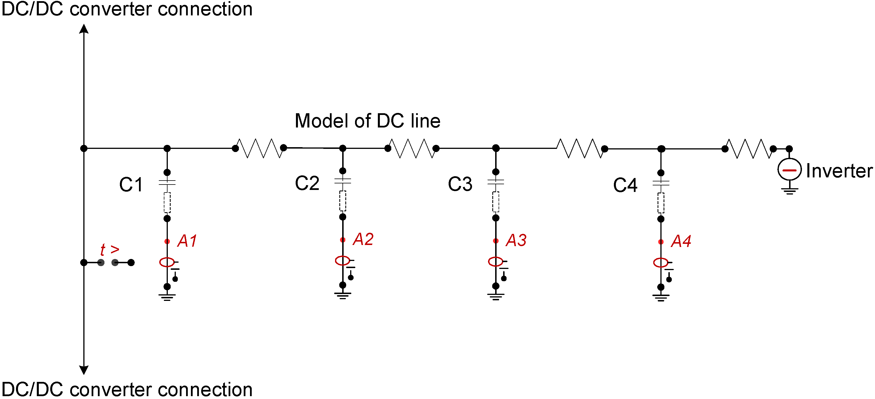
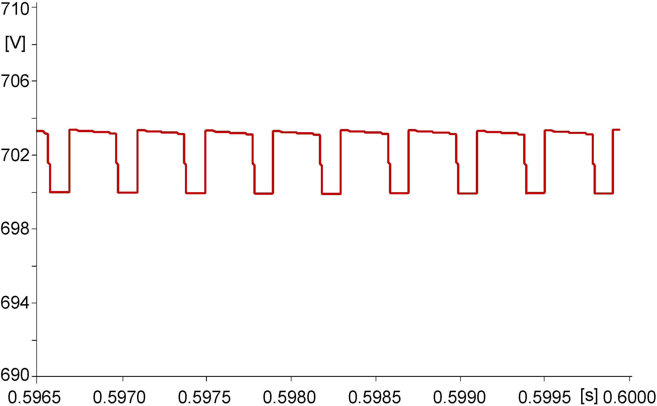
The PV system was modeled using the EMTP‑ATP software. The model considers two or more DC/DC boost converters, a DC distribution grid, and one grid-connected DC/AC inverter. The DC cable is modeled using the series and shunt parameters to evaluate the current drawn to the ground due to the converter switching. The model has been improved step by step to reach a more realistic configuration. A first model considers the DC cable downstream the DC/DC boost converter and upstream the inverter characterized by its resistance Rline = rline∙Lline. To size the cable cross-section, the line current as a function of the characteristics and number of DC/DC boost converters for the settled DC voltage of 700 V must be determined.
The total power of the considered DC/DC boost converters is 80 kW and the line current is 114.3 A. The cable cross-section is 35 mm
2 and the resistance is
rline = 0.55 Ω/km. In case of a cable with a length of 500 m (
Rline = 0.275 Ω) and a 80 kW DC/DC boost converter connected at the beginning of the cable, the waveform of DC line voltage at the converter output is shown in
Figure 4.
Figure 4.
Variation of DC voltage for a cable with a length of 500 m, in proximity of the steady-state condition.
Figure 4.
Variation of DC voltage for a cable with a length of 500 m, in proximity of the steady-state condition.
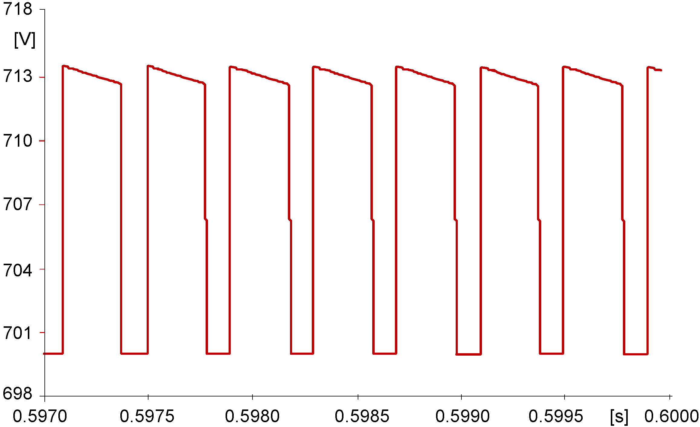
Voltage waveform has trapezoidal shape with amplitude between 700 V and 703 V. These oscillations appear due to the influence of DC cable. The DC cable is not affecting the inverter’s voltage as its value is constant and fixed by the inverter itself. Changing the line length (
lline = 2 km and hence
Rline = 1.1 Ω), the variation of DC line voltage is illustrated in
Figure 5. As it can be observed, the voltage variations have higher amplitude due to the larger voltage drops. The voltage and current harmonics drawn to ground through the capacitances are evaluated. Two DC/DC boost converters operating at different switching frequencies are considered. The case studied is shown in
Figure 6. Every DC/DC boost converter realizes the DC/DC conversion in order to adapt the PV voltage to the DC voltage, exploiting the maximum power available from the PV system.
Figure 5.
Variation of DC voltage for a cable with a length of 2 km, in proximity of the steady-state condition.
Figure 5.
Variation of DC voltage for a cable with a length of 2 km, in proximity of the steady-state condition.
Figure 6.
EMTP/ATP implementation of the case studied, with line models based on π circuit.
Figure 6.
EMTP/ATP implementation of the case studied, with line models based on π circuit.
4.1. Two DC/DC Boost Converters of 40 kWp Each, Interfaced to the 500 m DC Line Through 150 m Long Cables
The simulations consider a DC bus main connection represented through the π model, in which the longitudinal parameter is the resistance and the transversal one is the capacitance with the relative resistance in series. The adopted values are reported in
Table 3.
Table 3.
Main parameters for each DC/DC boost converter and for the DC bus.
Table 3.
Main parameters for each DC/DC boost converter and for the DC bus.
| Parameter | Value |
|---|
| PI controller proportional gain kp | 0.09 |
| PI controller integral gain ki | 1.7 |
| Switching frequency fsw | 2000 |
| Switching inductance L (mH) | 60 |
| DC/DC boost converter’s cable length lcable_converter (m) | 150 |
| DC Bus parameters |
| Resistance Rcable_DC/DC boost converter (Ω) | 0.1815 |
| Line length lline (m) | 500 |
| Resistance Rline (Ω) | 0.275 |
| Line capacitance cline (pF/m) | 277 |
| Capacitance Cline (μF) | 0.138 |
The variation of DC line voltage is shown in
Figure 7, while
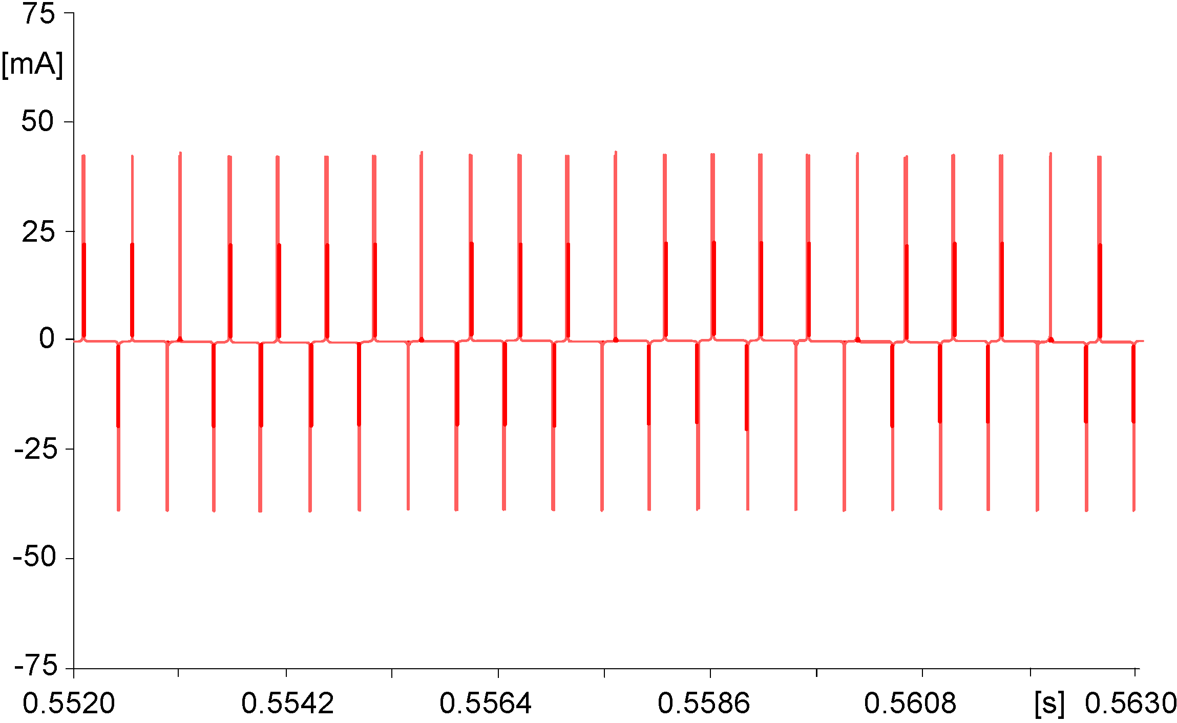
Figure 8 illustrates the variation of the current drawn to ground through the capacitance
C1. This represents the worst case, as
IC1 is the capacitive current that is the most influenced by the vicinity of the DC/DC boost converter.
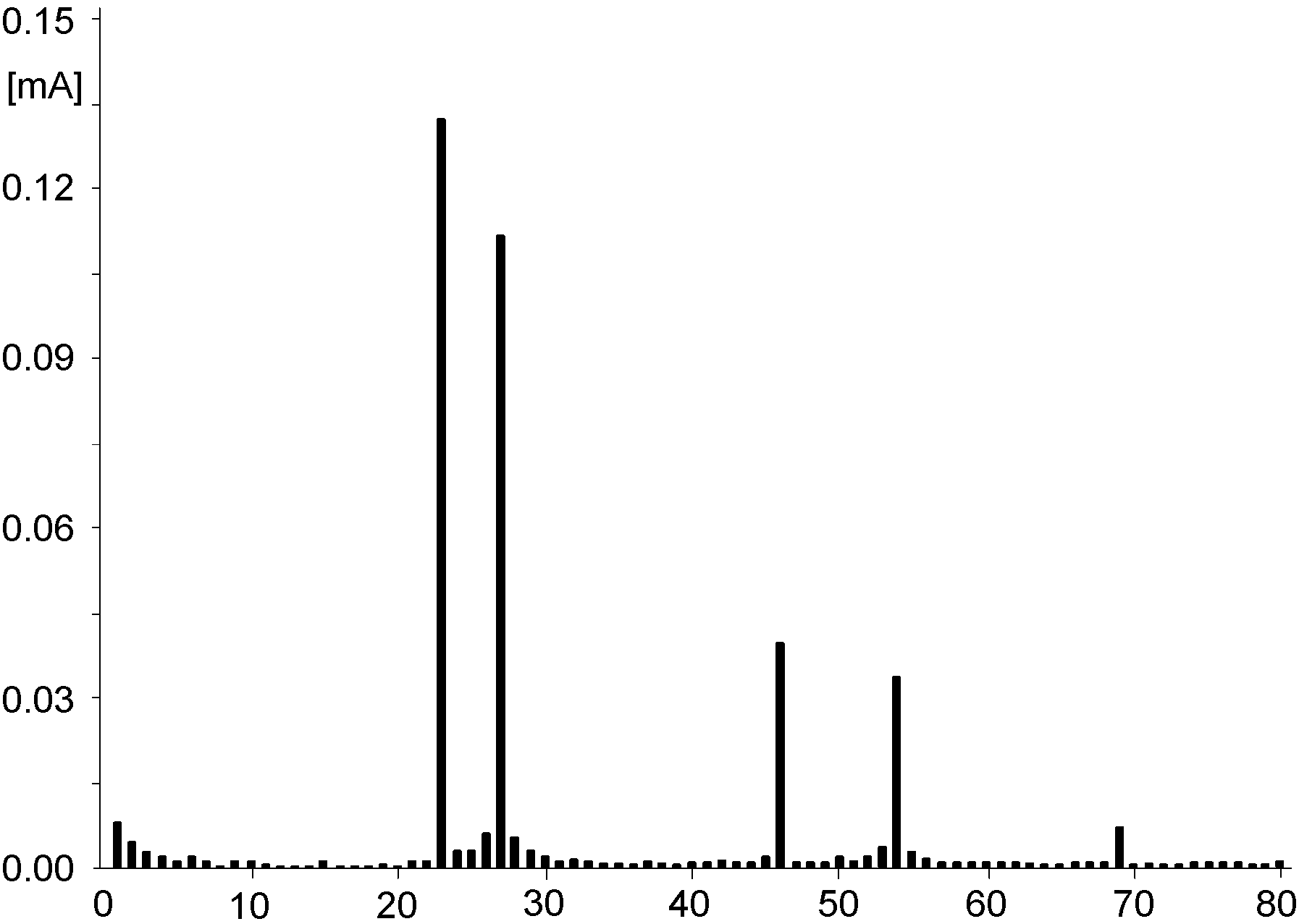
The voltage oscillations are 7 V, while the currents drawn to ground do not exceed 50 mA. The high frequency currents can generate malfunctions of the system differential relays. The DC line voltage is composed of the DC component and harmonics which can interfere with the telecommunication systems. The most relevant harmonics are the tenth (20,000 Hz), the twentieth (40,000 Hz) for the considered converter with 2 kHz switching frequency. Performing the same analysis on the capacitive currents, the highest value founded, considering the current IC1, is 1.4 mA.
Figure 7.
Variation of DC voltage.
Figure 7.
Variation of DC voltage.
Figure 8.
Variation of the current drawn to ground through the capacitance C1.
Figure 8.
Variation of the current drawn to ground through the capacitance C1.
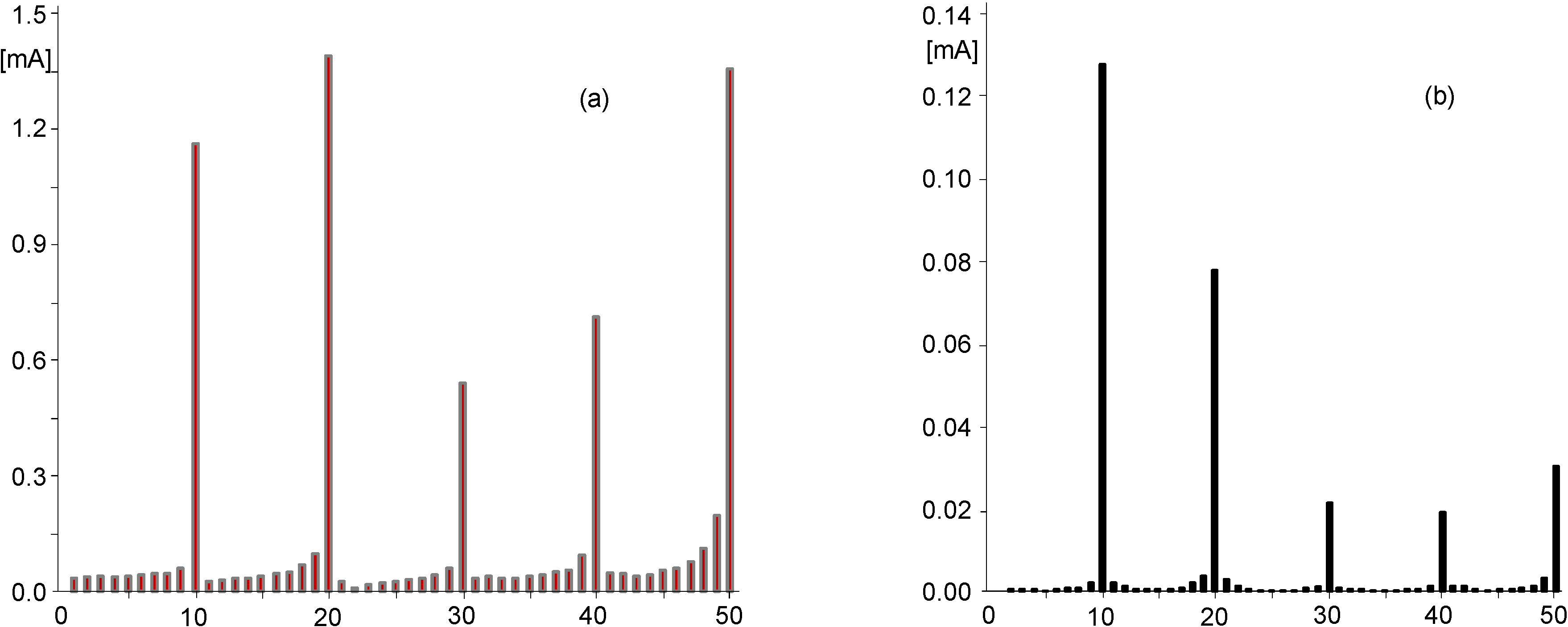
A possible solution to reduce the voltage and current harmonics amplitude is to install an RC filter after the DC/DC boost converter, but before the DC line. For example, simulating the filter insertion, the harmonic at 2000 Hz, that was equal to 2.8 V (without filter), is now equal to 0.30 V. Therefore the voltage behavior will be less rugged (performing the differential protections functioning) but it will have a slower dynamic due to the capacitance introduced that affects the time constant of the system. In
Figure 9, a comparison between the
C1 current spectrum without (
Figure 9a) and with (
Figure 9b) filter is reported. Considering the high frequency currents drawn to ground through the line capacitors, it is possible to conclude that the RC filters use after the DC/DC boost converters improves the situation with less problems for the differential protections.
Figure 9.
(a) The C1 current spectrum without filter; (b) The C1 current spectrum with filter.
Figure 9.
(a) The C1 current spectrum without filter; (b) The C1 current spectrum with filter.
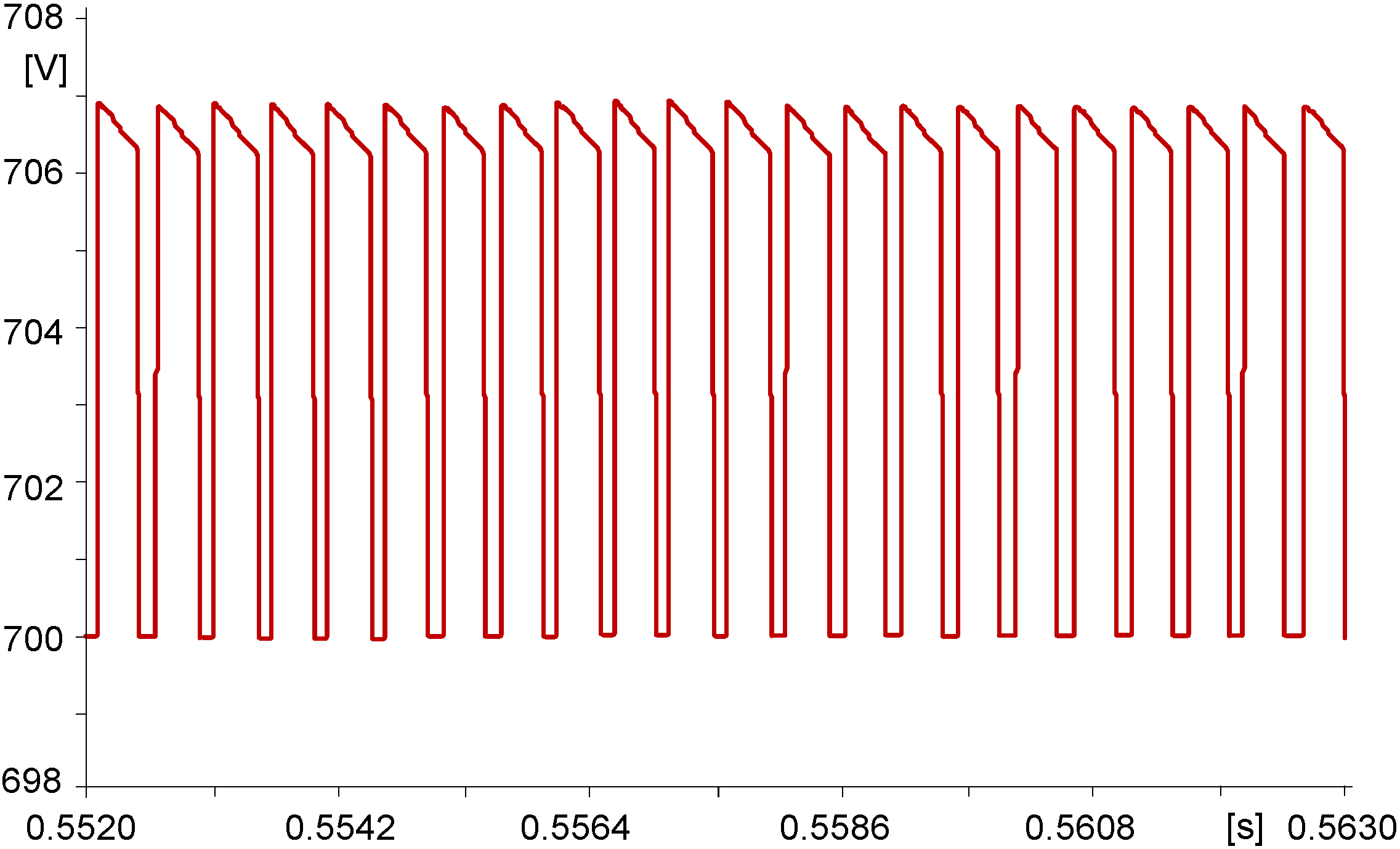
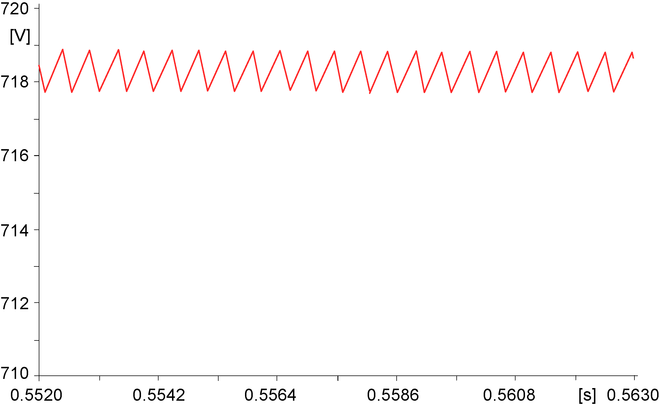
4.2. Two DC/DC Boost Converters of 40 kWp Each, Interfaced to the 2 km DC Line through 150 m Long Cables
The following simulations consider the values reported in
Table 4. It is easy to note in
Figure 10 that the peak value of the DC line voltage is higher than the previous case (706 V for
l = 500 m; 718 V for
l = 2000 m) but the oscillation are minor thank to the filters introduction. Consequently, the currents drawn to ground through the capacitances are less.
Table 4.
Main parameters for each DC/DC boost converter and for the DC bus.
Table 4.
Main parameters for each DC/DC boost converter and for the DC bus.
| Parameter | Value |
|---|
| PI controller proportional gain kp | 0.09 |
| PI controller integral gain ki | 1.7 |
| Switching frequency fsw | 2000 |
| Switching inductance L (mH) | 60 |
| DC/DC boost converter's cable length lcable_converter (m) | 150 |
| Resistance RcableDC/DC boost converter (Ω) | 0.1815 |
| DC Bus parameters |
| Line length lline (m) | 2000 |
| Resistance Rline (Ω) | 1.1 |
| Line capacitance cline (pF/m) | 277 |
| Capacitance Cline (μF) | 0.554 |
Figure 10.
DC line voltage (two parallel DC/DC boost converters).
Figure 10.
DC line voltage (two parallel DC/DC boost converters).
Performing the same frequency analysis of the previous case, the harmonics in the voltage waveform are at the switching frequency of the two converters and at their multiples. The amplitude values are increased due to the longest line that means higher values of the DC/DC boost converter voltage and, therefore, higher harmonics amplitude. The same is for the currents drawn to ground through the capacitances. The value of the tenth harmonic is now 0.66 mA (respect to the 0.21 mA of the previous case). In conclusion, it is possible to deduce that the most the voltage oscillates (closest to the DC/DC boost converter), the highest is the value of the current drawn to ground and therefore its harmonics.
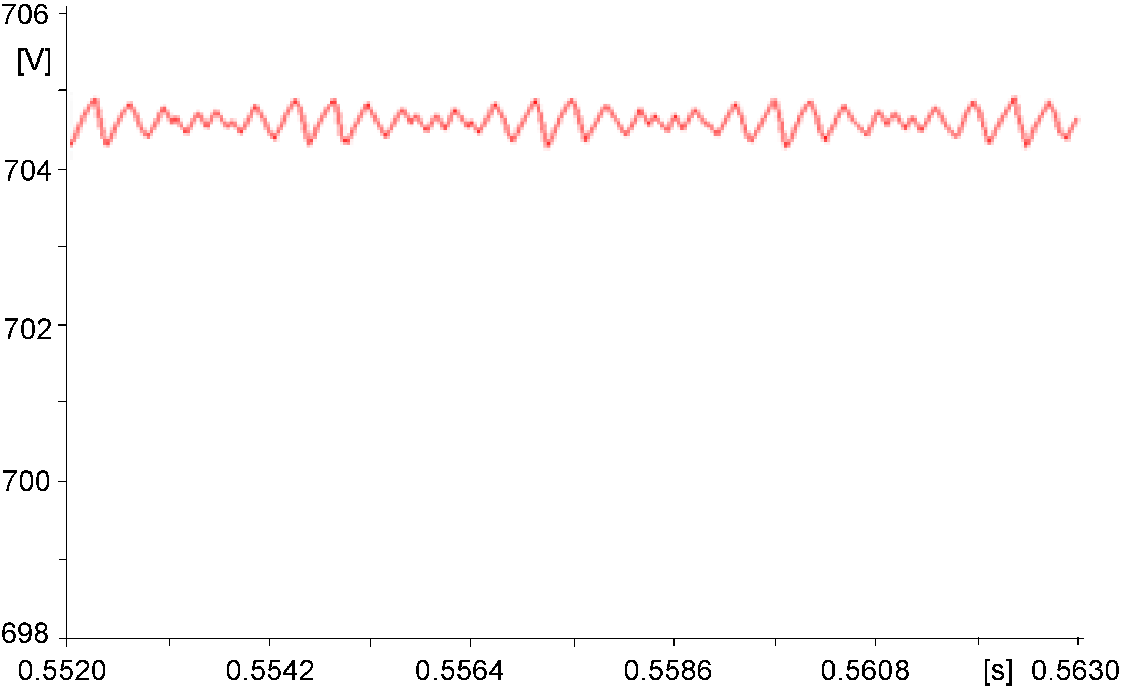
4.3. Two DC/DC Boost Converters of 40 kWp Each, with Different Switching Frequencies, Interfaced to the 2 km DC Line through 150 m Long Cables
The following simulations consider the values reported in
Table 5. It is interesting to observe what happens if the switching frequencies of the two DC/DC boost converters is not the same. In order to consider the most general case, two not multiple frequencies are chosen. Always for synthesis reason, only the case with filters is here reported. The adopted values are reported in the following.
Table 5.
Main parameters for each DC/DC boost converter and for the DC bus.
Table 5.
Main parameters for each DC/DC boost converter and for the DC bus.
| Parameter | Value |
|---|
| PI controller proportional gain kp | 0.09 |
| PI controller integral gain ki | 1.7 |
| Switching frequency DC/DC boost converter #1 fsw | 2300 |
| Switching frequency DC/DC boost converter #2 fsw | 2700 |
| Switching inductance L (mH) | 60 |
| DC/DC boost converter's cable length lcable_converter (m) | 150 |
| Resistance Rcable_DC/DC boost converter (Ω) | 0.1815 |
| DC Bus parameters |
| Line length lline (m) | 500 |
| Resistance Rline (Ω) | 0.275 |
| Line capacitance cline (pF/m) | 277 |
| Capacitance Cline (μF) | 0.138 |
The DC line voltage and the capacitive currents to ground behaviors have strong deformations in their waveforms (
Figure 11 and
Figure 12). This is due to the different switching frequency of the converters that leads to beating frequencies that distorter the signal.
Figure 11.
DC line voltage (two parallel DC/DC boost converters).
Figure 11.
DC line voltage (two parallel DC/DC boost converters).
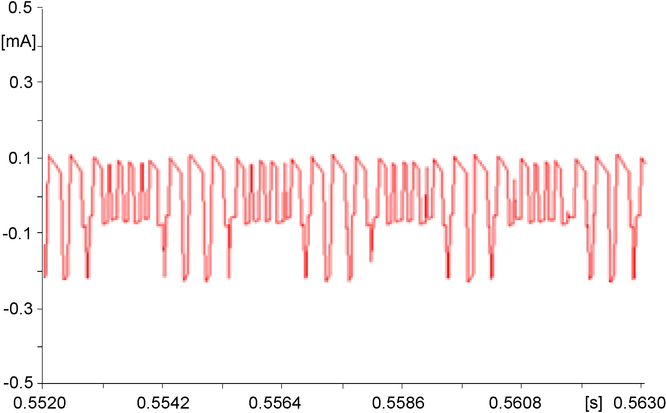
Figure 12.
Current drawn to ground through the capacitance C1.
Figure 12.
Current drawn to ground through the capacitance C1.
The voltage is constituted by a DC component equal to 704 V and a harmonics series. The frequency considered for the frequency analysis is 100 Hz (
Figure 13).
Figure 13.
DC line voltage spectrum (two parallel DC/DC boost converters).
Figure 13.
DC line voltage spectrum (two parallel DC/DC boost converters).
The highest harmonics are the 23th and the 27th that are the switching frequencies and their influence decreases with the growth of the harmonic order. Regarding the capacitive currents, their harmonic values are very low due to the filter insertion.
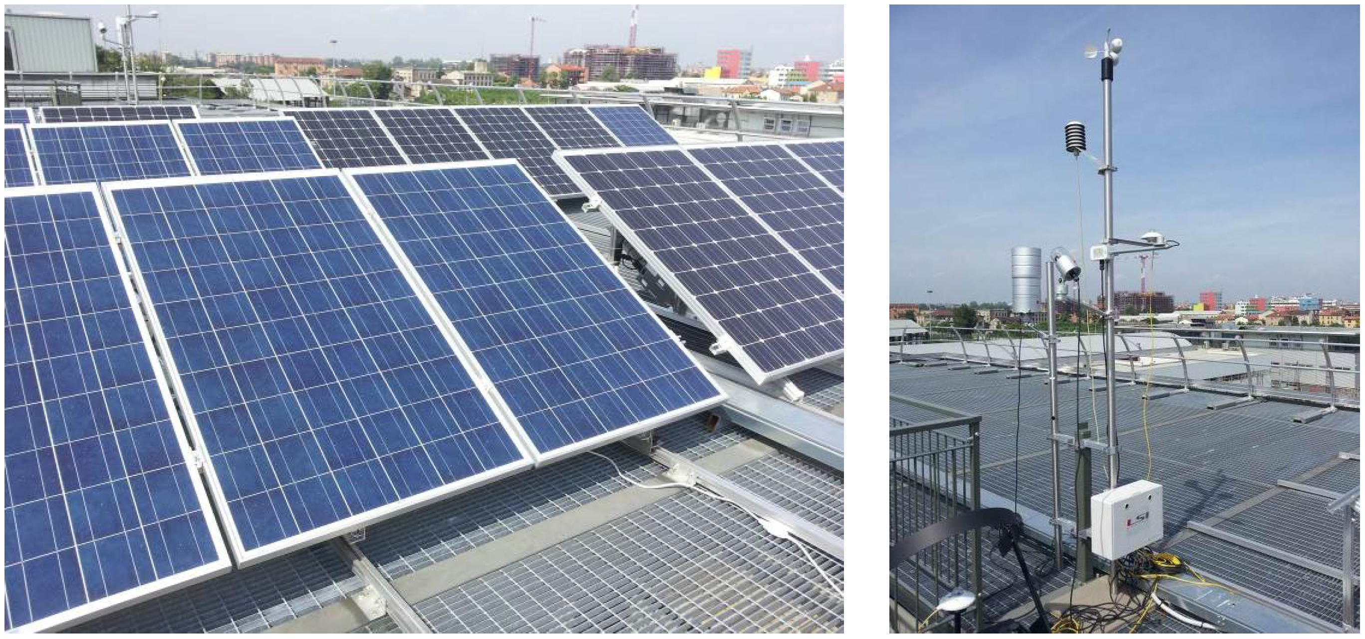
5. Experimental Results
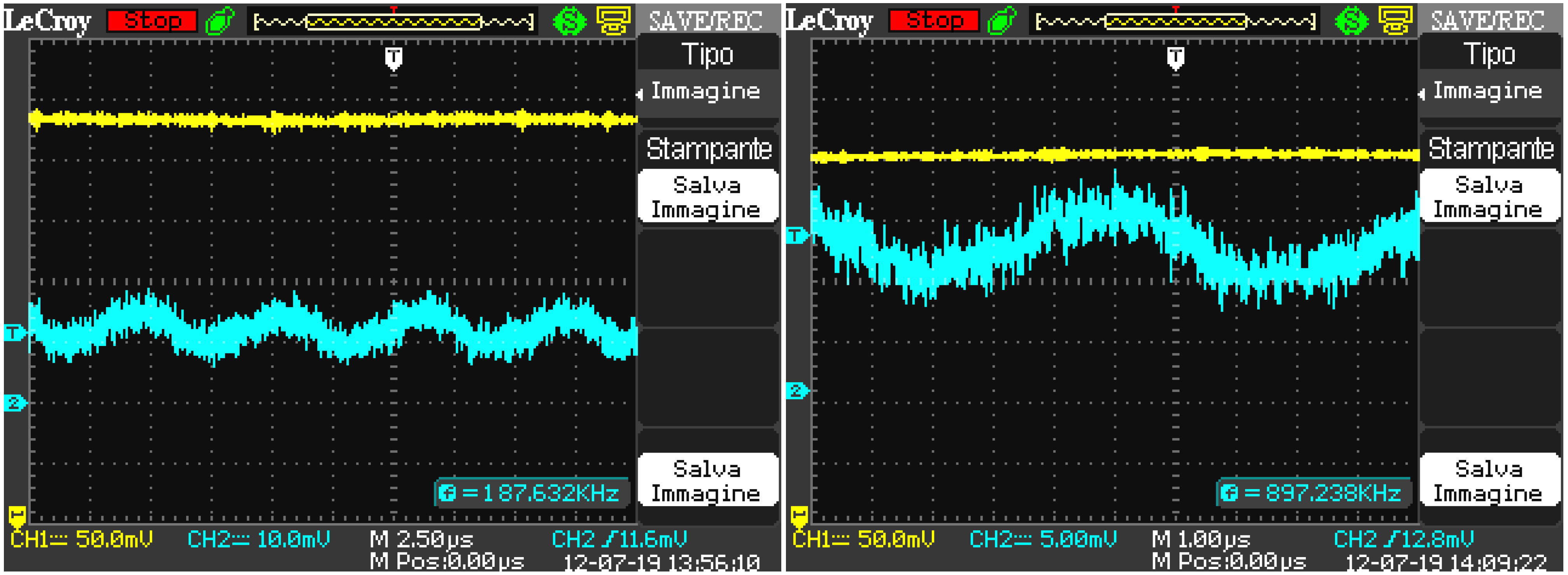
The theoretical analysis above described has been tested on a small-scale prototype available in the Solar Tech laboratory of the Politecnico di Milano equipped with different PV module typologies. A picture of the employed system is reported in
Figure 14a, while
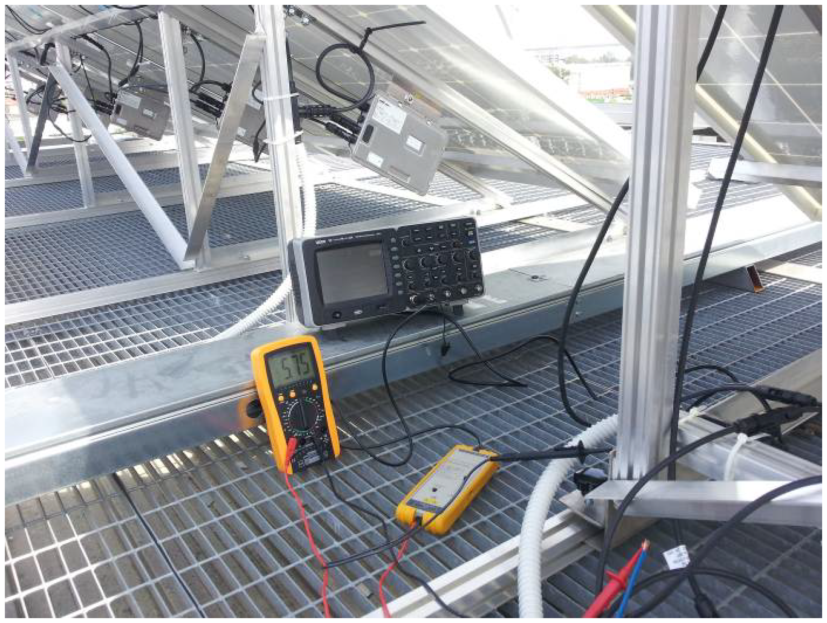
Figure 14b represents the weather station. The DC/AC converter employed in this study is constituted by an input DC/DC stage that performs the MPPT, a middle stage with high frequency transformer for network insulation, a bulk capacitor and an output DC/AC stage. The PV prototype system has been tested in a clear sunny day with an oscilloscope and a voltage and current probes (
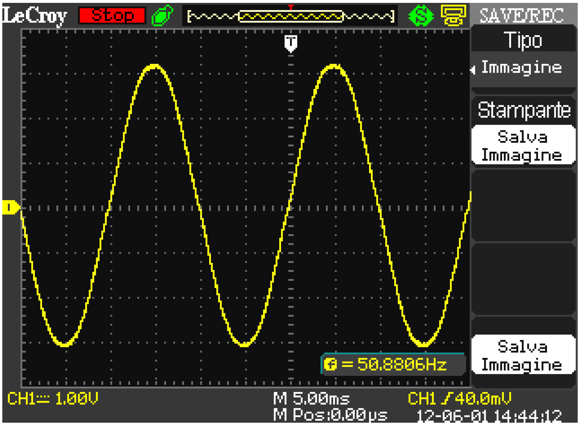
Figure 15). The PV arrays generate DC current equal to 5.75 A and it has been interfaced to the AC distribution system in pure sinusoidal voltage condition (
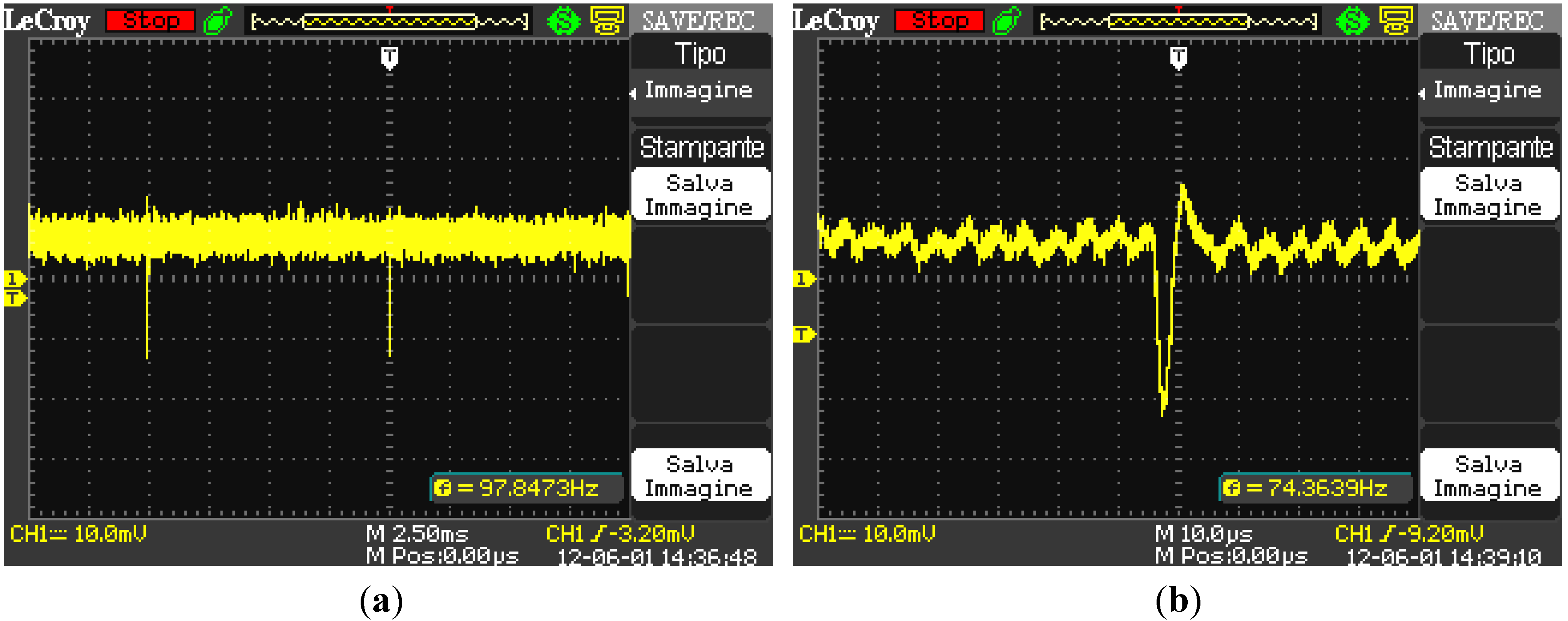
Figure 16). In particular the DC voltage respect to the ground has been measured (
Figure 17a). The carried out measurements confirm the above simulations in which repetitive spikes are overlapped to the DC ripple due to the inverter switching. In particular, a zoom of the spikes is depicted in
Figure 17b.
Figure 14.
(a) Solar Tech Lab of the Politecnico di Milano, Italy; (b) Weather station of the Solar Tech Lab.
Figure 14.
(a) Solar Tech Lab of the Politecnico di Milano, Italy; (b) Weather station of the Solar Tech Lab.
Figure 15.
Measurement setup of the DC current generated by the PV arrays.
Figure 15.
Measurement setup of the DC current generated by the PV arrays.
Figure 16.
Input AC sinusoidal voltage.
Figure 16.
Input AC sinusoidal voltage.
Figure 17.
(a) Positive pole to ground voltage; (b) Particular of the DC voltage spikes.
Figure 17.
(a) Positive pole to ground voltage; (b) Particular of the DC voltage spikes.
The experimental measurements confirm that transient phenomena can occur in the floating DC section and in more powerful PV plant they can cause untimely trip protection or other disturbances in the main system.
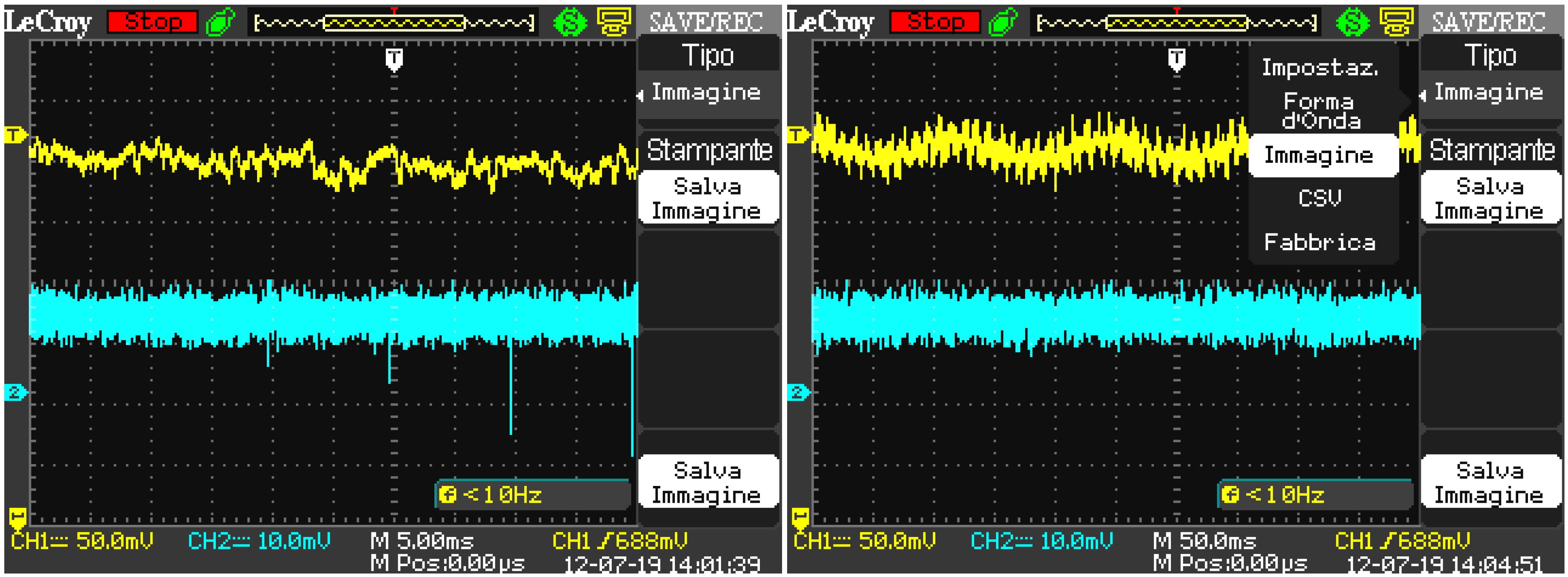
Other measurements have been performed in order to evaluate all the system conditions. Firstly, the DC to ground voltage has been zoomed and compared with the DC current (
Figure 18). As it can be seen, this voltage contains a sinusoidal ripple at 200 kHz mainly due to the natural oscillation frequency between the connection DC cables and the input EMI filter. This oscillation is maintained by the high switching frequency of the DC/DC converter. In this range of frequencies the DC current appears constant.
Subsequently, the DC current variations have been analyzed. In
Figure 19a it is possible to observe a current ripple similar to those one previously simulated and reported in
Figure 12 due to the switching of the input DC/DC stage. Instead,
Figure 19b shows the current oscillation caused by the MPPT algorithm that continues to vary the DC power in order to maintain the maximum power operating point with changing atmospheric conditions.
Figure 18.
(a) DC to ground voltage oscillation (cyan trace) and DC current (yellow trace); (b) Particular of the DC voltage ripple.
Figure 18.
(a) DC to ground voltage oscillation (cyan trace) and DC current (yellow trace); (b) Particular of the DC voltage ripple.
Figure 19.
(a) DC to ground voltage (cyan trace) and DC current (yellow trace); (b) Particular of the DC current oscillation due to MPPT.
Figure 19.
(a) DC to ground voltage (cyan trace) and DC current (yellow trace); (b) Particular of the DC current oscillation due to MPPT.


