1. Introduction
Limited fossil energy and increased air pollution have spurred researchers to develop clean energy sources. One of these sources is the photovoltaic (PV) power generation system, which is a clean, quiet and an efficient method for generating electricity. In practical applications, PV arrays can be used in battery charging, water pumping, PV vehicles, satellite power systems, grid-connected power systems, standalone power systems, and so on. Due to the low conversion efficiency of PV arrays, on way to reduce the cost of the overall system is by using high efficiency power processors. The power processor usually adopts a dc/dc converter as its energy processing system.
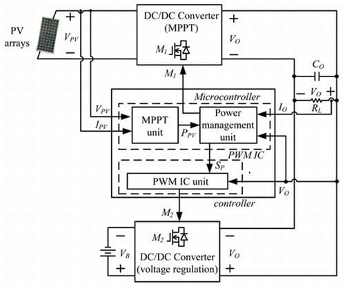
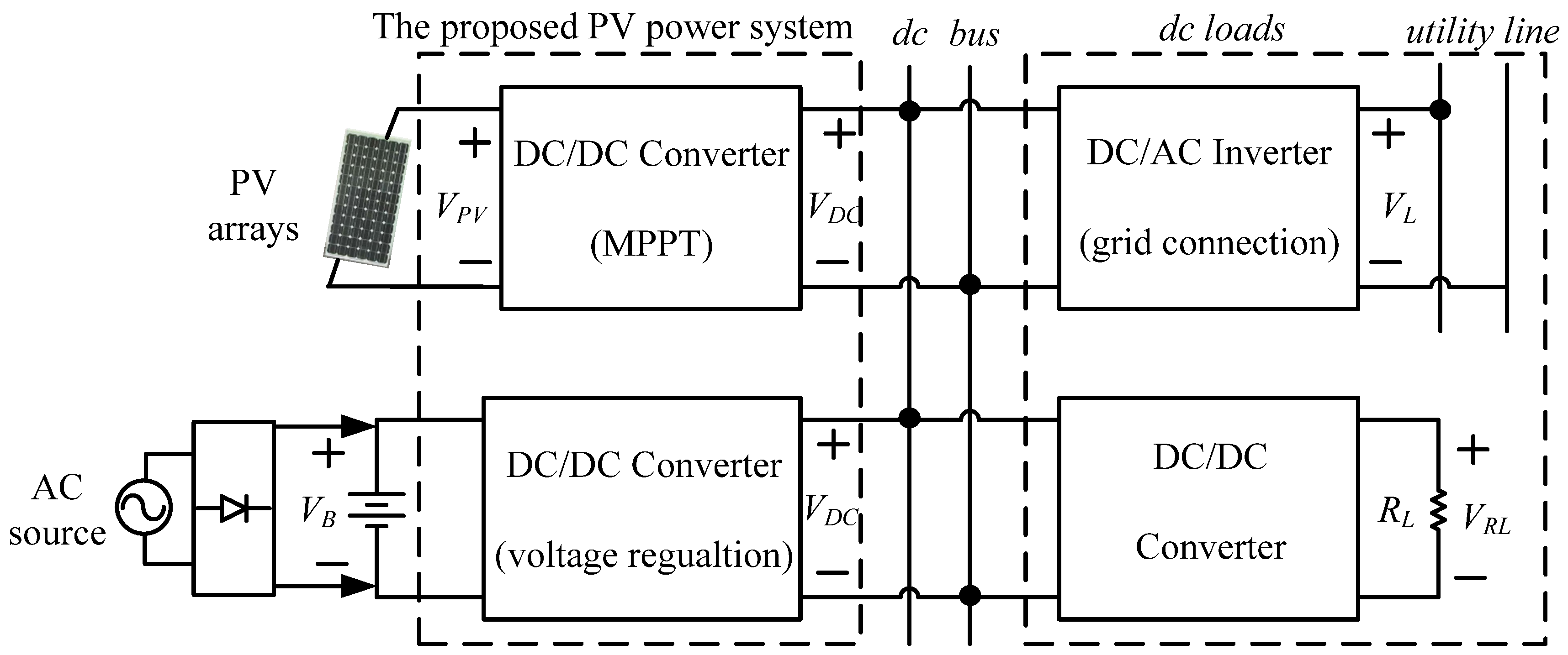
When a dc/dc converter is used in a PV array power system, it is operated at the maximum power point (MPP) of the PV arrays to extract the maximum possible power for increasing the utilization rate of the PV arrays. As a result, its output voltage does not remain at the desired constant dc voltage. Therefore, a dc/dc converter with voltage regulation is used to connect with PV power systems in parallel to keep the output voltage in the desired constant dc voltage range, as shown in
Figure 1.
Figure 1.
Block diagram of PV power generation system for DC load applications.
Figure 1.
Block diagram of PV power generation system for DC load applications.
In
Figure 1, the dc bus voltage can supply a dc/ac inverter for a grid-connected power system [
1,
2,
3,
4,
5], a dc/dc converter for dc load [
6,
7,
8,
9,
10], and so on. The dc/ac inverter and dc/dc converter are regarded as dc loads. In this paper, the proposed power supply includes a dc/dc converter as the maximum power point tracking (MPPT) point of the PV arrays and a dc/dc converter as the load voltage regulator.
To increase the utility rate of PV arrays, power systems using PV arrays must track MPP to extract as much power as possible from the arrays. Several MPPT algorithms have been proposed [
11,
12,
13,
14,
15,
16,
17,
18,
19,
20]. Some of the more popular MPPT algorithms are the constant voltage method [
11,
12], β method [
13], system oscillation method [
14,
15], ripple correlation method [
16], incremental conductance method [
17] and perturb and observe method [
18,
19,
20]. Due to its simplicity and ease of implementation, the perturb and observe method is often used. Therefore, the perturb and observe method was adopted to implement the MPPT of the proposed power system.
In order to increase the conversion efficiency of a PV power system, switching power converters are widely used as dc/dc converters. Since the proposed PV power system requires a high step-up dc/dc converter, a transformer or coupled inductor is usually introduced into switching power converters [
21,
22]. Compared with the converter using an isolation transformer, the one using a coupled inductor has a simpler winding structure and a higher coupling coefficient. It can reduce inductor currents to ensure lower conduction losses and decrease leakage inductance to attain a lower switching loss, respectively. As a result, the one can use a lower value of the input filter capacitor to obtain a good regulation of the output voltage. Therefore, a system using a coupled inductor is relatively attractive. However, since the energy is trapped in the leakage inductor of the coupled inductor, it will not only increase voltage stresses, but induce significant switching losses of the switches in the converter. In order to solve these problems, several methods have been proposed [
23,
24,
25]. In [
23], a resistor-capacitor-diode (R-C-D) snubber is used to alleviate switch voltage stresses, but the energy trapped in the leakage inductor is dissipated by the resistor, resulting in a lower conversion efficiency of the converter. Therefore, a passive losses circuit [
24] is adopted to recover the energy and reduce voltage spikes across switches, but active switches are still operated in hard switching mode. Its conversion efficiency does not increase significantly. In [
25], an active clamp circuit is introduced into the converter for recovering the energy of the leakage inductor and limit voltage spike across switches. Moreover, the one can also achieve zero-voltage switching (ZVS) in converter switches to increase their conversion efficiency. As mentioned above, a boost converter associated with a coupled inductor is adopted in this research as the dc/dc converter, as shown in
Figure 2. In order to further increase the powering capability of the converter, boost converters with interleaved manner have been proposed by several authors [
26,
27,
28,
29], as shown in
Figure 3.
Figure 2.
Schematic diagram of a boost converter with coupled inductor.
Figure 2.
Schematic diagram of a boost converter with coupled inductor.
Figure 3.
Schematic diagram of interleaved active clamp boost converter with coupled inductor.
Figure 3.
Schematic diagram of interleaved active clamp boost converter with coupled inductor.
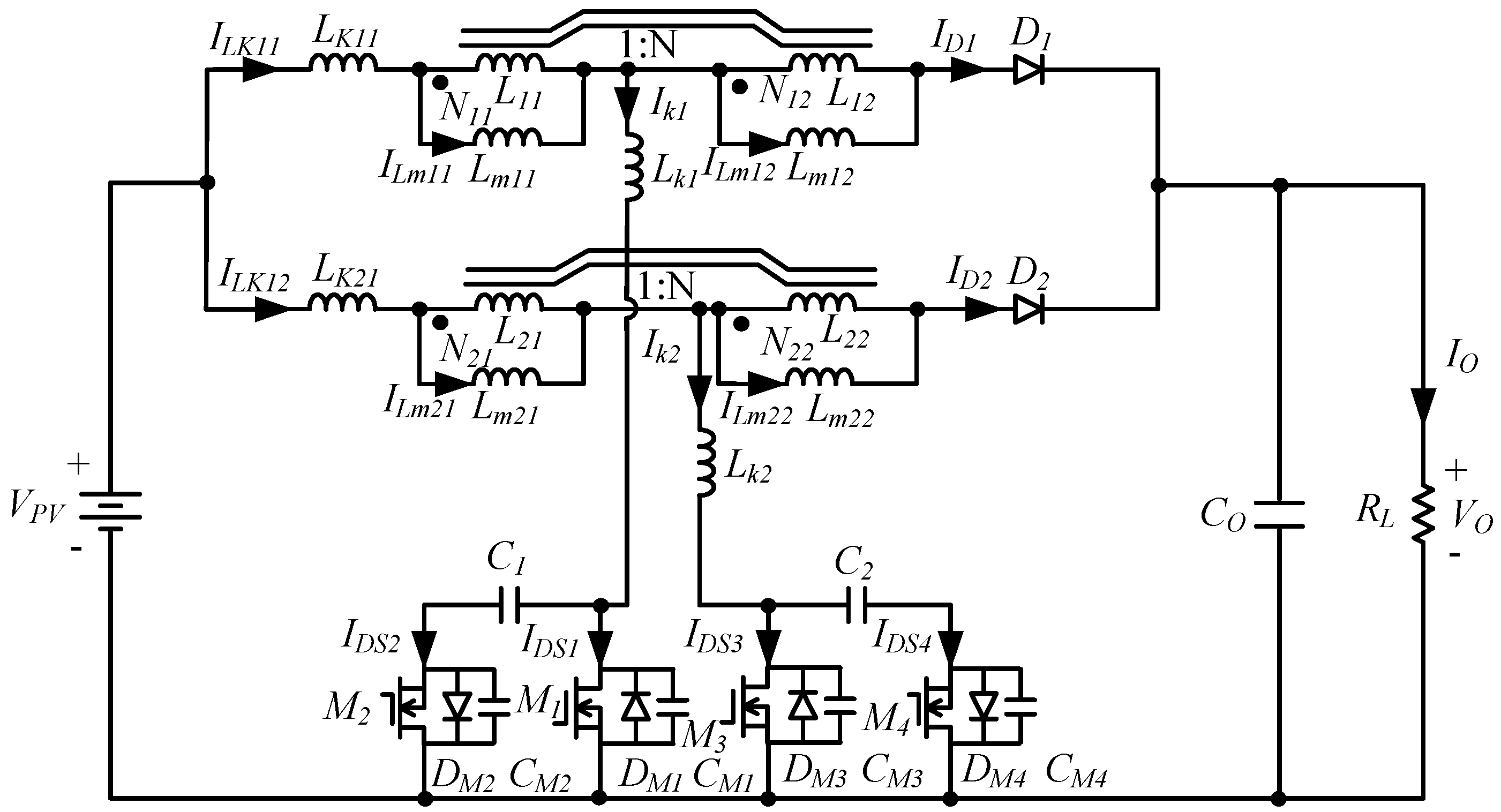
Due to the complexity of the circuit structure, the proposed dc/dc converter can be simplified however, as shown in
Figure 4. From
Figure 4, it can be seen that the proposed interleaved active clamp boost converter can use less component counts to achieve a high step-up voltage ratio and similar conversion efficiency for reducing the costs.
Figure 4.
Schematic diagram of the proposed interleaved active clamp boost converter with coupled inductor.
Figure 4.
Schematic diagram of the proposed interleaved active clamp boost converter with coupled inductor.
In particular, a general half-bridge converter, push-pull converter and full-bridge converter need pulse-width modulation (PWM) IC with two gate signals to drive their switches. Since the input sources of the converters adopt the voltage fed type, the duty ratios of their control PWM ICs are limited to within 0.5. If the dc/dc converter adopts a special PWM IC, which has a higher duty ratio (≥0.5), these are difficult to obtain and the cost will be increased.
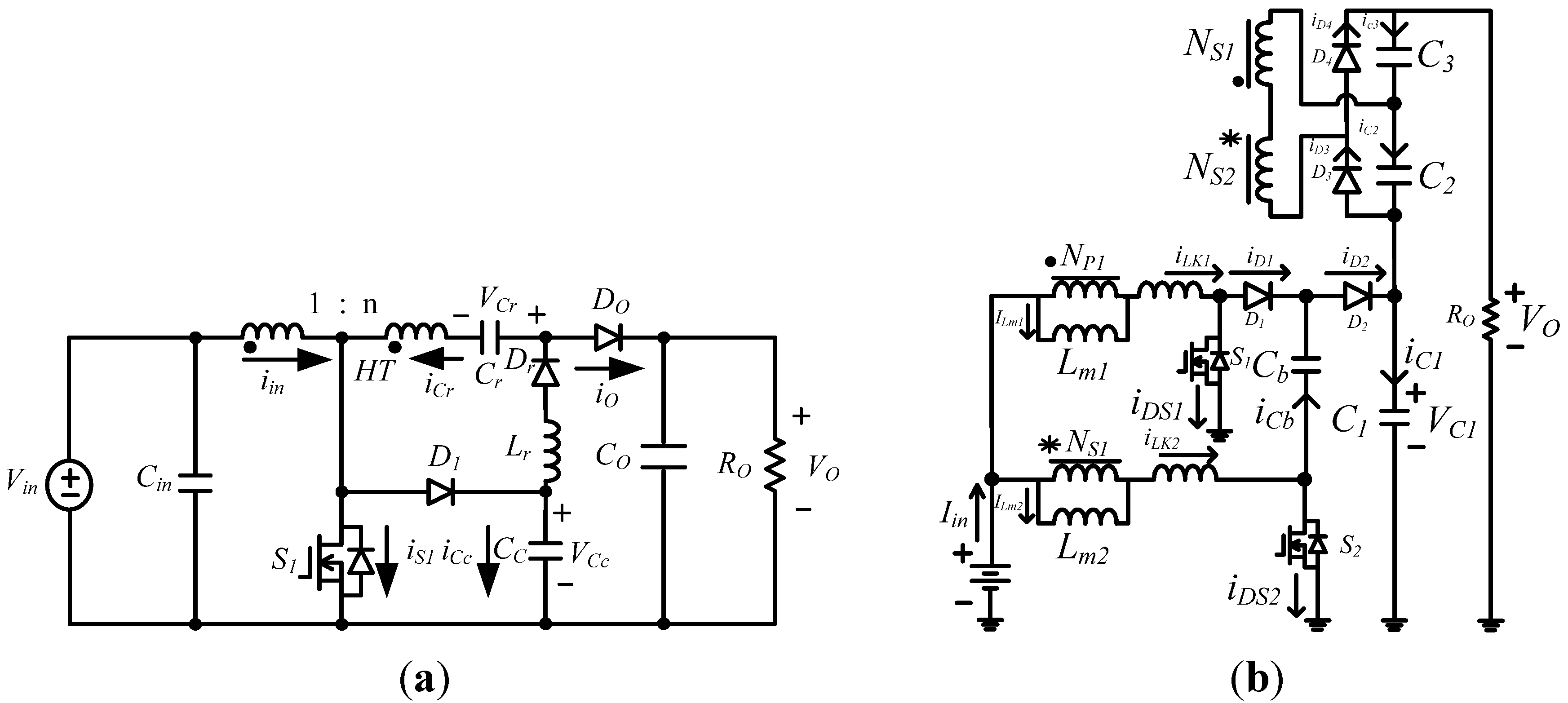
In [
28], as shown in
Figure 5a, the duty ratios of switches in the proposed converters require that the duty ratios of the PWM ICs must be greater than 0.5, resulting in a higher cost. Moreover, its resonant capacitor has a higher current ripple rating (CRR), and it will need a special capacitor, which has a low ESR, high CRR and high operational bandwidth. Therefore, it is suitable for a low power level application. In [
29] a voltage multiplier module to implement a high step-up voltage ratio was proposed, as shown in
Figure 5b. Its voltage doubler capacitors also require a higher CRR. In particular, its controller adopts a DSP to implement its control method. Its cost is increased and its powering capability will be limited. In order to reduce the limitations of PWM ICs and capacitors for a voltage regulator, the proposed dc/dc converter can use a general PWM IC with two gate signals to achieve a high step-up voltage ratio and a high conversion efficiency with less component counts. As mentioned above, the proposed converter can reduce cost and further decrease its size, weight and volume. It is suitable for PV arrays applications when the PWM IC duty ratios are less than 0.5.
Figure 5.
Schematic diagram of the conventional high step-up converters (
a) proposed in [
28]; and (
b) proposed in [
29].
Figure 5.
Schematic diagram of the conventional high step-up converters (
a) proposed in [
28]; and (
b) proposed in [
29].
5. Experimental Results
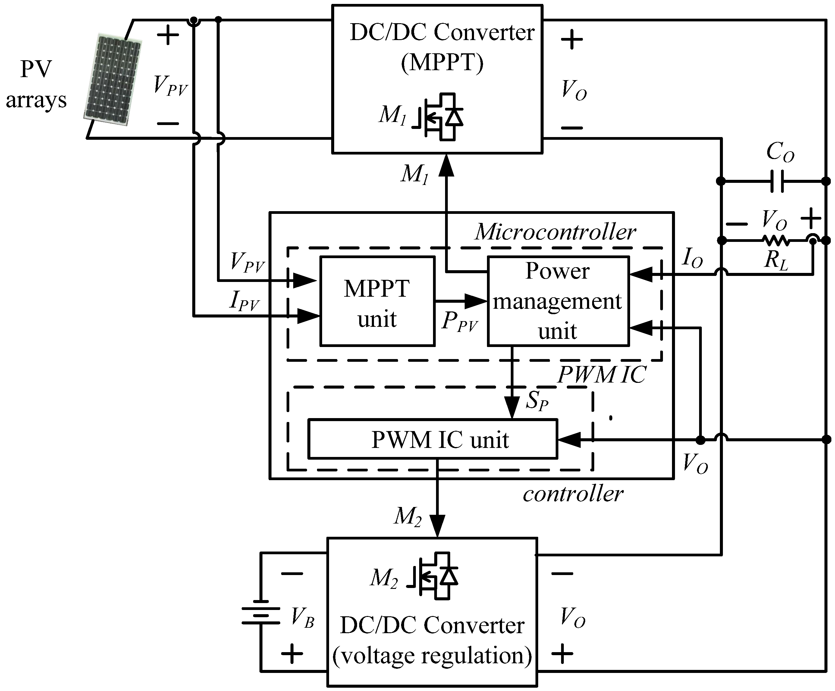
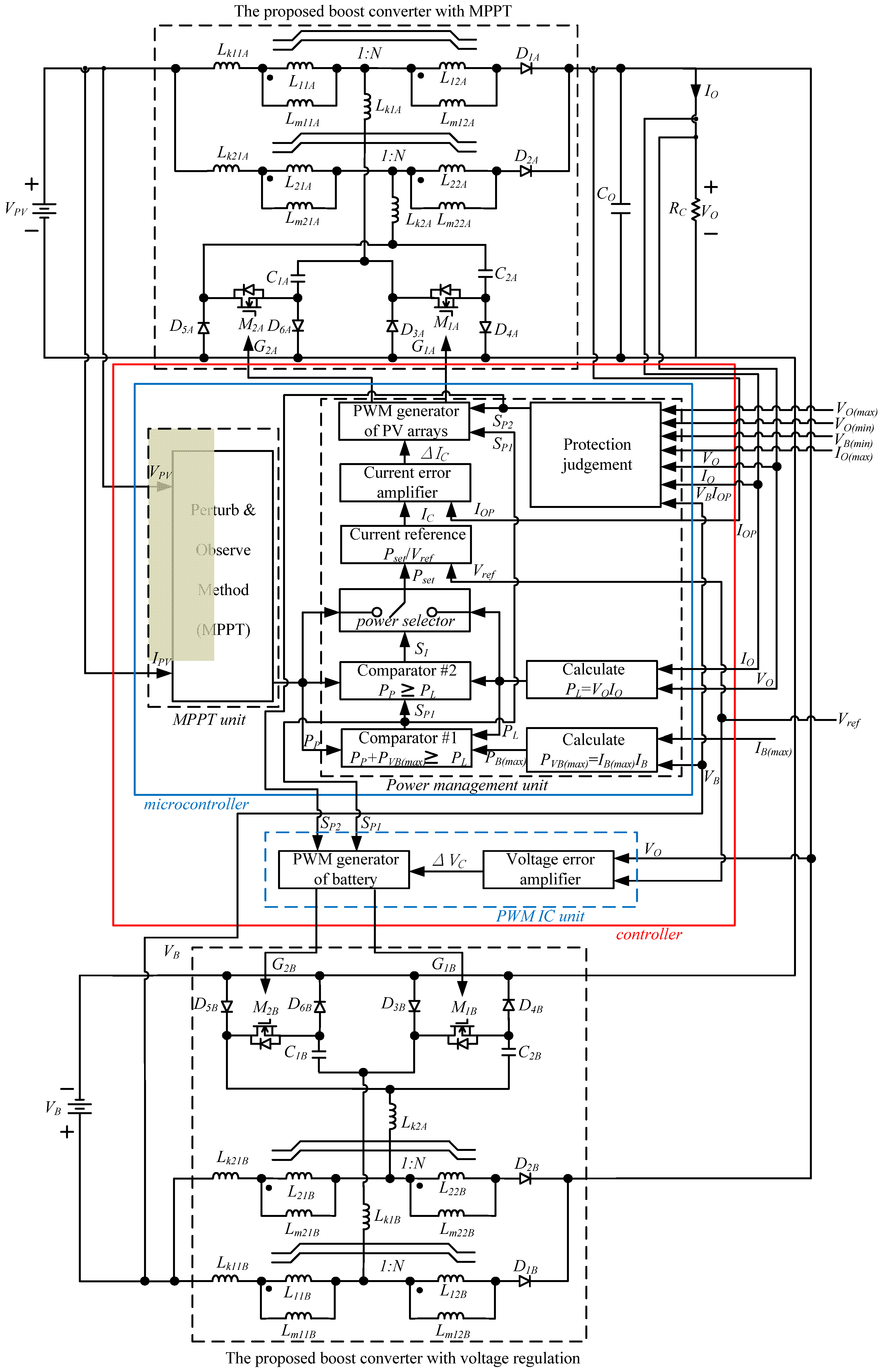
The proposed PV power system is shown in
Figure 13. To verify the performance of the proposed PV power system, two dc/dc converters using an interleaved active clamp boost converter with coupled inductor to generate dc voltage of 400 V for dc load applications with the following specifications were implemented:
The proposed boost converter with MPPT
Input voltage VPV: 34~42 Vdc (PV arrays);
Output voltage VO: 400 Vdc;
Output maximum current IOP(max): 3 A; and
Output maximum power PPV(max): 1.2 kW.
The proposed boost converter with voltage regulation
Input voltage VB: 40~54 Vdc (four sets of 12 V batteries connected in series);
Output voltage VO: 400 Vdc;
Output maximum current IOB(max): 3 A; and
Output maximum power PB(max): 1.2 kW.
According to designs and specifications of the proposed boost converters, components of power stages in the proposed two boost converters are determined as follows:
Switches M1A, M2A, M1B, M2B: IRFP260N×2 (connected in parallel);
Diodes D1A, D2A, D1B, D2B: DSSK60-02A;
Diodes D3A, D4A, D5A, D6A: DSSK60-02A;
Diodes D3B, D4B, D5B, D6A: DSSK60-02A;
Coupled inductors Lm11, Lm21: 28 μH;
Leakage inductors of coupled inductor (Lm11, Lm12) and (Lm21, Lm22): 0.8 μH and 0.81 μH;
Cores of coupled inductors (Lm11, Lm12) and (Lm21, Lm22): EE-55;
Turns ratio N: 15; and
Extera inductors Lk1, Lk2: 1.2 μH.
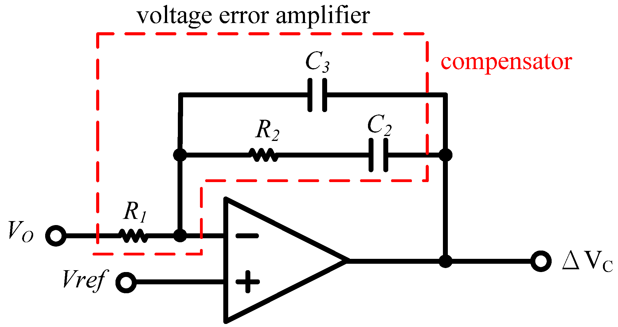
According to the previous specifications and the compensator of the proposed converter, parameter values of the small signal model in the proposed system (as shown in
Figure 16) are listed in
Table 1.
Table 1.
Parameter values of small signal model of the proposed converter.
Table 1.
Parameter values of small signal model of the proposed converter.
| symbol | parameter value |
|---|
| VO | 400 |
| D | 0.36 |
| L1 | 28 μH |
| N | 15 |
| CO | 780 μF |
| RL | 266.66 Ω |
| R1 | 10 kΩ |
| R2 | 220 Ω |
| C2 | 2 μF |
| C3 | 6.8 nF |
| VM | 2.5 |
| Kf | 160 |
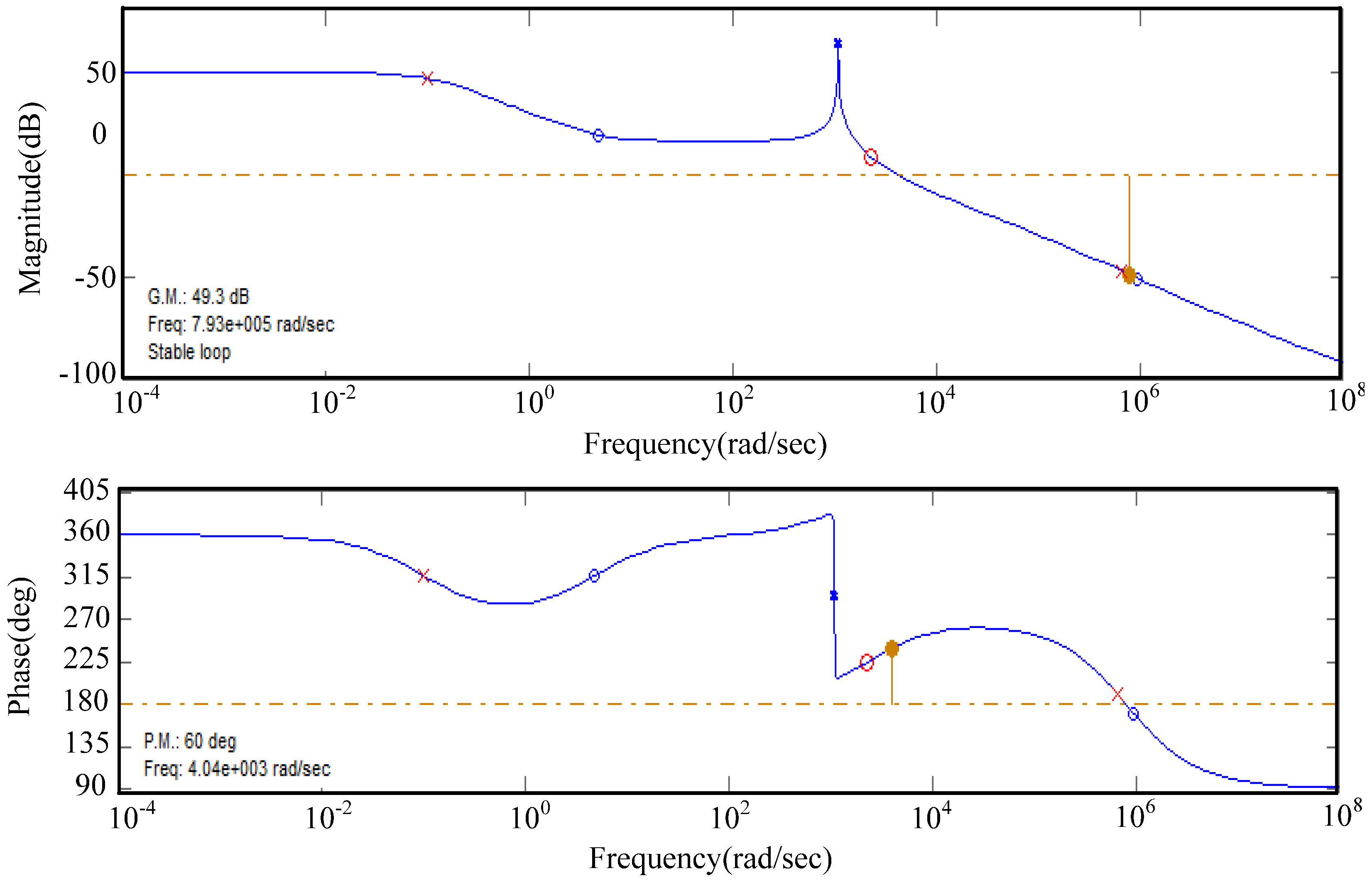
We can use the Matlab simulation tool to obtain Bode plots of the proposed converter under the closed loop condition. They are shown in
Figure 18. From
Figure 18, it can be seen that P.M. of the proposed one is 60°. Therefore, this can prove that the proposed converter is a stable system.
Figure 18.
Bode plots of the proposed converter under the closed loop condition.
Figure 18.
Bode plots of the proposed converter under the closed loop condition.
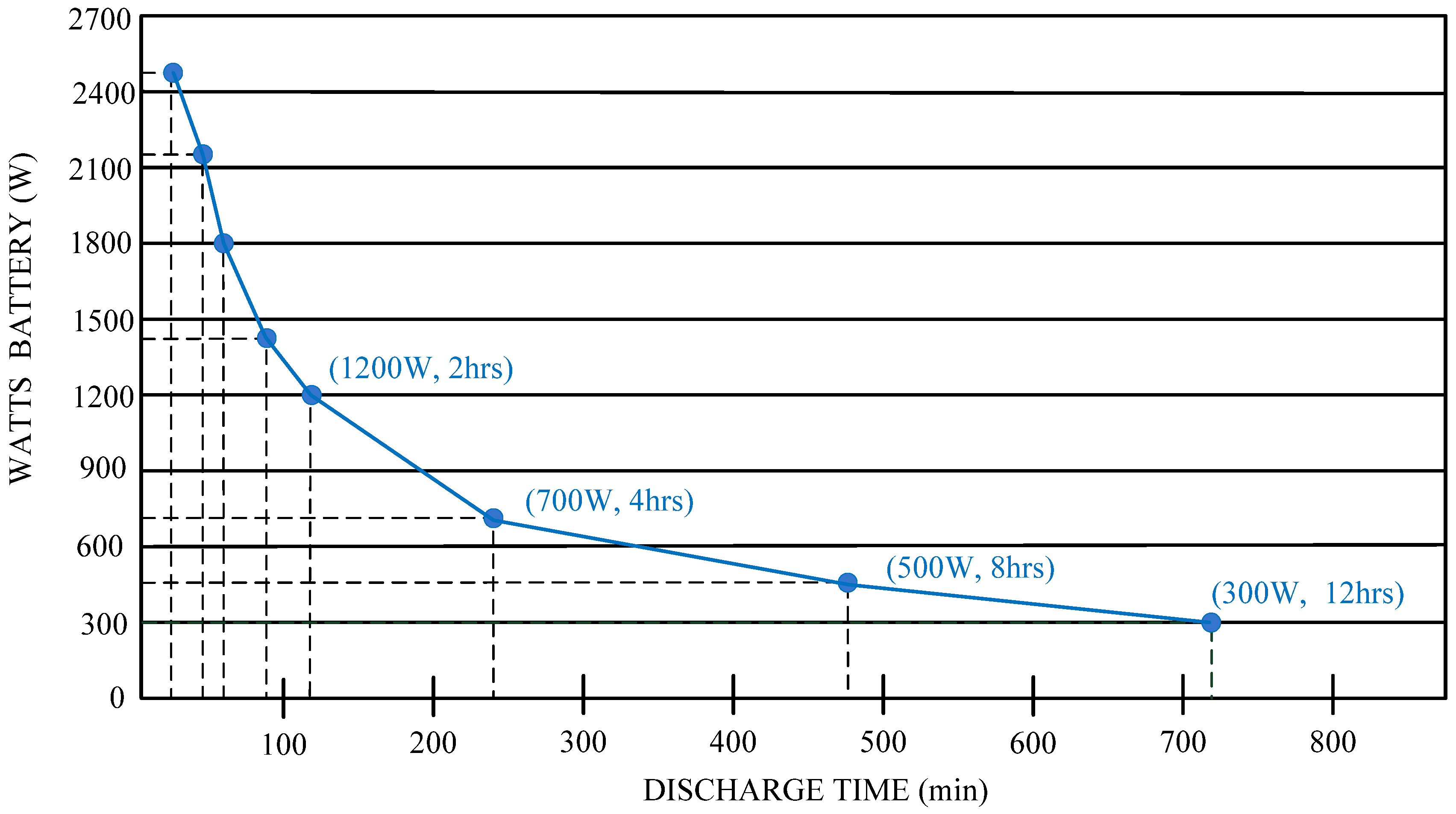
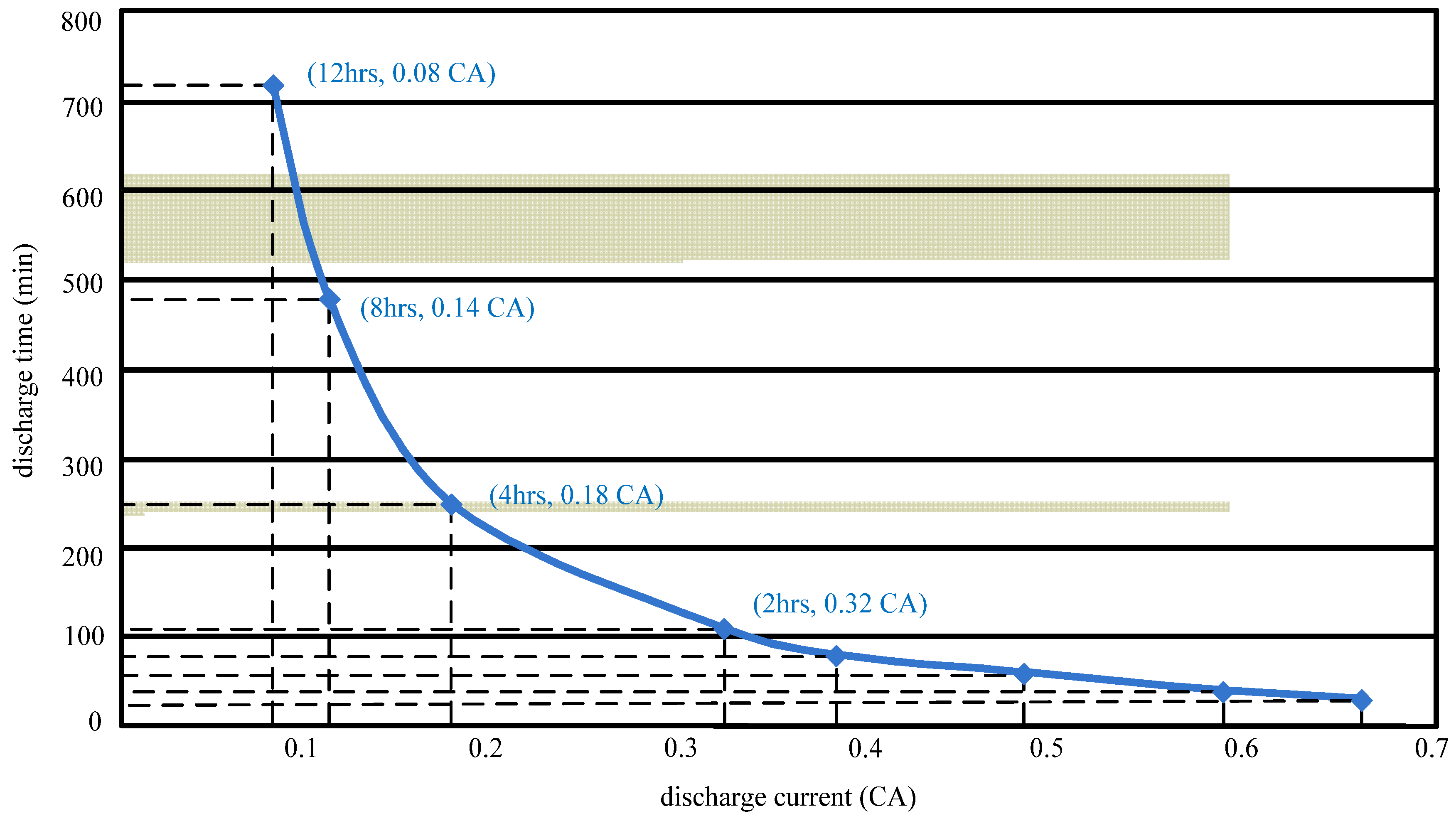
Since the proposed interleaved PV power system uses PV arrays and batteries as its input sources, the maximum output power of the proposed PV power system can supply 2.4 kW. In order to extend battery discharge time, the maximum output power of the battery module is suggested to be 1.2 kW. In our research, four sets of lead-acid batteries (12 V/75 Ah) connected in series are adopted in the proposed converter. According to discharge times supplied by the battery manufacturer, a sustained discharge time of 2 hours is possible when the output power of battery is 1.2 kW, while the discharge time can extend to 8 hours when it is 500 W. The curve of output power
versus discharge time of batteries as supplied by the battery manufacturer is shown in
Figure 19, while the curve of discharge time
versus discharge current (CA) of the batteries is depicted in
Figure 20.
Figure 19.
Plot of output power versus discharge time of the batteries supplied by battery manufacturer.
Figure 19.
Plot of output power versus discharge time of the batteries supplied by battery manufacturer.
Figure 20.
Plot of discharge time versus discharge current (CA) of batteries supplied by the battery manufacturer.
Figure 20.
Plot of discharge time versus discharge current (CA) of batteries supplied by the battery manufacturer.
From
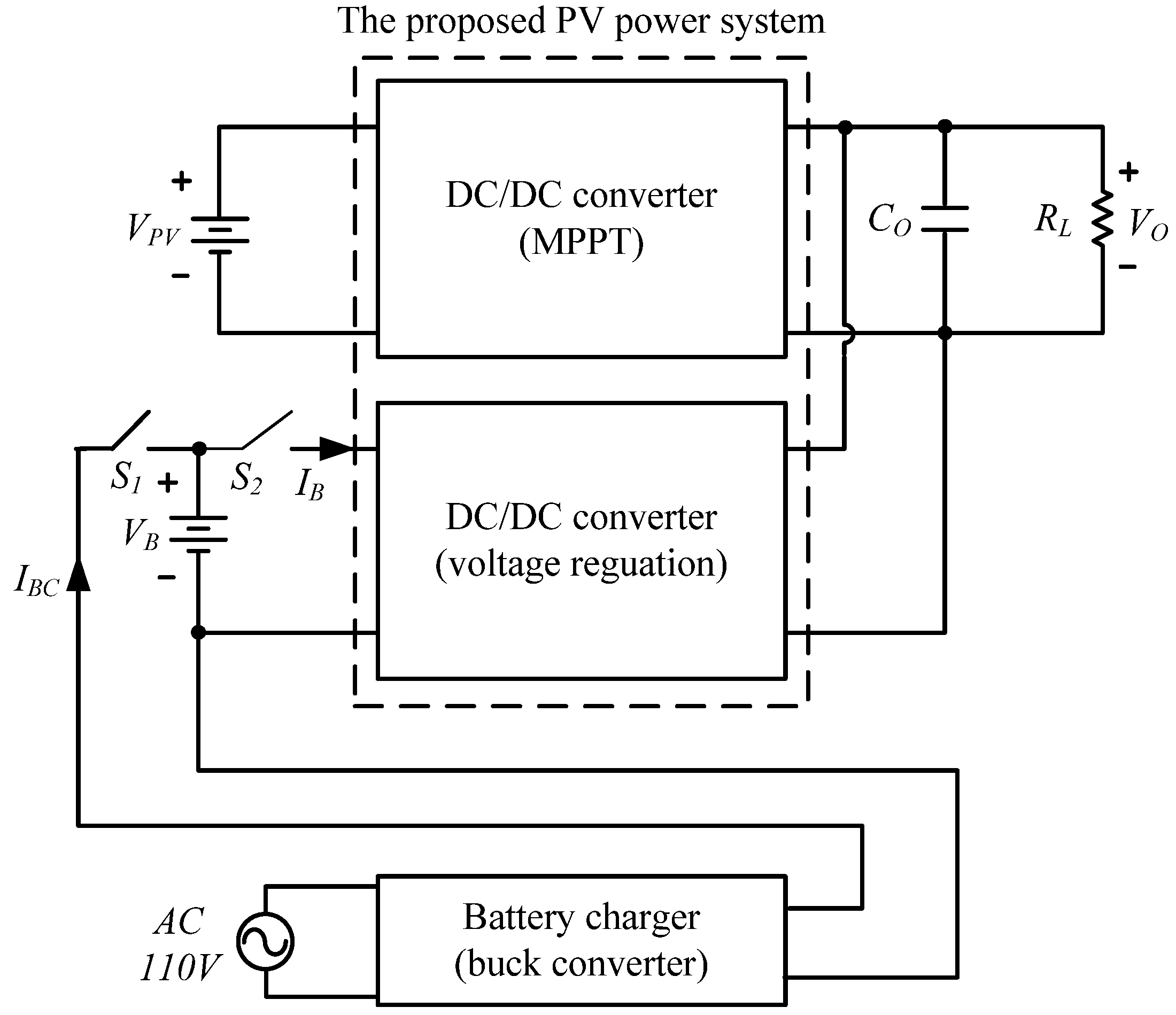
Figure 20, it can be seen that when output power of battery is 1.2 kW, its discharge current is 0.32 CA. When the battery is completely discharged, a battery charger is adopted. The block diagram of the proposed PV power system and battery charger is shown in
Figure 21. When the battery is in the charging state during the night, switch
S1 is turned on and a battery charger using a buck converter is adopted to charge the battery. On the other hand, when the battery in the discharging state during the day, switch
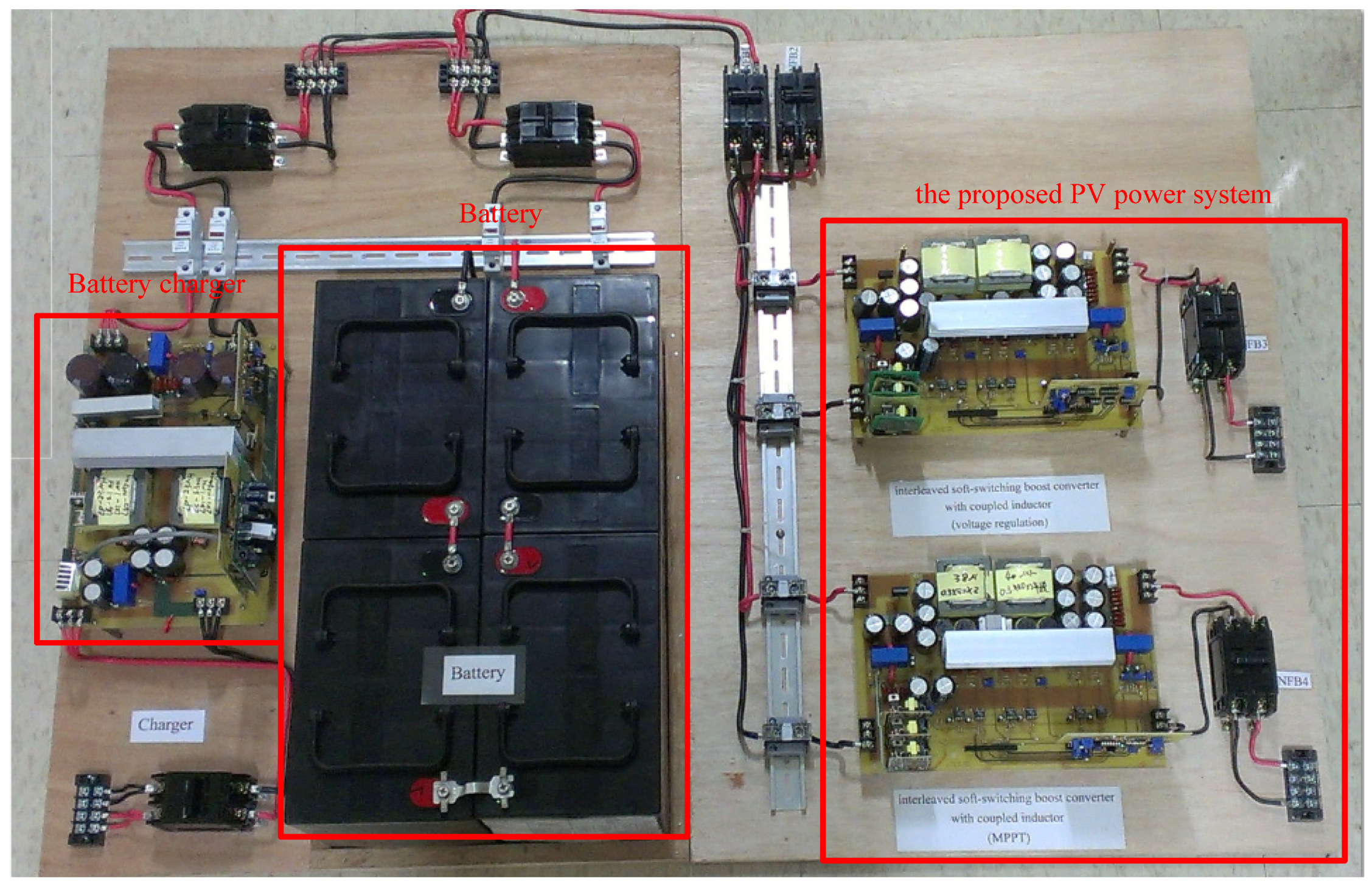
S2 is turned on and battery uses the proposed converter to supply power to the load. A photograph of the hardware is shown in
Figure 22.
Figure 21.
Block diagram of the proposed PV power system and battery charger.
Figure 21.
Block diagram of the proposed PV power system and battery charger.
Figure 22.
Photograph of the hardware for the proposed PV power system and battery charger.
Figure 22.
Photograph of the hardware for the proposed PV power system and battery charger.
Figure 23 shows measured charging voltage
VB and current
IBC waveforms of the battery, illustrating that the charging current
IBC uses the pulse current charging method and its charging current
IBC is under the repeat period of 200 ms, duty ratio of 0.5 and peak charging current of 20 A. When the battery voltage
VB reaches its end of charge voltage
VFV (about 54 V), the battery charger is shut down.
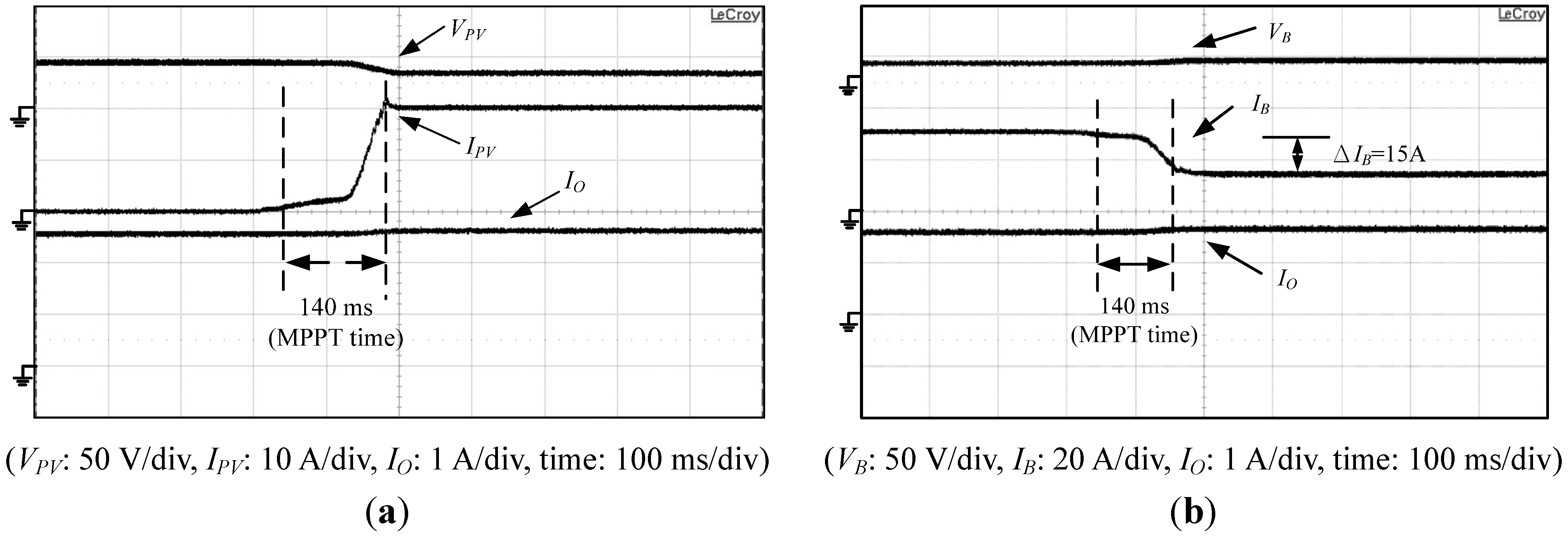
Figure 24 shows measured voltages and currents waveforms of the proposed PV power system under output power
PO of 1 kW and PV arrays maximum output power
PPV(max) of 700W.
Figure 24a shows measured PV arrays voltage
VPV, current
IPV and output current
IO waveforms, while
Figure 24b depicts measured battery voltage
VB, current
IB and output current
IO waveforms.
Figure 23.
Measured charge voltage VB and charge current IBC waveforms of battery under the repeat period of 200 ms, duty ratio of 0.5 and peak charging current of 20 A.
Figure 23.
Measured charge voltage VB and charge current IBC waveforms of battery under the repeat period of 200 ms, duty ratio of 0.5 and peak charging current of 20 A.
(VB: 20 V/div, IBC: 20 A/div, time: 100 ms/div)
Figure 24.
Measured voltage and currents waveforms of the proposed PV power system under output power PO of 1 kW and PV arrays maximum power PPV(max) of 700 W: (a) PV arrays voltage VPV, current IPV and output current IO waveforms; and (b) battery voltage VB, current IB and output current IO waveforms.
From
Figure 24, it can be seen that MPPT time of PV arrays is about 140 ms from 0 to 700 W and battery discharging current
IB varies from 30 A to 15 A. This proves that the proposed PV power system can regulate the output powers of the battery and PV arrays to supply power to the load.
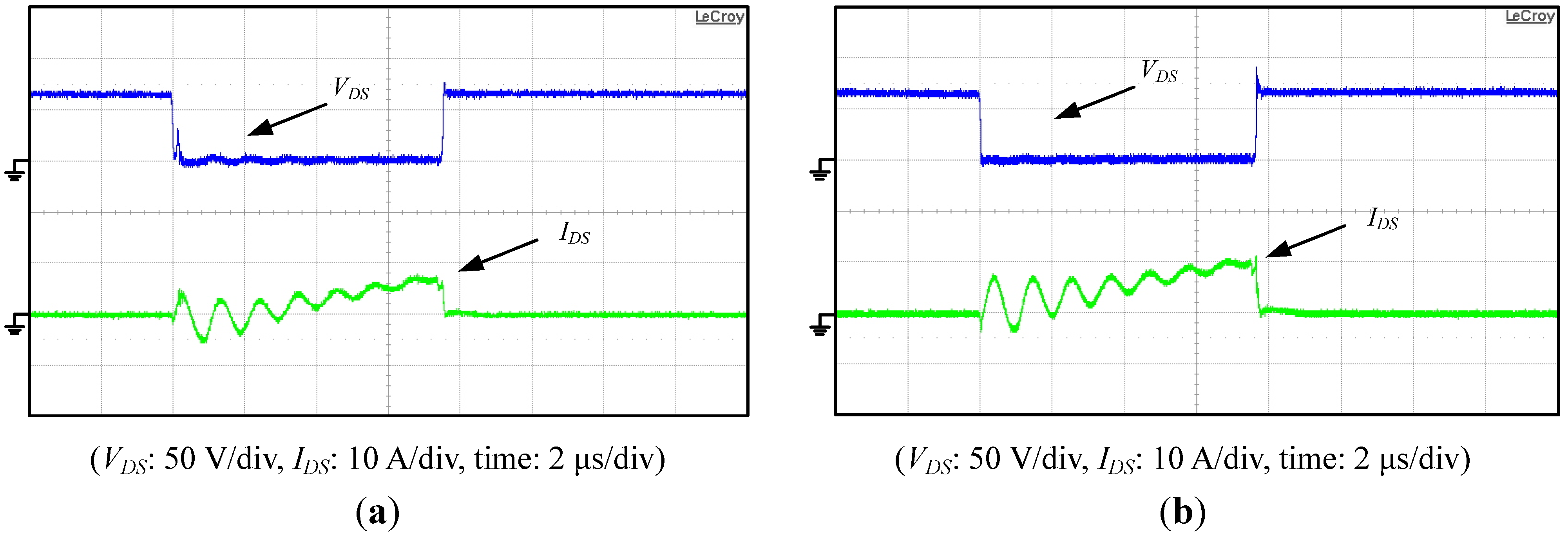
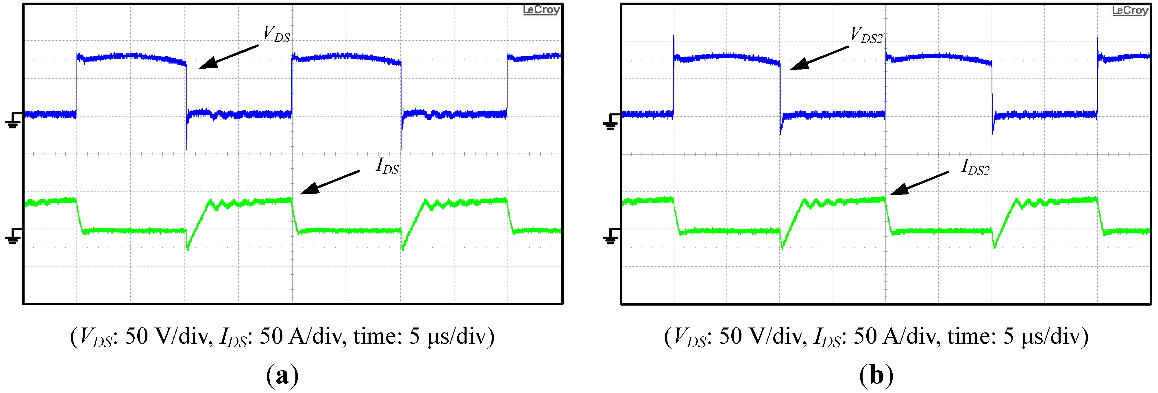
In order to verify the feasibility of the proposed interleaved active clamp boost converter with voltage regulation, measured voltage
VDS and
IDS waveforms of switches
M1B and
M2B are shown in
Figure 25 and
Figure 26, respectively.
Figure 27 shows those waveforms under 10% of full load condition, while
Figure 26 depicts those waveforms under full load condition. From
Figure 25, it can be found that when load is at 10% of full load condition, switches
M1B and
M2B are in the hard switching and soft switching boundary, respectively.
Figure 25.
Measured voltage VDS and current IDS waveforms of (a) switch M1B and (b) switch M2B of the proposed converter 10% of full load.
Figure 25.
Measured voltage VDS and current IDS waveforms of (a) switch M1B and (b) switch M2B of the proposed converter 10% of full load.
Figure 26.
Measured voltage VDS and current IDS waveforms of (a) switch M1B and (b) switch M2B of the proposed converter under full load.
Figure 26.
Measured voltage VDS and current IDS waveforms of (a) switch M1B and (b) switch M2B of the proposed converter under full load.
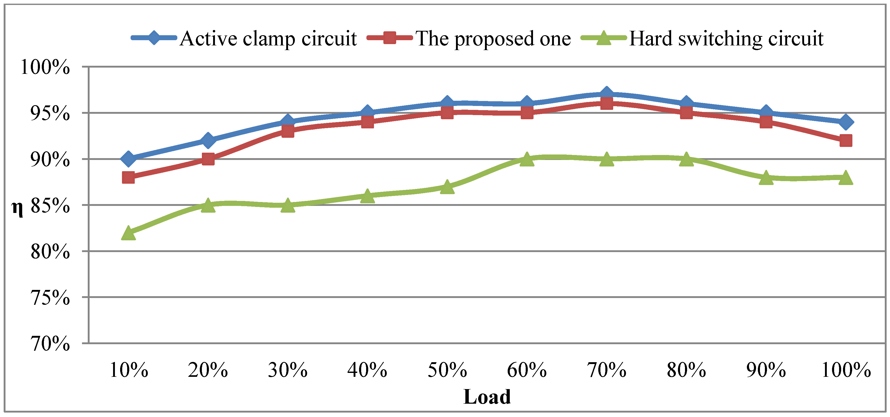
Figure 27.
Comparison conversion efficiency among the interleaved active clamp boost converter with hard-switching circuit, active clamp circuit and the proposed one.
Figure 27.
Comparison conversion efficiency among the interleaved active clamp boost converter with hard-switching circuit, active clamp circuit and the proposed one.
When the load is greater than 10% of full load, switches
M1B and
M2B can be operated with ZVS at turn on. Comparison of the conversion efficiency among the interleaved boost converter with hard-switching circuit, the active clamp circuit (as shown in
Figure 3) and the proposed one is shown in
Figure 27. It reveals that the efficiencies of the boost converter with the active clamp circuit and the proposed one are always higher than that with a hard-switching circuit from light load to heavy load. Moreover, efficiency of the boost with the proposed circuit is approximately the same as that with the active clamp circuit (as shown in
Figure 3) from light load to heavy load. The reason for this is that although currents flowing through diodes
D4B and
D6B have larger losses, compared with the boost converter with the active clamp circuit shown in
Figure 3, the diode current
ID6B, which flows through diode
D6B shown in
Figure 13, is the sum of current
IM2B and resonant current
IC1B. Since current
IC1B is a resonant current, the negative resonant current
IC1B, which is shown in
Figure 12 during
t9~
t10 interval, does not flow through diode
D6B. Therefore, this can partially reduce the forward conduction losses of diode
D6B. Similarly, the forward conduction losses of diode
D4B can also be reduced. As mentioned above, the boost converter with the proposed circuit can also keep it at a high conversion efficiency from light load to heavy load. Its maximum efficiency is 96% under 70% of full load conditions and its full load efficiency is about 92%. According to the efficiency curve of the proposed interleaved boost converter shown
Figure 27 and the circuit structure, its performance can compare with the results in [
28] and [
29]. The performance comparison results are listed in
Table 2. Note that the special capacitor is required to possess a lower ESR and a higher CRR and the special PWM IC possesses a larger duty ratio, greater than 0.5.
Table 2.
Performance comparison of interleaved high step-up converters.
Table 2.
Performance comparison of interleaved high step-up converters.
| High step-up interleaved converter | Converter in [28] | Converter in [29] | The proposed converter |
|---|
| Voltage gain | | | |
| Voltage stress on switch | | | |
| Voltage stress on diodes | | | VO + NVPV |
| Quantities of switches | 2 | 2 | 2 |
| Quantities of diodes | 6 | 4 | 4 |
| Quantities of cores | 4 | 2 | 4 (
) |
| Quantities of capacitors | 4 (special capacitors) | (special capacitors) | 3 |
| Maximum duty ratio | >0.5 | >0.5 | <0.5 |
| Controller | Complex (special PWM IC) | Complex (DSP) | Simple |
| Cost | High | Middle | Low |
| Efficiency | Higher | Higher | High |
| Power level | Small power | Small or middle power | Middle or high power |
In order to simply analyze the CRR
S of the proposed one and the conventional one proposed in [
29], we assume that values of output capacitors
C1, C2 and
C3 of the conventional one are equal to that of output capacitor
CO, and their voltages
VC1, VC2 and
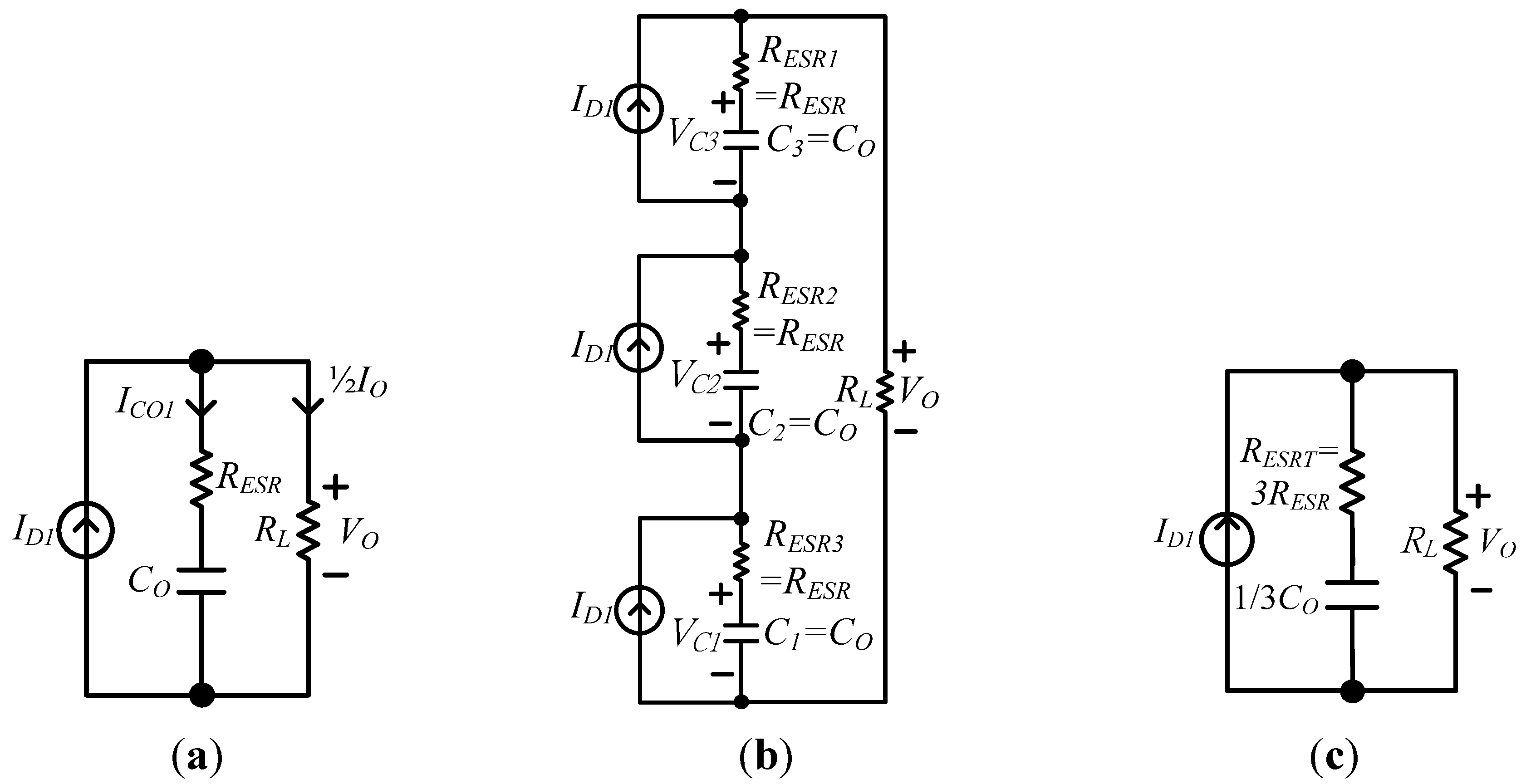
VC3 are the same value. Each output capacitor of the proposed one and the conventional one adopt the same current
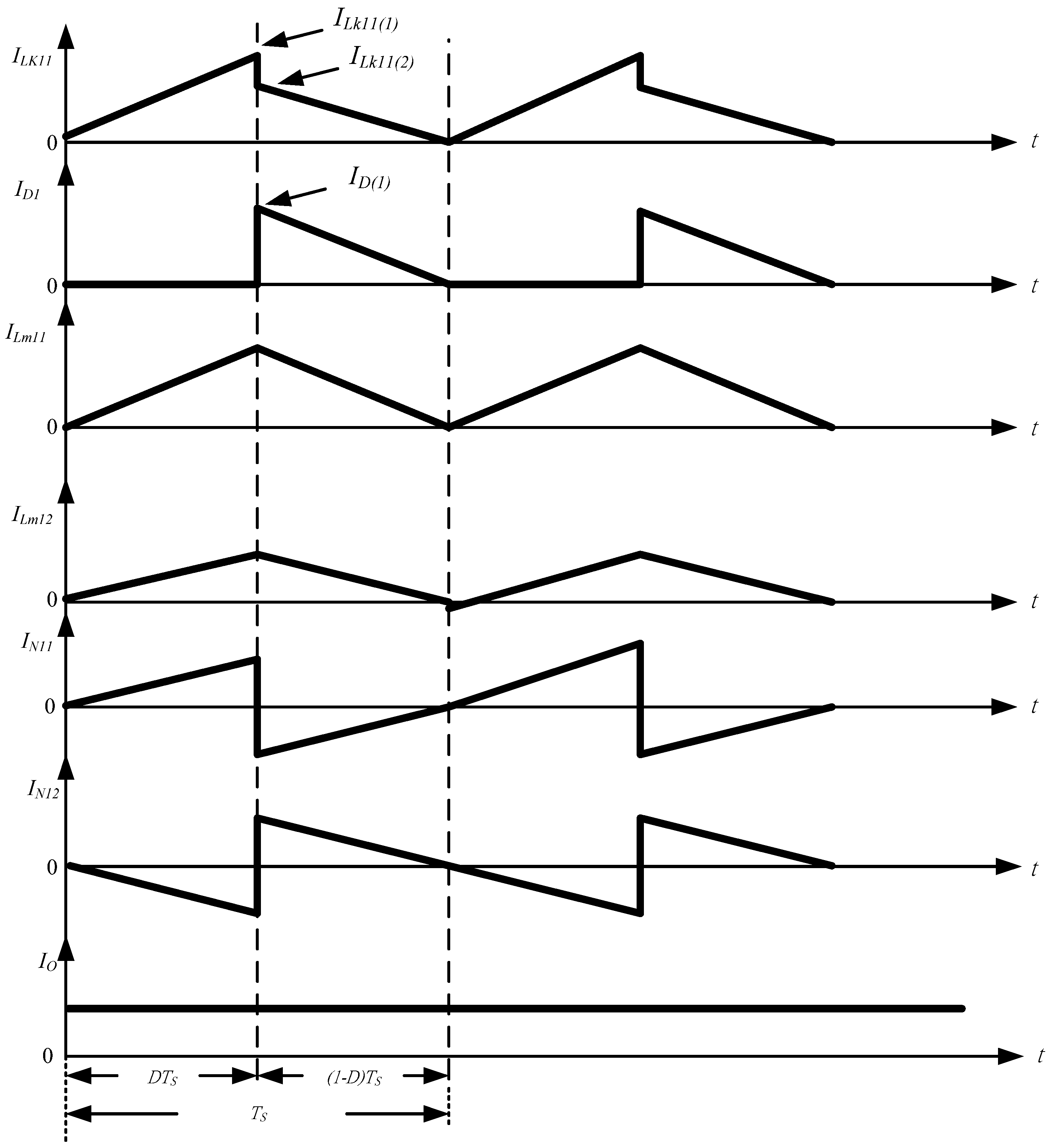
ID1 to charge them, as shown in
Figure 28. According to the previously assumed conditions, the equivalent circuit of the output terminals is shown in
Figure 29.
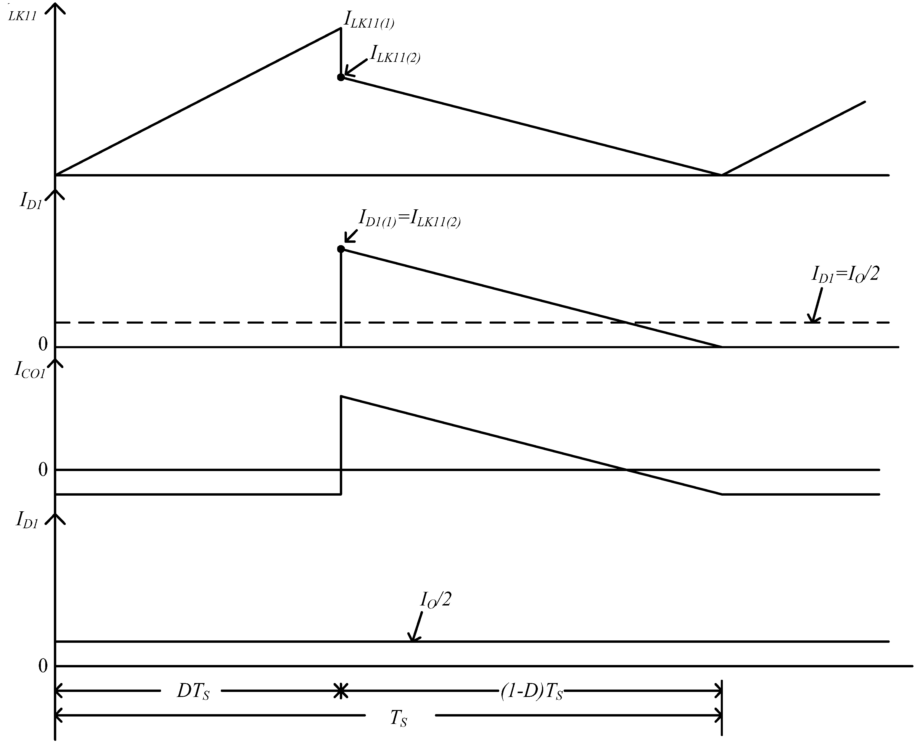
Figure 28.
Conceptual current waveforms of inductor current, diode current, output capacitor current and output current in the proposed converter operated converter operated in the boundary of CCM and DCM.
Figure 28.
Conceptual current waveforms of inductor current, diode current, output capacitor current and output current in the proposed converter operated converter operated in the boundary of CCM and DCM.
Figure 29.
Equivalent circuit of output terminals: (
a) the proposed converter; (
b) the conventional converter proposed in [
29]; and (
c) the simplified conventional converter proposed in [
29].
Figure 29.
Equivalent circuit of output terminals: (
a) the proposed converter; (
b) the conventional converter proposed in [
29]; and (
c) the simplified conventional converter proposed in [
29].
Figure 29a shows the one of the proposed converter, while
Figure 29b illustrates the one of the conventional one. Its simplified equivalent circuit is shown in
Figure 29c. From
Figure 29, it can be found that the equivalent ESR
RESRT (= 3
RESR) of the conventional one is greater than that of the proposed one. That is, output capacitors of the conventional one must have a higher CRR, which is proportional to the ESR of the capacitor. Therefore, the system reported in [
28] is suitable for low power level applications. The system in [
29] is applied to low or middle power level applications. The proposed PV power system can be applied to a middle or high power level application.
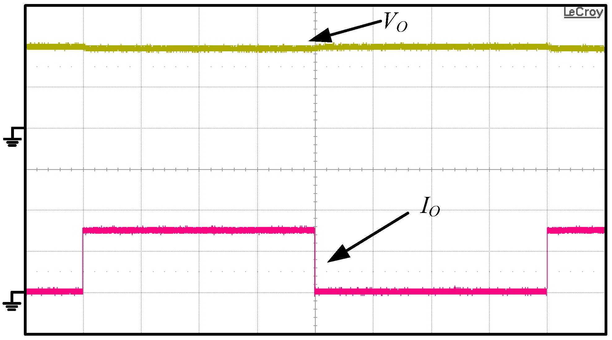
Figure 30 illustrates the step-load change be between 0% and 100% of full load, from which it can be observed that voltage regulation of output voltage
VO has been limited with in ±1% to prove a good dynamic response.
Figure 30.
Output voltage VO and output current IO under step-load changes between 0% and 100% of the full load condition of the active clamp interleaved boost converter.
Figure 30.
Output voltage VO and output current IO under step-load changes between 0% and 100% of the full load condition of the active clamp interleaved boost converter.
(VO: 200 V/div, IO: 2 A/div, time: 50 ms/div)
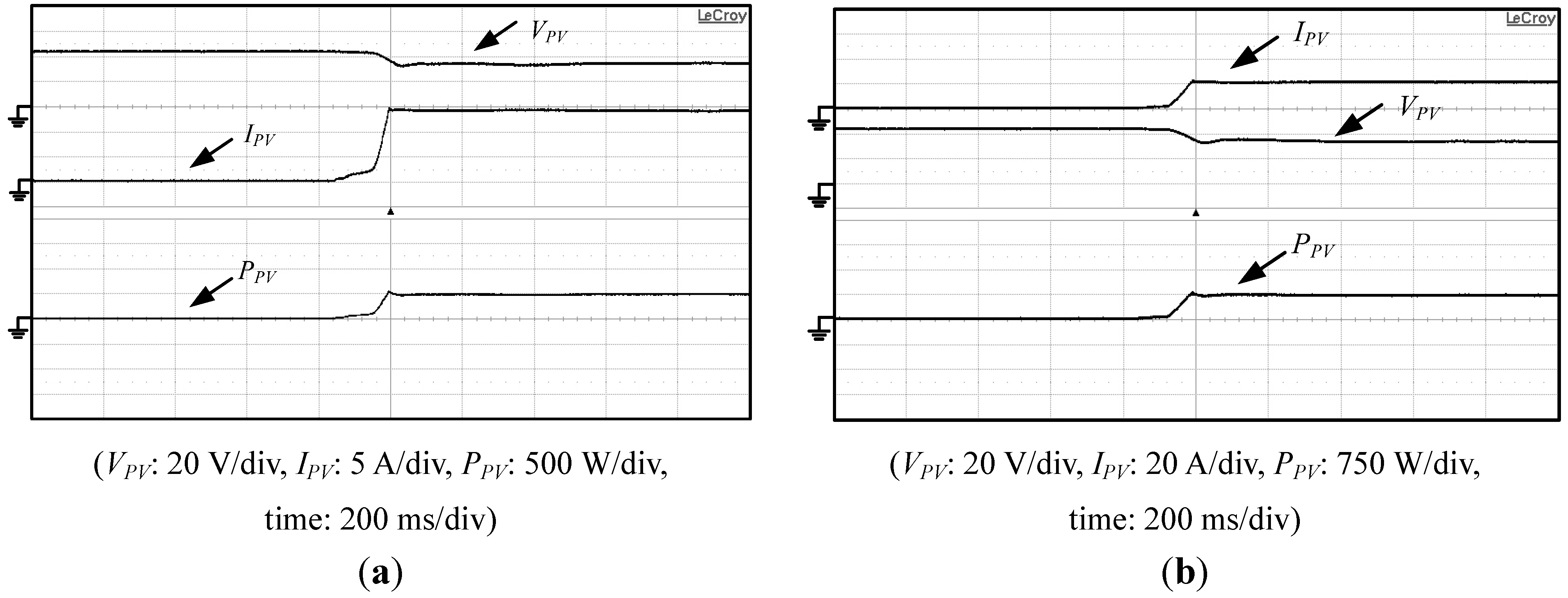
The MPPT waveforms of the proposed interleaved active clamp boost converter with MPPT are shown in
Figure 31.
Figure 31a shows those waveforms under the maximum PV arrays power of 500 W, while
Figure 31b illustrates those waveforms under the maximum power of 750 W. From
Figure 31, it can be found that the tracking time of MPPT is about 70 ms from 0 to the maximum power of PV arrays.
Figure 31.
Measured voltage VPV, current IPV and power PPV waveforms of PV arrays (a) under PPV(max) = 500 W; and (b) under PPV(max) = 750 W.
Figure 31.
Measured voltage VPV, current IPV and power PPV waveforms of PV arrays (a) under PPV(max) = 500 W; and (b) under PPV(max) = 750 W.
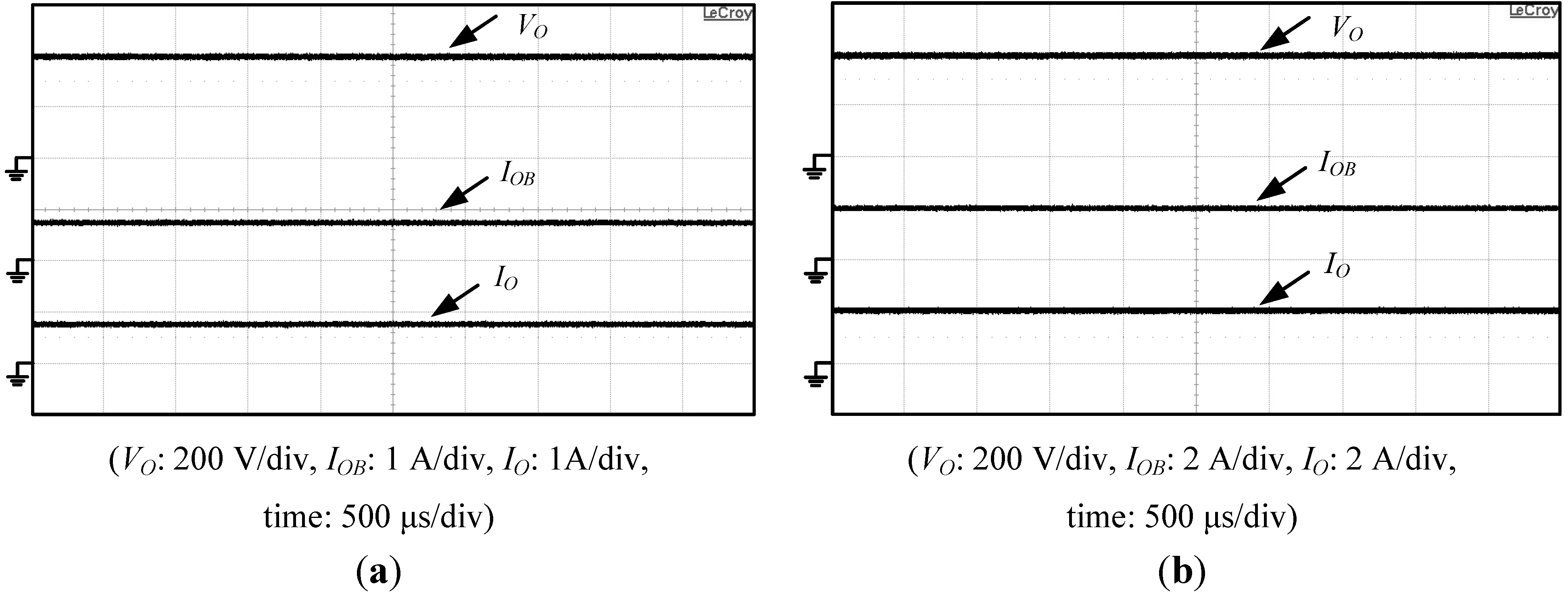
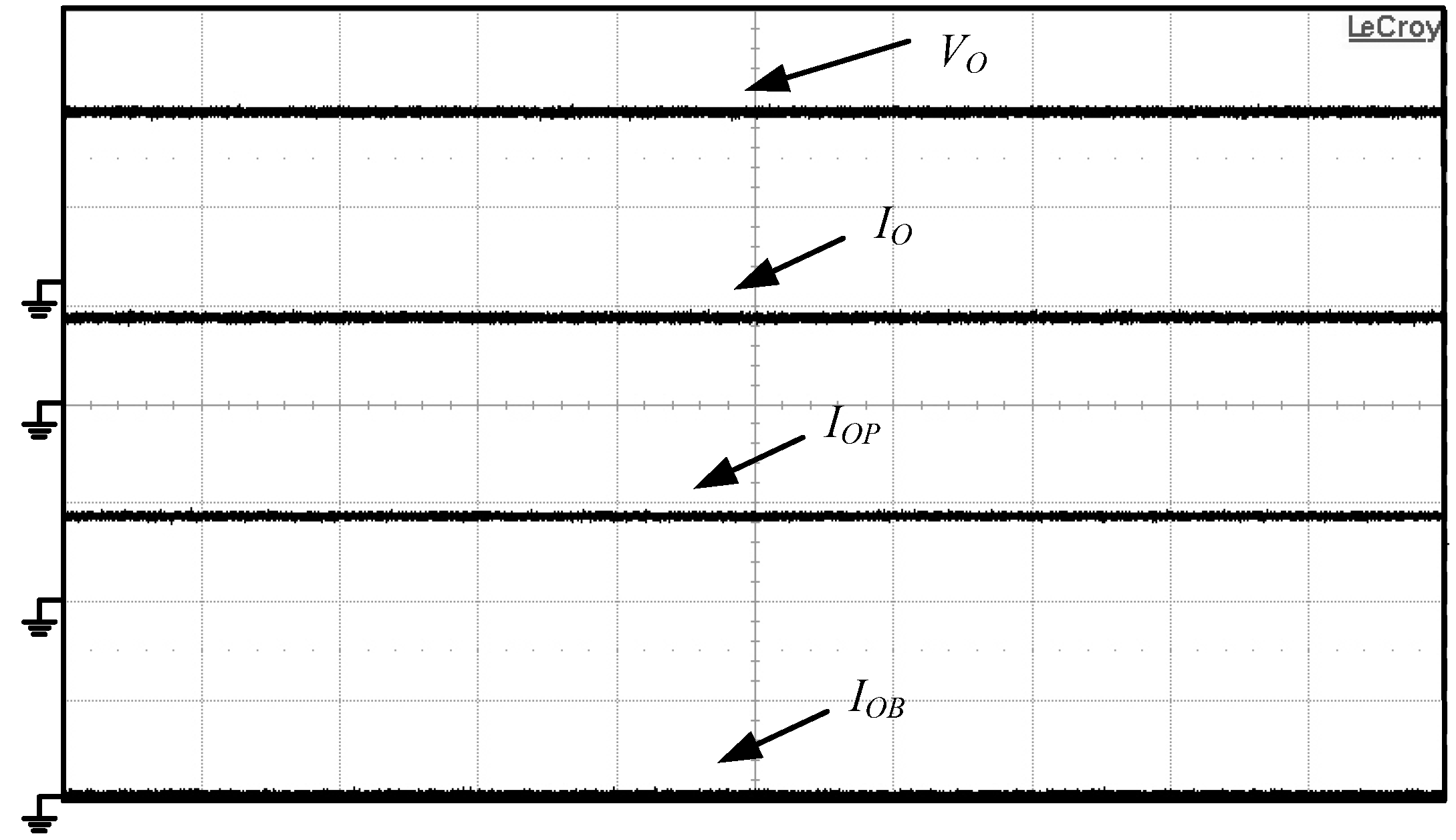
Measured output voltage
VO and current
IOB and
IO when the operational mode is within mode IV and
PVB(max) ≥
PL in power management of the proposed PV system is shown in
Figure 32.
Figure 32a depicts those waveforms under
PL = 320 W, while
Figure 32b shows those waveforms under
PL = 800 W. From
Figure 32, it can be seen that output voltage
VO is sustained at 400 V and current
IOB is equal to
IL.
Figure 32.
Measured voltage VO, current IOB and IO waveforms of the proposed PV power system operated in mode IV (a) under PL = 320 W; and (b) under PL = 800 W.
Figure 32.
Measured voltage VO, current IOB and IO waveforms of the proposed PV power system operated in mode IV (a) under PL = 320 W; and (b) under PL = 800 W.
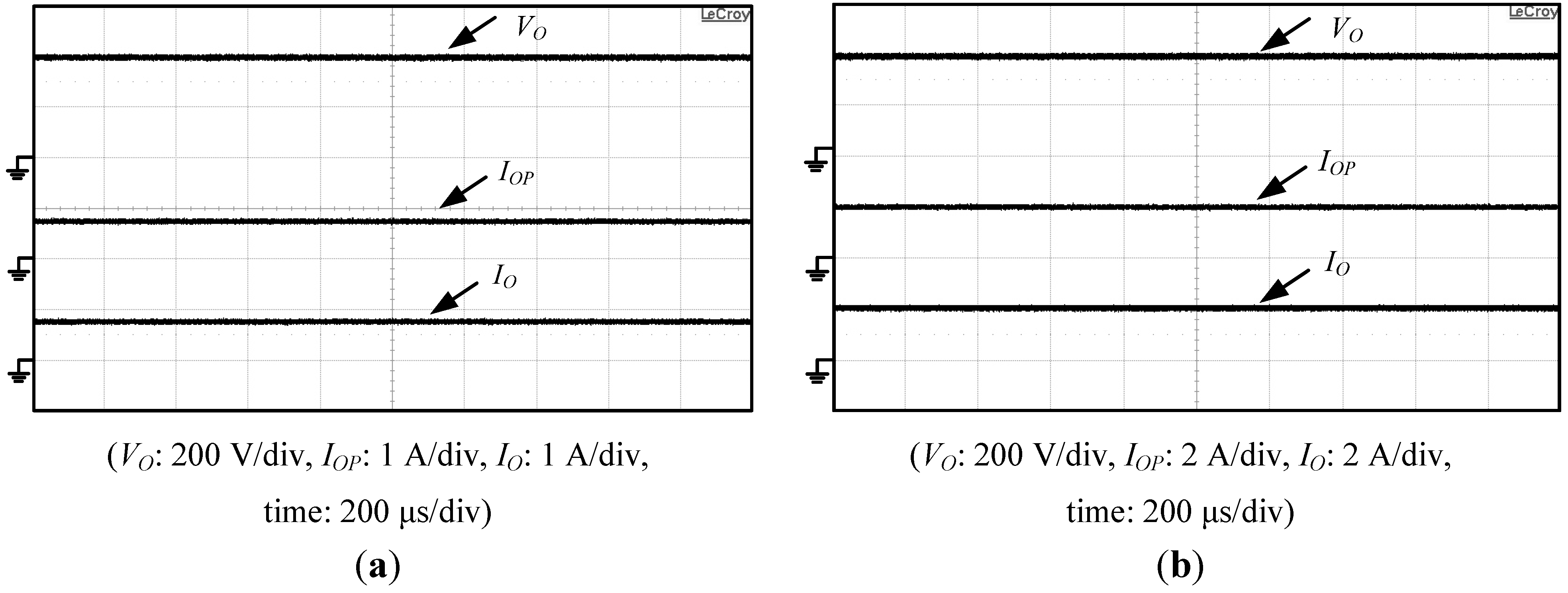
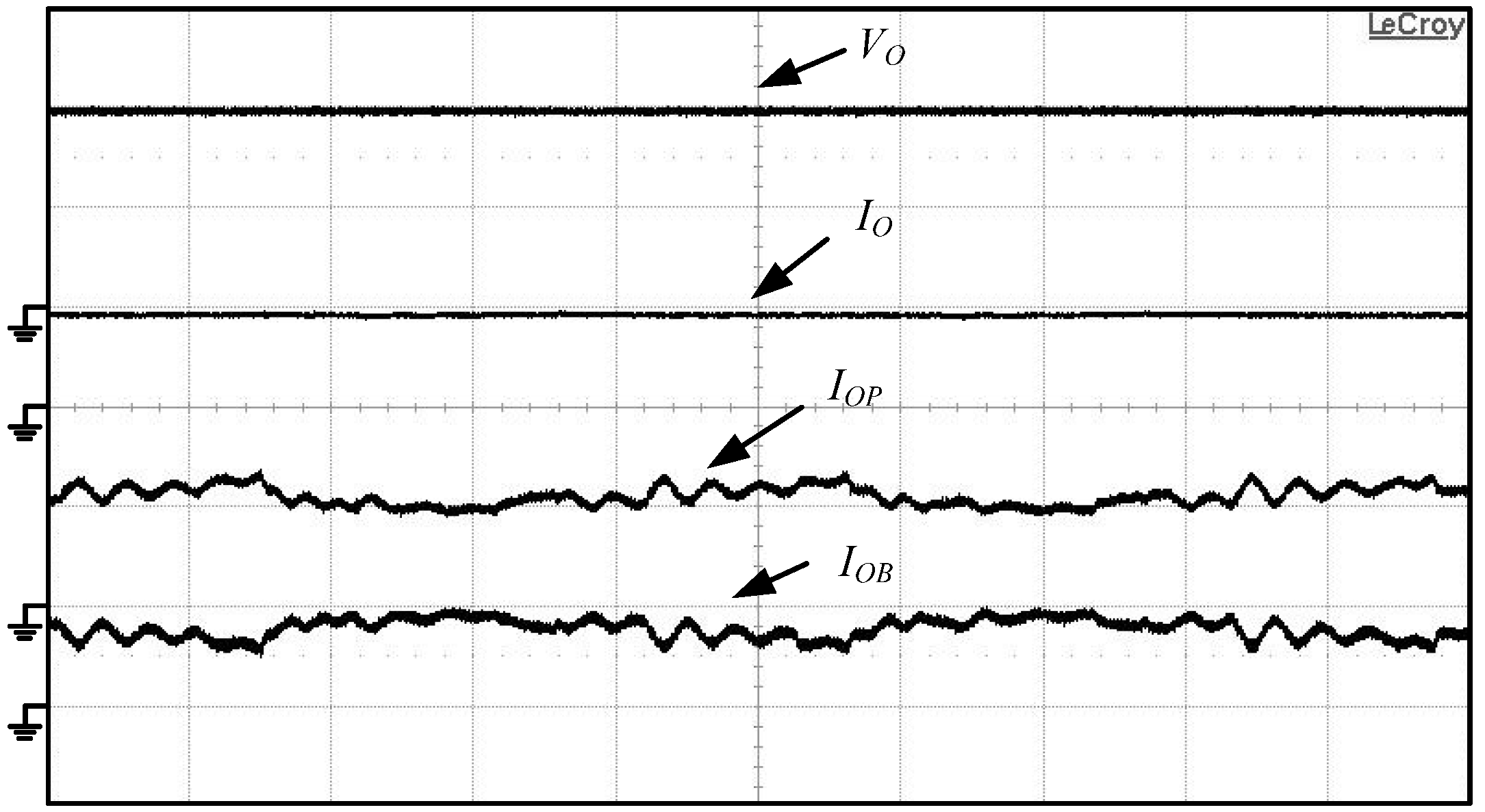
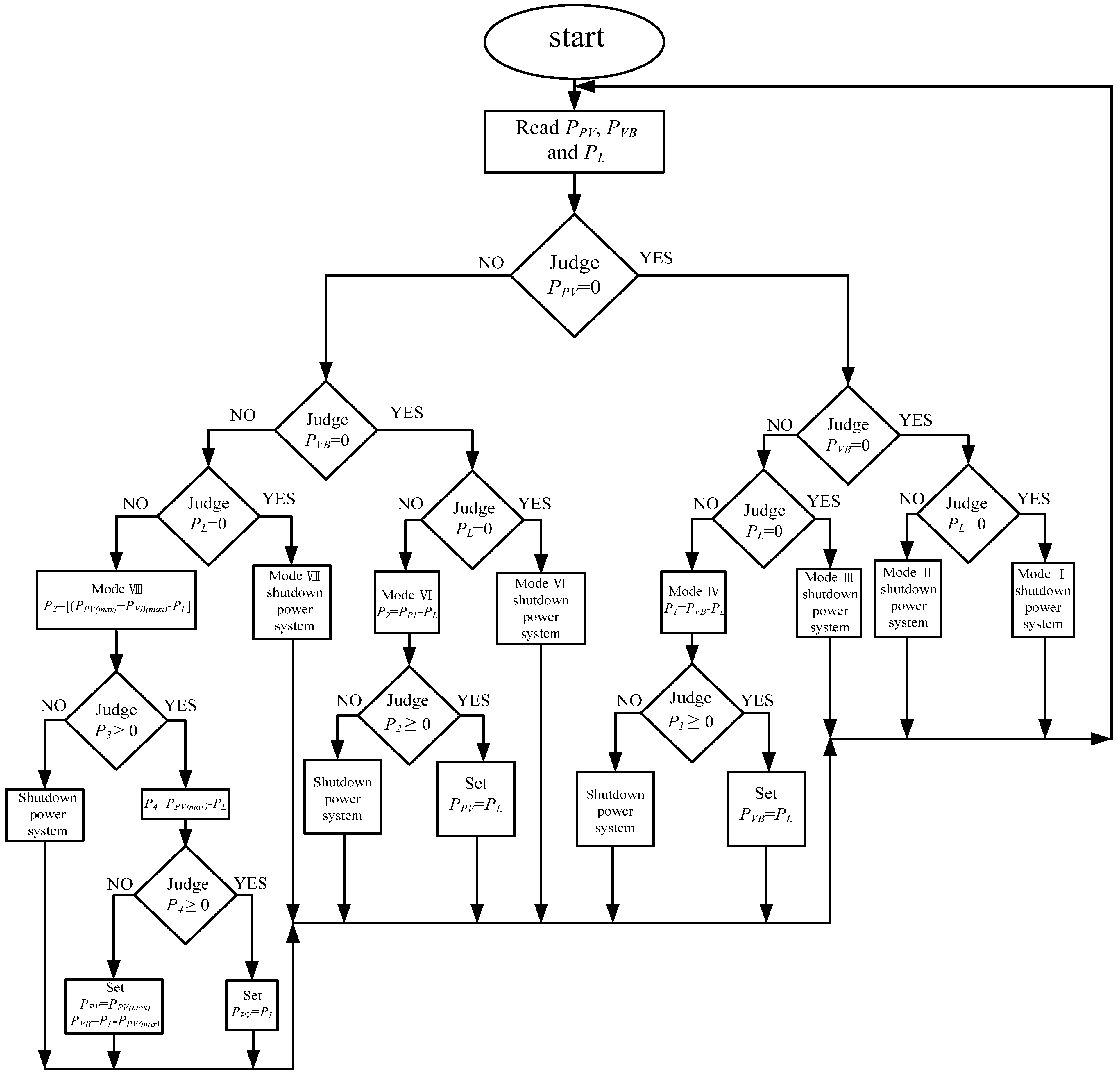
When the operational mode of the proposed PV power system is mode VI and
PPV(max) ≥
PL, its measured output voltage
VO and current
IOP and
IL waveforms under
PPV(max) = 800 W and
PL = 320 W are shown in
Figure 33a, illustrating that output voltage
VO is clamped at 400 V, current
IOP is equal to
IL and
PPV = 320 W.
Figure 33b shows those waveforms under
PL = 800 W. When
PL = 800 W, output power
PPV is also equal to 800 W and it is operated at its MPP. As mentioned above, operational modes of the proposed PV power system are respectively in the mode IV and VI states, the proposed one can regulate power between PV arrays, battery and load.
Figure 33.
Measured voltage VO, current IOP and IO waveforms of the proposed PV power system operated in mode VI (a) under PL = 320 W; and (b) under PL = 800 W.
Figure 33.
Measured voltage VO, current IOP and IO waveforms of the proposed PV power system operated in mode VI (a) under PL = 320 W; and (b) under PL = 800 W.
When the operational mode of the proposed one is mode VIII and (
PPV(max) +
PVB(max)) ≥
PL, its operational conditions are divided into two conditions. One is
PPV(max) ≥
PL and the other is
PPV(max) <
PL. When
PPV(max) ≥
PL, its measured output voltage
VO, and currents
IOP,
IOB and
IL waveforms under
PPV(max) = 750 W and
PL = 375 W are shown in
Figure 34. Under this operational condition, current
IOP is equal to
IO and
IOB is equal to 0. That is, the proposed boost converter with MPPT is used to supply power to the load and the PV arrays are not operated at MPP, while the proposed boost one with voltage regulation is shut down. When
PPV(max) <
PL, its measured output voltage
VO, and currents
IOP,
IOB and
IO under
PPV(max) = 375 W and
PL = 750 W is shown in
Figure 35, illustrating that output voltage
VO is still lamped at 400 V and
IO =
IOP +
IOB. That is, the PV arrays can be operated at the maximum power point of 375 W and the battery can supply power to the load for balancing the power between the PV arrays and load. From experimental results, it can be seen that the proposed PV power system can use its power management circuit to achieve power balance between PV arrays, batteries and loads.
Figure 34.
Measured voltage VO, current IOB, IOP and IO waveforms of the proposed PV power system operated in mode VIII under (PP(max) + PVB(max)) ≥ PL and PPV(max) ≥ PL.
Figure 34.
Measured voltage VO, current IOB, IOP and IO waveforms of the proposed PV power system operated in mode VIII under (PP(max) + PVB(max)) ≥ PL and PPV(max) ≥ PL.
(VO: 200 V/div, IO: 1 A/div, IOP: 1 A/div, IOB: 1 A/div, time: 200 μs/div)
Figure 35.
Measured voltage VO, current IOB, IOP and IO waveforms of the proposed PV power system operated in mode VIII under (PP(max) + PVB(max)) ≥ PL and PPV(max) < PL.
Figure 35.
Measured voltage VO, current IOB, IOP and IO waveforms of the proposed PV power system operated in mode VIII under (PP(max) + PVB(max)) ≥ PL and PPV(max) < PL.
(VO: 200 V/div, IO: 1 A/div, IOP: 1 A/div, IOB: 2 A/div, time: 200 μs/div)






 ,
,  (IL1, IL2 and D are the steady components, while
  and
and  are the small disturbance quantities ), and iL2 = (1 − d)iL1 in Equations (2) and (3), they can be rewritten by Laplace transformation and be expressed by:


