1. Introduction
Since fossil fuels will be depleted in the next decades, development of green energy power generation systems becomes urgent. Among renewable energy generation systems, photovoltaic (PV), wind turbine, energy storage systems, and fuel cells attract a lot of attention [
1,
2,
3,
4]. Nevertheless, low output voltage is their common shortcoming, especially in grid connection or electric vehicle (EV) applications. Therefore, a step-up converter to achieve high voltage gain is required. Conventional boost-type converters, like boost, buck-boost, and flyback, are able to step-up input voltage. However, in order to meet high-voltage gain requirements, they have to operate in heavy-duty ratio or adopt a high turns ratio transformer, which will decrease the conversion efficiency dramatically. Cascading more boost-type converters can avoid the above problem but issues of volume, cost, and efficiency emerge. Therefore, the high step-up DC/DC converter is the current design trend.
High step-up converters can be mainly classified into two categories: single-stage and interleaved structure. Single-stage topology incorporates coupled inductors and/or switched capacitors to complete high voltage gain. Even though its input voltage is boosted, a large magnitude of input current ripple occurs, limiting the converter power rating significantly [
5,
6,
7,
8]. The interleaved converter has the ability of suppressing input current ripple by means of adding a parallel current path, which is a better choice for high power applications [
9,
10,
11]. However, the conventional interleaved converters have voltage gain limitation, which confines their applications in grid-tied systems. To overcome the aforementioned disadvantages, various high step-up interleaved converters were proposed in [
12,
13,
14,
15,
16]; nevertheless, the shortcomings of lower voltage gain, higher voltage stress, and large component count still exist. An interleaved Boost converter combining voltage doubler is introduced in [
12], while a coupled inductor is examined in [
13]. In order to achieve high voltage gain, the converters in [
12,
13] have to be operated at heavy-duty ratio or adopt a magnetic transform with high turns ratio, which results in low conversion efficiency or high voltage stress. Even though Lai et al. [
14] proposed another high step-up converter, incorporating coupled inductor and switched capacitor, into an interleaved Boost configuration, the converter intrinsically has the demerits of higher voltage stress and sophisticated structure. An interleaved step-up converter with winding-cross-coupled inductors and voltage multiplier cells is presented in [
15]. This converter is composed of eight semiconductor devices and two three-winding coupled inductors. That is, a large number of power devices must be used. Tseng et al. [
16] utilized the characteristics of forward, flyback, and interleaved converters to boost input voltage, but voltage gain still is limited.
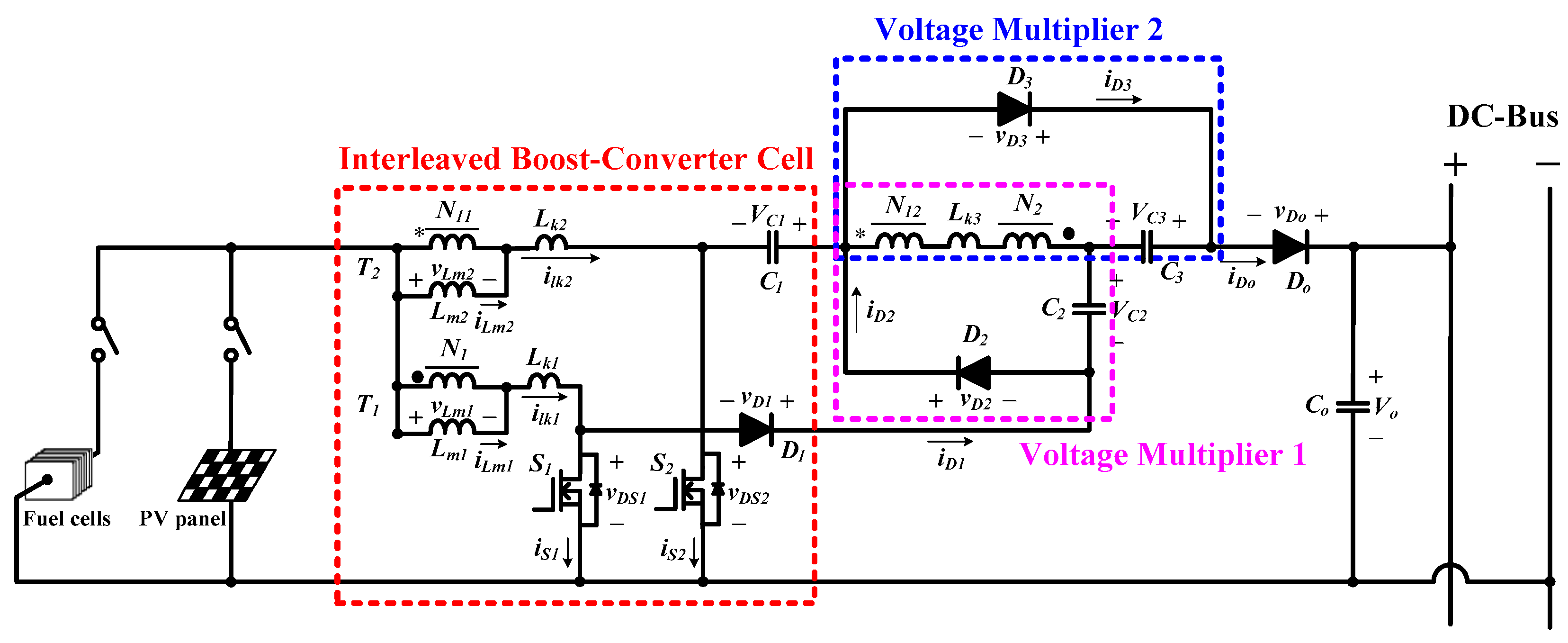
This paper proposes a novel interleaved converter (NIC), which can accomplish a high voltage conversion ratio and is capable of processing low voltage, high power distributed resources. Its power stage is depicted in
Figure 1. The proposed NIC mainly includes three parts: one interleaved-boost converter cell and two voltage multipliers. The interleaved-Boost converter cell is in charge of lowering input current ripple, increasing current rating, and primarily stepping input voltage. The two voltage multipliers can further stack up voltage level. The series voltage of the three parts determines the magnitude of output voltage. Since the proposed converter only uses two coupled inductors, three capacitors, four diodes, and two active power switches, it has a lower component count and a simple circuit structure. The advantages of the proposed NIC are summarized as follows:
- (1)
The NIC can suppress input current ripple.
- (2)
The energy stored in leakage inductance can be recycled.
- (3)
The voltage stress of the semiconductor device is low enough so that a power switch with lower on-state resistance and smaller parasitic capacitance can be chosen.
- (4)
As compared with a conventional interleaved high step-up converter, the proposed NIC can achieve a much higher voltage gain under the same power component count.
2. Operation Principle of the Proposed Converter
In
Figure 1,
Lm1 and
Lm2 denote the magnetizing inductances of the coupled inductors
T1 and
T2, respectively. The
Lk1 and
Lk2 represent the primary leakage inductances of
T1 and
T2, in turn, while
Lk3 stands for the total leakage inductance at the secondary windings of both coupled inductors. Turns ratios of primary to secondary of
T1 and
T2 are denoted as
n1 and
n2, respectively.
C1,
C2, and
C3 are the main capacitors employed in the circuit. It is supposed that the NIC operates in continuous conduction mode (CCM) and the two active switches
S1 and
S2 are controlled in interleaved manner. Accordingly, the operation of the NIC can be divided into ten operation modes over one switching cycle. The corresponding equivalents are illustrated in
Figure 2, while
Figure 3 depicts key waveforms. Analysis of the proposed NIC begins by making these assumptions:
- (1)
All parasitic capacitances and internal resistances are neglected. Moreover, all diodes are ideal.
- (2)
The voltages across capacitors C1, C2, C3, and Co are time-invariant.
- (3)
Magnetizing inductances, Lm1 and Lm2, are much larger than the leakage inductances Llk1, Llk2 and Llk3.
- (4)
The switching period is Ts. Both switches are closed for time DTs and open for (1 − D)Ts.
Mode 1 (t0–t1) (Figure 2a): This mode is the initial mode of the all operation procedures. During this time interval, both active switches
S1 and
S2 are closed. Diodes
D1,
D3 and
Do are in reverse-bias, but
D2 is forward-biased. Input voltage
Vin is across the primaries of
T1 and
T2 directly. Then, the current flowing through
S2 starts increasing linearly from zero, while the switch current
iS1, having an initial value determined by the end of Mode 10, also increases linearly. In addition, the energy remained in
Lk3 will be recycled to
C2 via
D2. At the time that the diode current
iD2 drops to zero, and this mode ends.
Mode 2 (t1–t2) (Figure 2b): During this time interval, active switches
S1 and
S2 are still closed, and
Vin remains across the two coupled inductors
. Thus, the current
iLm1 and
iLm2 are continuously increasing. In this mode, the current flowing through leakage inductances
ilk1 and
ilk2 are equal to magnetizing-inductance currents
iLm1 and
iLm2, respectively. This mode ends when the switch
S1 is turned off.
Mode 3 (t2–t3) (Figure 2c): In this mode,
S2 remains in on state but
S1 becomes off. Diodes
D2,
D3 and
Do are reversely-biased but
D1 is in forward-bias. The
Vin,
Lm1,
Lk1 and
C2 dump energy to
Lk3 and
C1 via
D1 and
S2, so the current flowing through
D1 and
S2 increases. This mode finishes when
D3 becomes forward-biased and
Lk3 starts to release energy.
Mode 4 (t3–t4) (Figure 2d): Over the whole interval of Mode 4,
S2 is still kept in on state while
S1 in off state. The
D1 remains forward-biased and
D3 becomes closed. Meanwhile, both diodes
D2 and
Do continue the off status. Magnetizing-inductance
Lm1 pumps energy to
C3 via the coupled inductor. Capacitor
C1 is charged continuously, the circuit behavior of which is the same as in the previous mode. When the leakage-inductance
Lk1 releases over its stored energy,
iD1 will drop to zero. That is, diode
D1 becomes reversely-biased and this mode ends.
Mode 5 (t4–t5) (Figure 2e): During this time interval,
S2 is still closed and
S1 is open. Diodes
D1,
D2 and
Do are reversely-biased but
D3 is in forward-bias.
Vin and
Lm1 supply energy to
C3 simultaneously by the
T1 and
T2 in turn. This mode finishes as
S1 is turned on.
Mode 6 (t5–t6) (Figure 2f): During this mode,
S1 and
S2 are both in on state. Diodes
D1,
D2 and
Do are off, but
D3 is on.
Lm1 starts to draw energy from
Vin. The stored energy in
Lk3 will releases to
C3 through
D3. This mode sustains until
iD3 decreases to zero.
Mode 7 (t6–t7) (Figure 2g): During this time interval,
S1 and
S2 are both in on state, but
D1,
D2,
D3 and
Do are all reversely-biased. Since the primaries of the two coupled inductors are in parallel,
Vin will supply energy to
Lm1,
Lm2,
Lk1 and
Lk2. Therefore,
iLm1 and
iLm2 will increase linearly, which are identical to
iS1 and
iS2, respectively. This mode is ended when
S2 is turned off.
Mode 8 (t7–t8) (Figure 2h): During this time interval,
S1 remains in on state, but
S2 in off state.
D1,
D2 and
D3 are off, but
Do is on. The
Lm2 starts to release its stored energy so that the current flowing through
Lm2 decays. Meanwhile, the current
ilk3 increases. The input
Vin and the voltages across
Lm2,
Lk2,
C1, and
C3 will be stacked up to supply
Co. This mode terminates when
Lk3 starts to charge
C2.
Mode 9 (t8–t9) (Figure 2i): In this mode,
S1 is still closed and
S2 is open. The
Vin will charge
C2 via coupled inductor
T1; meanwhile, the energy stored in
Lm2 will also be transferred to the secondary of
T2 for powering
C2. Therefore,
iLm2 drops and
Co keeps on charging. In Mode 9, the energy in
Lk2 is recycled to the output. This mode ends as
ilk2 falls to zero.
Mode 10 (t9–t10) (Figure 2j): The diode
Do will become reversely biased when
ilk2 drops to zero. In Mode 10,
S1 proceeds with on-state conducting and
S2 remains in off state. With respect to diode status, the diodes
D1,
D3 and
Do are in reverse-bias and
D2 is still in on state. The
Vin and
Lm2 will forward energy to
C2 through the coupled inductors
T1 and
T2, respectively. This mode ends when
S2 is turned on again, and then the operation returns to Mode 1.
3. Voltage Gain Derivation
Voltage gain is the most important characteristic of a high step-up converter. As the analysis in
Section 2 shows, the switched capacitors
C1 and
C3 have the benefit of voltage stacking for achieving extra-high voltage gain. This section focuses on the voltage gain derivation of the proposed NIC. For high power applications, the converter is designed in CCM. Assumptions made in
Section 2 are also adopted for simplifying the derivation. Furthermore, the coupling coefficients of the coupled inductors are both supposed at unity; that is, there is no leakage inductance.
According to the description for Mode 4 in
Section 2,
C1 is charged by
Vin,
C2,
T1, and
T2, whereas
C3 is charged by the two coupled inductors. Referring to Mode 9 in
Section 2, if the leakage inductances are ignored, the output port is supplied by
Vin,
T1,
T2,
C1, and
C3. Hence, to determine the voltage gain,
Vo/
Vin, the relationships of
VC1,
VC2 and
VC3 in terms of
Vin have to be found in advance.
3.1. The Ratio of VC3 to Vin
As S1 is closed, Vin will supply energy to Lm1. After an on-time interval DTs, the change in iLm1 can be estimated as:
In the opposite switch statuses, that is, S1 off and S2 on, the energy stored in Lm1 will be transferred to the secondary of the coupled inductor T1 and then be forwarded to C3 by the loop of N2-N12-D3-C2. In addition, the source voltage Vin also supplies energy to C3 via T2. By Kirchhoff's voltage law (KVL) and from the closed loop N2-N12-D3-C2, it can be found that:
Since voltage across Lm2 is Vin, rewriting Equation (2) becomes:
From Equation (3), the current change in Lm1 after a switch-off interval (1 − D)Ts, is found by:
In steady state, over one switching cycle the net change of inductor current iLm1 is zero. That is:
Rearranging the above equation can obtain the voltage of VC3 in terms of Vin as follows:
3.2. The Ratio of VC2 to Vin
With respect to the ratio of
VC2 to
Vin, the current change in
Lm2 has to be dealt with first. The current flowing through
Lm2 increases when
S2 is closed. After
DTs, the change (Δ
iLm2)
on can be expressed as:
when switch
S2 is open for (1 −
D)
Ts and
S1 is in on state. The energy stored in
Lm2 will be released to
C2 by coupled inductor
T2 as well as the loop of
N12-N2-C3-D2. Therefore:
In Equation (8), the voltage across Lm1 equals Vin, thus:
The total current drop in Lm2 can be found by:
In steady state, over one switching cycle the net change of the inductor current iLm2 is zero. That is:
Thus, the voltage of VC2 in terms of Vin is as follows:
3.3. The Ratio of VC1 to Vin
While S1 is open and S2 is closed, from the current flow path of Vin-Lm1-D1-C2-N2-N12-C1-S2, the following relationship can be found:
Since the voltage across Lm2 in Equation (13) is Vin, the current decrease on Lm1 is derived as:
In addition, the total amount of current increase on Lm1 over the S1-closed interval has been depicted as Equation (1). This increment is equal to the decrease amount in iLm1 over one switching cycle, which yields:
Rearranging Equation (15) results in:
3.4. The Ratio of Vo to Vin
Under the condition that S1 is closed and S2 is in off state, the voltage VLm2 can be determined by applying KVL to the loop enclosed by Vin, Lm2, C1, N12, N2, C3, Do, and Co. Therefore:
Thus, the decreased quantity of iLm2 is expressed as:
From the increment (ΔiLm2)on in Equation (7) and the condition (ΔiLm2)off = (ΔiLm2)on, the following relationship holds:
After simplifying, the following equation can be obtained:
Substituting Equations (6) and (16) into Equation (20) can obtain the voltage gain of the proposed converter, Vo/Vin, and yields:
4. Voltage Stress of Power Component
This section begins with the determination of voltage stresses across
S1 and
S2. Supposing that all leakage inductances are neglected, Modes 4 and 9 in
Section 2 will therefore dominate the estimation of voltage stress. When
S1 is open, from
Figure 2d it can be found that the blocking voltage of
S1,
VDS1,stress, can be expressed as
With respect to active switch
S2, its blocking voltage,
VDS2,stress, can be determined from
Figure 2i and the following relationship can be found:
Equations (22) and (23) reveal that the voltage stresses of S1 and S2 are identical and irrelative to turns ratio of coupled inductor. Voltage stresses across active switches only depend on duty ratio and input voltage. Rewriting Equations (22) and (23) in terms of Vo results in:
Equation (24) implies that the voltage stresses of
S1 and
S2 are much lower than output voltage. Considering the statues of
S1 on and
S2 off, the voltage across
D1 and
D3 can be determined as follows:
and:
With respect to
D2 and
Do, their voltage stresses are calculated during the time interval of
S1 off and
S2 on. The corresponding voltage stress calculations can be:
and:
According to Equations (25)–(28), it can be observed that
D1 endures the highest voltage stress among the four diodes.
Table 1 summaries the comparison between NIC and other high step-up converters proposed in [
13,
14,
15,
16]. If the duty cycle
D is 0.6, and the transformer turns ratio
n is 1, the proposed converter can boost 15-times input voltage. However, the voltage gains of the converters in [
13,
14,
15,
16] are 5, 5.6, 10, and 10, respectively. It is obvious that the proposed NIC can exceed these high step-up converters in voltage gain. With respect to voltage stress across semiconductor device, if under the same condition that
D = 0.6,
n = 1, and
Vo = 380 V, the maximum voltage stress of the active switches in [
15,
16] and the proposed NIC are all 95 V, but the converters in [
13,
14] are up to 190 V and 170 V, respectively. That is, the proposed converter features an advantage over other high step-up converters.
5. Experimental Results
To validate the proposed NIC, a prototype based on the specifications summarized in
Table 2 is designed, built, and tested. The types of semiconductor devices used in the prototype are given in
Table 3. The power MOSFET, IRFSL4615PbF (International Rectifier, El Segundo, CA, USA), is selected to serve as active switches for controlling the current flow, of which maximum on-state resistance
RDS(on) is 42 mΩ. The FEP16GT (Fairchild, Sunnyvale, CA, USA) is employed as diodes
D1 and
Do, of which forward voltage is 1.3 V and reverse recovery time is 50 ns. With regard to diodes
D2 and
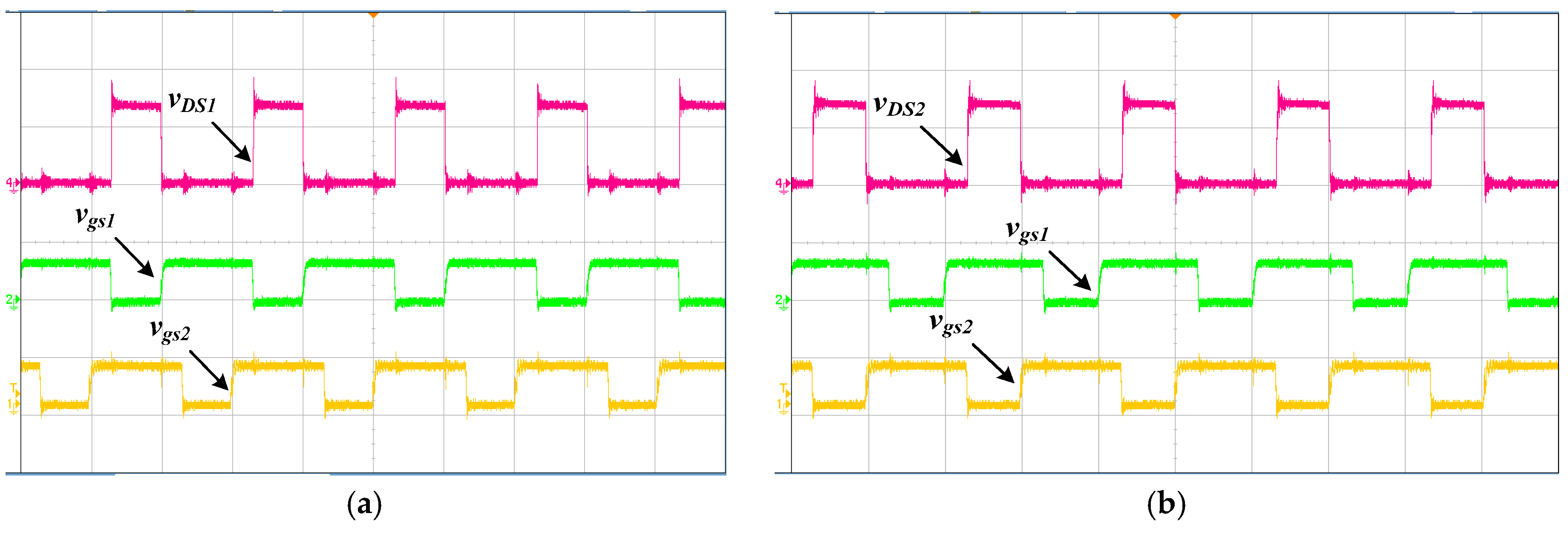
D3, the hyper-fast rectifier VS-8ETH03-1PbF (Nichicon, Kyoto, Japan) is considered, which has 1.25 V forward voltage and 35 ns reverse recovery time. The voltage waveforms of active power switches and control signals are shown in
Figure 4a,b, which indicate that the voltage across
S1 and
S2 are both near 65 V. This value also demonstrates a relatively low voltage stress across the active power semiconductor, as compared with other high step-up converters.
Figure 5a,d is the practical measurements of voltage waveforms of diodes
Do,
D1,
D2 and
D3, in turn, at the condition
D = 0.62 and in CCM operation.
Figure 5a illustrates that the maximum blocking voltage of
Do is nearly 200 V. With respect to
D1, its voltage stress approaches to 280 V, as shown in
Figure 5b. Diodes
D2 and
D3 endure the same voltage of 130 V. In
Figure 5, all the diode voltage stresses are in compliance with Equations (25)–(28).
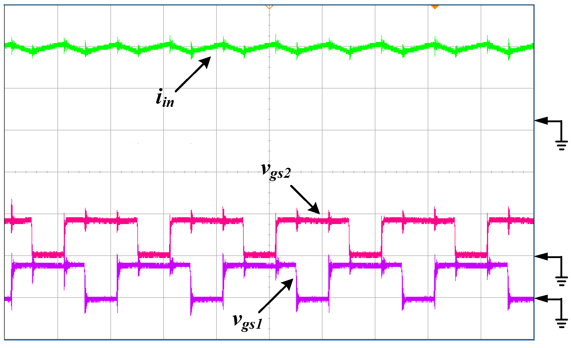
Figure 6 shows the waveforms of input current and the corresponding control signals. It indicates that the magnitude of input ripple current is limited to less than 2 A.
Figure 7 depicts the measured and simulated efficiencies from light load to full load. In the simulations, the considered conditions include forward voltage of diode,
RDS(on) of MOSFET, copper loss of the coupled inductor, switching loss of MOSFET, and the equivalent resistance of diode. The maximum value of the measured efficiency is 93.7% at
Po = 140 W.
Figure 8 is the photo of test bench, in which PV simulator Chroma 62050H-600S (Taoyuan, Taiwan) serves as input source, electronic load Chroma 6320 draws power from the converter, and all waveforms are measured by oscilloscope KEYSIGHT DSOX4024A (Santa Rosa, CA, USA).


