Article

Effect of Intrinsic Stress on Structural and Optical Properties of Amorphous Si-Doped SnO2 Thin-Film

1
Luminescent Materials and Devices, South China University of Technology, Guangzhou 510640, China
2
State Key Laboratory of Luminescence and Applications, Changchun Institute of Optics, Fine Mechanics and Physics, Changchun 130033, China
3
Integrated System for Laser Applications Group, Institute of Microelectronics of Chinese Academy of Sciences, Beijing 100029, China
*
Authors to whom correspondence should be addressed.
Materials 2017, 10(1), 24; https://doi.org/10.3390/ma10010024
Submission received: 13 September 2016 / Revised: 22 December 2016 / Accepted: 22 December 2016 / Published: 1 January 2017
(This article belongs to the Special Issue Oxide Semiconductor Thin-Film Transistor)

Abstract

:
The effect of intrinsic stress on the structure and physical properties of silicon-tin-oxide (STO) films have been investigated. Since a state of tensile stress is available in as-deposited films, the value of stress can be exponentially enhanced when the annealing temperature is increased. The tensile stress is able to not only suppress the crystallization and widen the optical band gap of STO films, but also reduce defects of STO films. In this report, the good electrical performance of STO thin-film transistors (TFTs) can be obtained when annealing temperature is 450 °C. This includes a value of saturation mobility that can be reached at 6.7 cm2/Vs, a ratio of Ion/Ioff as 7.34 × 10⁷, a steep sub-threshold swing at 0.625 V/decade, and a low trap density of 7.96 × 10¹¹ eV−1·cm−2, respectively.

Graphical Abstract

1. Introduction

In recent years, the display industry is undergoing a significant shift from rigid displays to flexible displays. Transparent amorphous oxide semiconductors for thin-film transistors (TFTs) have been attracting tremendous attentions due to their low-temperature manufacturing process, highly optical transparency, good uniformity of film deposition and low cost [1]. Generally, interfacial defects of oxide TFTs between the channel layer and the dielectric layer can be reduced at high annealing temperature in the manufacturing process. Besides, it is important for oxide TFTs to be embedded in Polyimide (PI) substrate with tolerable temperature up to 450 °C for flexible displays [2,3]. However, in practical applications, the various stresses (i.e., tensile stress and compressive stress) of the oxide semiconductor films on plastic substrates may cause the fracture because the bending or stretching in plane strain can be initiated during the process of the large-area films production [4,5,6]. Therefore, avoiding the fracture caused by stress-related effects (i.e., keeping the integrity and stability of devices) is critical for flexible applications.
In general, all thin films can be considered in a state of stress during the deposition process, leading to different electrical and optical properties [7]. Therefore, the relationship between the stress of oxide semiconductors film and their properties should be systematically studied. In this study, STO film instead of the well-known indium-gallium-zinc-oxide (IGZO) film is investigated due to some merits of STO films, such as no toxicity, controllable components, and low cost. In fact, STO films not only exhibit an n-type oxide semiconductor but also own strong chemical stability, leading to the fact that they can be fabricated on back-channel-etched type TFTs [8]. Previously, Zhang et al. revealed that STO films related to doping element (Si and N) effects on heavily p-type silicon substrate [9,10]. For the flexible electronic device, we need enlarge the research on different substrates and stress situation.
In this paper, it is the first time at different annealing temperatures have been investigated. Finally, the optical band that characterizations for structural and optical evolution related to intrinsic stress of the STO films have been reported. In addition, the stress of such film used for fabricating device on the flexible substrate gap, surface morphology and oxygen vacancies correlated with the stress in the STO films have been studied respectively.

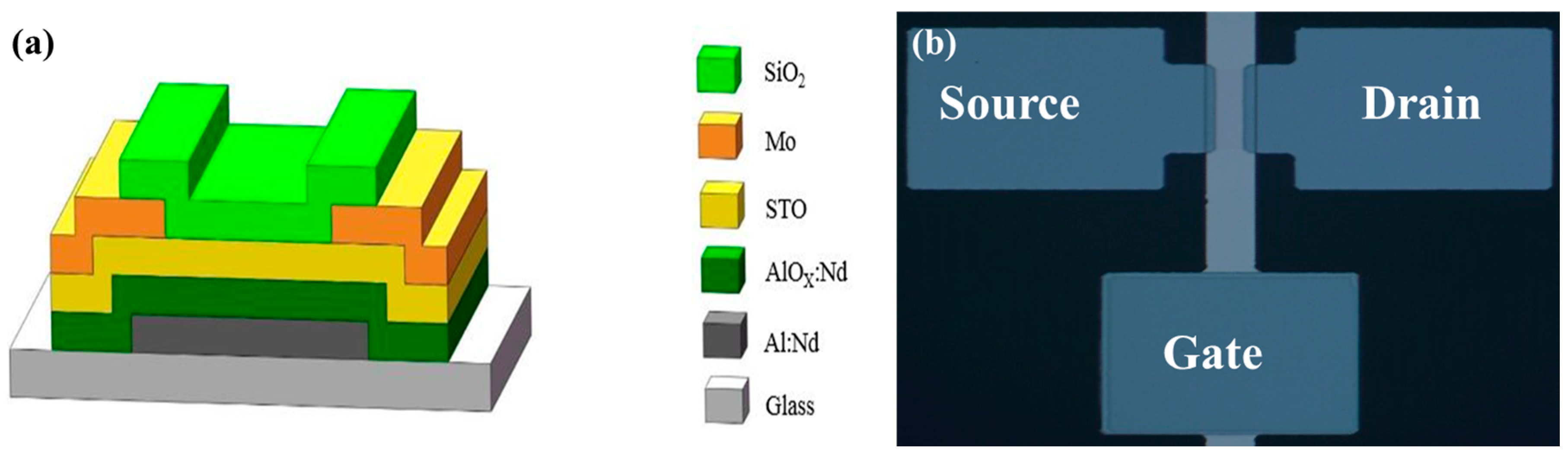
2. Experimental Methods

STO films are successively deposited on the surface of Si and glass substrate by radio frequency (RF) magnetron sputtering using an STO (SiO2:SnO2 = 5:95 wt %) target at room temperature. The power is 300 W, the ratio of Ar/O2 is 20:2 sccm with ambient pressure of 2 mTorr during the process. Finally, as-deposited STO films with thicknesses of 200 nm ought to be annealed at temperatures of 150, 250, 350 and 450 °C for 0.5 h on the hot plate, respectively.
To obtain STO TFTs with a bottom-gate inverted staggered-type structure (shown in Figure 1), a 300 nm Al-Nd alloy (3 wt % of Nd) as patterned gate metal can be firstly deposited by direct current (DC) magnetron sputtering. Subsequently, the film is anodized to form a 200 nm layer of AlOx:Nd on the surface in an electrolyte consisting of 3.68 wt % ammonium tartrate solution and ethylene glycol. Afterwards, a 5 nm STO thin film is deposited on the anodic oxide film by RF sputtering at room temperature. Then, for the source/drain (S/D) electrodes, a deposition of a metal film of Mo and a wet etched pattern have been processed in order to produce a channel with 100 μm width and 40 μm length when Phosphoric-Acetic-Nitric (70% Phosphoric acid, 10% Acetic acid, 5% Nitric acid) etchant is used. Finally, the post-annealing process of the device at 350 °C on a hot plate for 0.5 h is to be done before passivation of single-walled SiO2 films using plasma enhanced chemical vapor deposition (PECVD) at 250 °C.
The stress of STO films on Si substrate at different annealing temperatures has been characterized by the kSA Multi-beam Optical Sensor (MOS) system (KSA MOS Thermal Scan, k-Space Associates, Inc., Dexter, MI, USA). The structure and chemical state of STO films on glass substrate sare analyzed by X-ray diffraction (XRD) (Empyrean, PANalytical, Almelo, The Netherlands) and X-ray photoelectron spectroscopy (XPS) (Escalab 250 XI, Thermo Scientific, Waltham, MA, USA), respectively. The thicknesses of thin films are measured by a Dektak 150 surface profiler (Veeco, New York, NY, USA) and X-ray reflectivity (XRR). The surface morphology of films is obtained by atomic force microscopy (AFM) (XE-100, Eppendorf, Hamburg, Germany). The optical properties of the films are measured by a UV-3600 spectrophotometer (Shimadzu, Kyoto, Japan). The mobility and carrier concentration of the STO films are obtained by Hall-effect measurements (WAD (H.K) Co. Ltd., Hong Kong, China). The electrical characteristics of STO TFTs are examined in the dark using an Agilent 4155C semiconductor parameter analyzer (Agilent, Santa Clara, CA, USA) at room temperature.

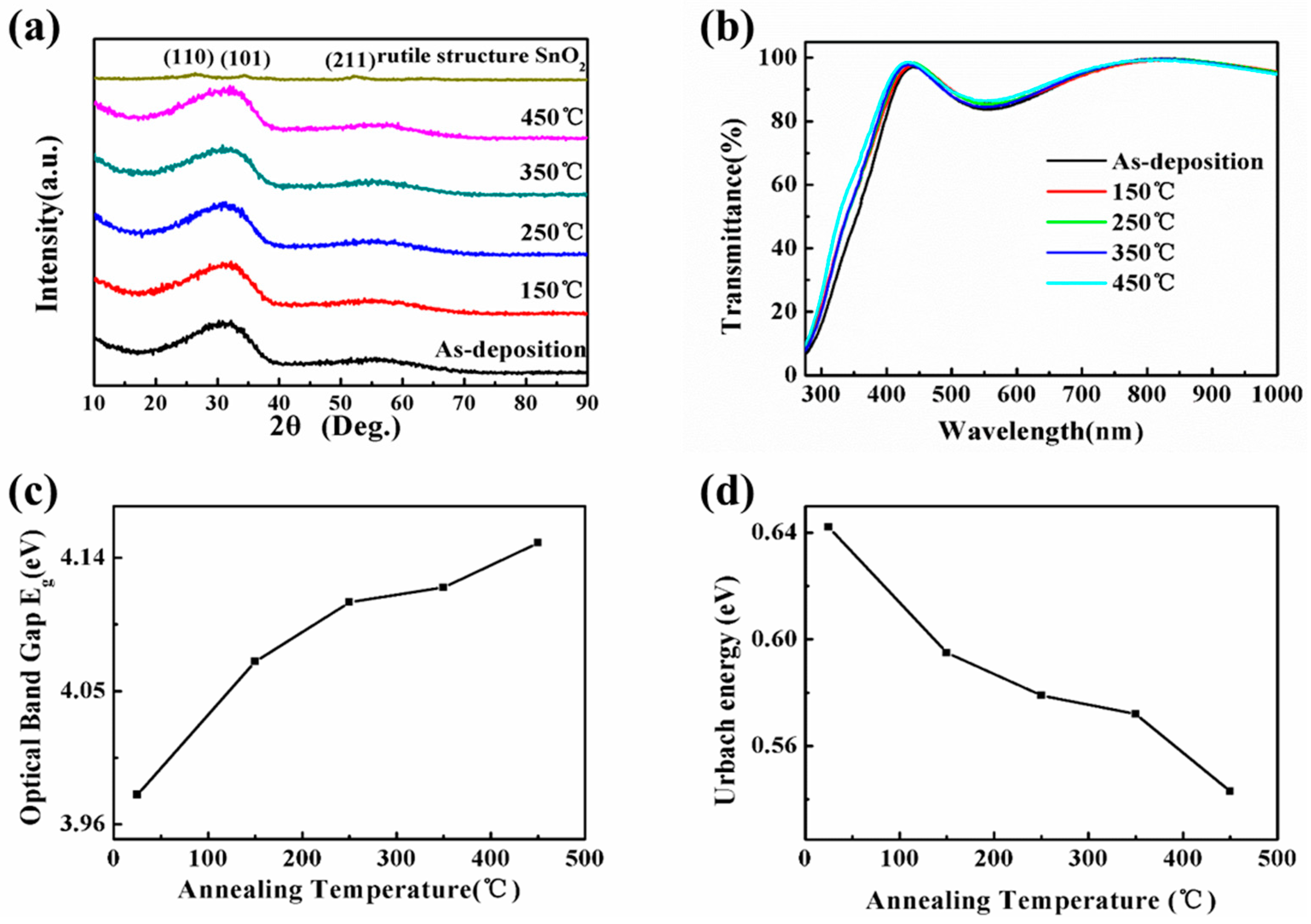
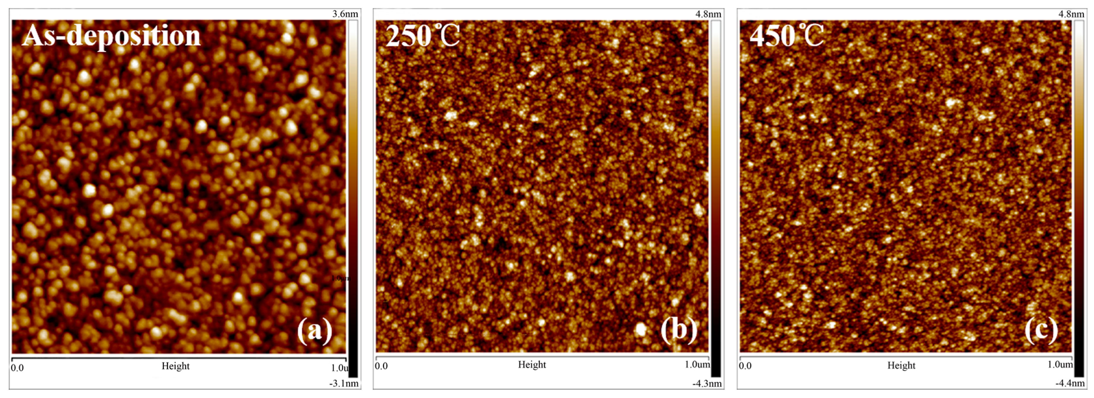
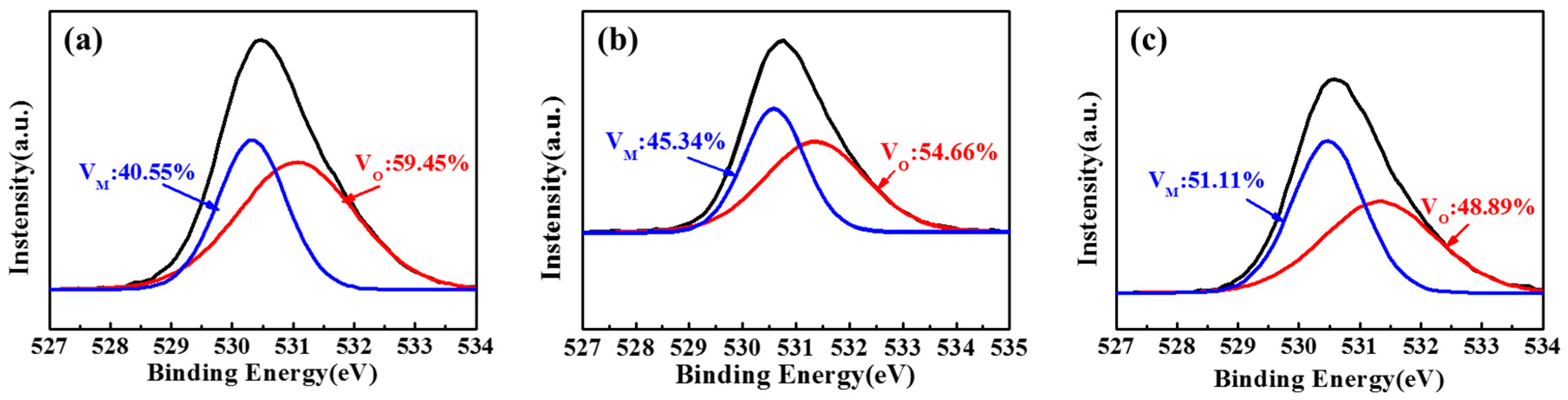
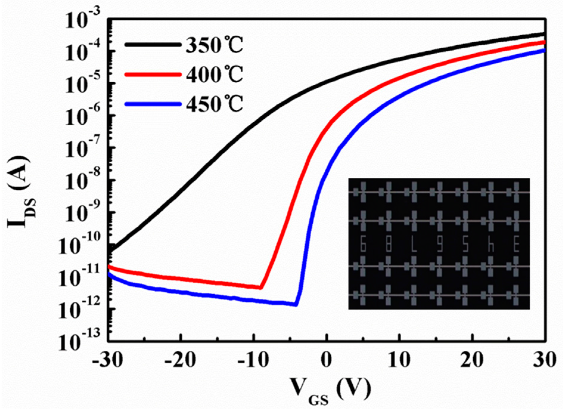
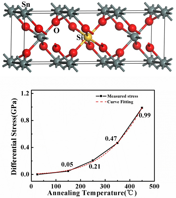
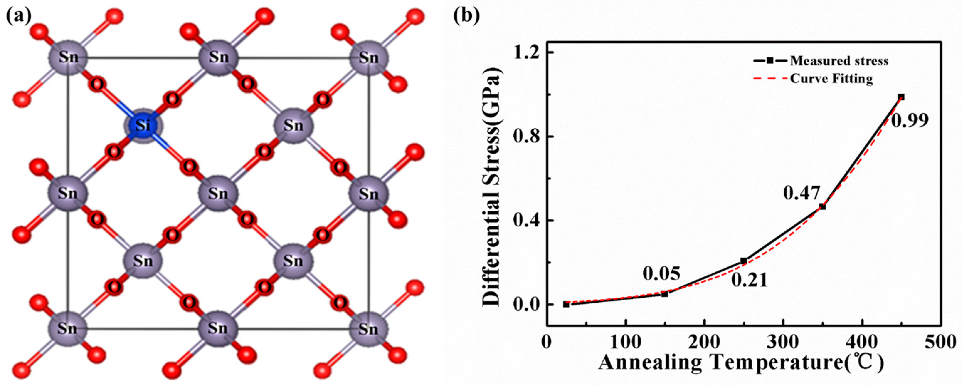
3. Results and Discussion

Generally, the stress of a film consists of intrinsic stress and extrinsic stress. The intrinsic stress is generated by the accumulating effect of defects because of the bombardment of the energetic species during deposition, while the extrinsic stress emerges due to lattice mismatch or different thermal expansion coefficients between the film and substrate materials. For all STO films, the extrinsic stress of such films can be avoidable because of excessive thickness [11], while their internal stress can be examined by comparing the radii of curvatures of the silicon substrates. Film stress ( σ ) is calculated according to Stoney’s Equation (1) [12]:
σ = ( d d 0 ) M s h s 2 cos α 12 h f L ,
where d 0 is initial spacing, d is the change in spacing, M s is biaxial modulus of the substrate, h s is the thickness of a substrate, h f is the thickness of a film, α is angle of incidence, and L is the distance from substrate to Camera CCD. In Figure 2b, the results of differential stress of STO films are proportional to annealing temperature from 25 to 450 °C. Moreover, good empirical fitting indicates that such STO films are in stretched states. The empirical fitting equation for STO thin films can be expressed below:
Δ σ = e x p ( 4.77206 + 0.01474 T 9.26126 × 10 6 T 2 ) ,
where ( Δ σ ) is differential stress, and T is annealing temperature. In order to understand the relationship between the structural properties of STO films and their corresponding stresses at different annealing temperatures, the XRD characterization is used. In Figure 3a, it is known that the SnO2 film exhibits typical rutile structure and the three peaks are at 26.6°, 33.8° and 51.8°, corresponding to the (110), (101) and (211) crystallographic planes, respectively. Notably, its crystalline structure has already been transformed into the amorphous structure when a small amount of Si infiltrates the SnO2 lattice (shown in Figure 2a). The STO films maintain their amorphous structure when annealing temperature is increased because the direction of crystallization of film is disordered by the increased tensile stress, resulting in the good uniformity over large areas and unchanged electrical properties. Figure 3b shows the transmittance spectra of STO films at different annealing temperatures in the wavelength ranging from 300 to 1000 nm. The average transmittance of all STO films is in the visible range of 80%. The optical band gap ( E g ) can be calculated by the Tauc equation as follows:
( a h v ) 2 = A ( h v E g ) ,
where a is the absorption coefficient, h is the Planck’s constant, v is the frequency of theincidentphoton and A is the energy-independent constant [13]. The E g can be obtained by extrapolating the linear part of ( a h v ) 2 versus h v for all samples to the energy axis. The value of band gap ( E g ) increases from 3.98 to 4.15 eV as the annealing temperature increased from 25 to 450 °C (Figure 3c). The change of E g can be mainly attributed to two factors: the local ordering and the stress. On one hand, atoms with thermal energy can be reordered in the STO films by the annealing process. This improves the local ordering and leads to the change of E g . On the other hand, the repulsion between the oxygen 2p and the tin 5s bands is decreased when STO films are in stretched states [14]. As a result, the optical band gap is widened. Furthermore, there is a reduction for structural defects of the film at high annealing temperature (shown in Figure 3d). The Urbach energy ( E u ) is an empirical parameter representing structural defects and can be extracted from the absorption coefficient [15,16]. The E u is extracted using Equation (4):
α = α 0 e x p ( h v E u ) ,
where α 0 is the pre-exponential factor. It is clearly observed that the value of E u displays a declining pattern.
In general, the intrinsic stress originated from the structural defects such as dislocations, nonstoichiometric components, and oxygen vacancies can be decreased when the annealing temperature is increased for a film. However, for STO films, the intrinsic stress is performed in a completely opposite manner due to two reasons: (1) the verification of the improvement of the tensile stress by increasing the density when the vertical thickness of STO films is shrunk (details are shown in Table 1). Moreover, the high tensile stress will further facilitate the carrier mobility due to greater overlapping of s-orbitals of the cations in STO films [17]; (2) the microstructure of the as-deposited STO films becomes more compact as the annealing temperature starts to increase. It is confirmed by surface morphologies of STO films using AFM characterization that the tensile stress is increased when the interaction of atoms is strengthened at annealing temperature of 250 and 450 °C.
In Figure 4, a large amount of round-shaped particle-like structures for the surface morphology of the as-deposited STO films starts to disappear when annealing temperature is increased up to 450 °C. Such behavior of formation and morphology for STO films is exhibited due to their dependence on interfacial energy [18]. It is also known that the defect states such as grain-like structure at low annealing temperature impacts the charge carriers’ transmission [19].
Figure 5 shows the XPS spectra of STO films in the O1 regions. The O1 peaks are divided into two principal peaks using a Gaussian–Lorentzian profile. The bind energy peak at 530.4 eV is attributed to M-O-M (VM) in the oxide lattices without oxygen defects, while the peak centered at 531.3 eV is assigned to the oxygen vacancies (VO). In general, the charge carriers in the oxide semiconductors are related to oxygen vacancies that donate two free electrons as shallow donors in STO films. The defects and the high carrier density of STO films will be suppressed at a high level state of tensile stress. The VO of the STO films is decreased from 59.45% to 48.89% as the annealing temperature rises up to 450 °C.
In summary, STO TFTs is fabricated through optimized process. Figure 6 shows the transfer characteristic curves of STO TFTs with different annealing temperatures. The curves were measured at V G S = 30.1 V. The electrical performances of TFT are improved effectively by processing at different annealing temperature (shown in Table 2). The saturation mobility μ s a t is calculated by the following Equation (5) [20]:
μ s a t = ( d I D S d V G S ) 2 1 2 C i W L ,
where I D S and V G S are the drain current and drain voltage, respectively. C i is the gate capacitance per unit area. The trap density ( D t ) of the bulk states or the interface states between STO films and the dielectric interface can be calculated using the following Equation (6) [21]:
D t = [ S S l o g ( e ) k B T q 1 ] C i q ,
where k B is Boltzmann constant, T is absolute temperature, C i is the capacitance per unit area, q is a unit charge, and S S is sub-threshold swing. As shown in Table 2, STO TFTs do not exhibit switching behavior at annealing temperature of 350 °C. However, when the device is annealed at 400 °C, the performances of μ s a t , Von, Ion/Ioff ratio, S S and D t are 8.03 cm2/Vs, −9 V, 4.18 × 10⁷, 1.41 V/decade and 2.28 × 10¹² eV−1·cm−2, respectively. When the annealing process is at a temperature of 450 °C, the performances of a μ s a t , Von, Ion/Ioff ratio, S S and D t are 6.7 cm2/Vs, −4.8 V, 7.34 × 10⁷, 0.625 V/decade and 7.96 × 10¹¹ eV−1·cm−2, respectively. From the above results, it is obviously observed that the oxygen vacancies and the trap states can be effectively reduced, and better electrical performances can be obtained at a high annealing temperature of 450 °C.

4. Conclusions

The relationship between the stress and optical band gap, the surface morphology and the oxygen vacancies of STO films at different annealing temperatures have been systematically investigated. It is found that STO films exhibit tensile stress, which increases exponentially with the rise of annealing temperature. In addition, the control of tensile stress of STO film is implemented by the annealing process. The tensile stress can suppress the crystallization and widen the optical band gap of STO films, and also minimize the defects in STO films. STO TFTs annealed at 450 °C exhibit better performance, with a saturation mobility of 6.7 cm2/Vs, a high Ion/Ioff ratio of 7.34 × 10⁷, a steep sub-threshold swing of 0.625 V/decade and a low trap density of 7.96 × 10¹¹ eV−1·cm−2. These results suggest that the STO film is a promising active layer for transparent flexible displays.

Acknowledgments

This work was supported by the National Key Research and Development Program of China (No. 2016YFB0401504 and 2016YFF0203603), the National Natural Science Foundation of China (61307077, 61376083), the China Postdoctoral Science Foundation (2015T80080), the National Key Basic Research and Development Program of China (973 program, Grant No. 2015CB655004) founded by MOST, the Guangdong Natural Science Foundation (No. 2016A030313459), the Science and Technology Project of Guangdong Province (No. 2014B090915004, 2016B090907001, 2014A040401014, 2016B090906002, 2015A010101323, 2014B090916002, 2015A010101323, 2015B090915001 and 2015B090914003), the Educational Commission of Guangdong Province (No. 2014KZDXM010 and 2015KTSCX003), the Fundamental Research Funds for the Central Universities (No. 2015ZP024 and 2015ZZ063), and the State Key Laboratory of Luminescence and Applications (SKLA-2016-11).

Author Contributions

Rihui Yao, Honglong Ning, Zichen Zhang and Xianzhe Liu conceived and designed the experiments; Xianzhe Liu and Hongke Zhang performed the experiments; Zhiqiang Fang, Wei Cai and Jianqiu Chen analyzed the data; Miao Xu, Lei Wang, LinfengLan, Junbiao Peng and Xiaofeng Wang provided valuable discussions and suggestions; Honglong Ning, Xianzhe Liu and Zichen Zhang wrote the paper.

Conflicts of Interest

The authors declare no conflict of interest.

References

  1. Nomura, K.; Ohta, H.; Takagi, A.; Kamiya, T.; Hirano, M.; Hosono, H. Room-temperature fabrication of transparent flexible thin-film transistors using amorphous oxide semiconductors. Nature 2004, 432, 488. [Google Scholar] [CrossRef] [PubMed]
  2. Gao, X.; Lin, L.; Liu, Y.; Huang, X. LTPS TFT process on polyimide substrate for flexible AMOLED. IEEE/OSA J. Disp. Technol. 2015, 11, 666. [Google Scholar] [CrossRef]
  3. Xiao, P.; Dong, T.; Lan, L.; Lin, Z.; Song, W.; Song, E.; Sun, S.; Li, Y.; Gao, P.; Luo, D.; et al. High-mobility flexible thin-film transistors with a low-temperature zirconium-doped indium oxide channel layer. Phys. Status Solidi 2016, 10, 493–497. [Google Scholar] [CrossRef]
  4. Gadre, M.J.; Alford, T.L. Highest transmittance and high-mobility amorphous indium gallium zinc oxide films on flexible substrate by room-temperature deposition and post-deposition anneals. Appl. Phys. Lett. 2011, 99, 051901. [Google Scholar] [CrossRef]
  5. Park, J.S.; Kim, T.W.; Stryakhilev, D.; Lee, J.S.; An, S.G.; Pyo, Y.S.; Lee, D.B.; Mo, Y.G.; Jin, D.U.; Chung, H.K. Flexible full color organic light-emitting diode display on polyimide plastic substrate driven by amorphous indium gallium zinc oxide thin-film transistors. Appl. Phys. Lett. 2009, 95, 013503. [Google Scholar] [CrossRef]
  6. Iwamatsu, S.; Takechi, K.; Yahagi, T.; Abe, Y.; Tanabe, H.; Kobayashi, S. Fabrication of suspended amorphous indium–gallium–zinc oxide thin-film transistors using bulk micromachining techniques. Jpn. J. Appl. Phys. 2014, 53, 066503. [Google Scholar] [CrossRef]
  7. Thornton, J.A. Stress-related effects in thin films. Thin Solid Films 1989, 171, 5–31. [Google Scholar] [CrossRef]
  8. Liu, X.; Cai, W.; Chen, J.; Fang, Z.; Ning, H.; Hu, S.; Tao, R.; Zeng, Y.; Zheng, Z.; Yao, R.; et al. A novel nondestructive testing method for amorphous Si–Sn–O films. J. Phys. D Appl. Phys. 2016, 49, 505102. [Google Scholar] [CrossRef]
  9. Yang, J.; Yang, Z.; Meng, T.; Han, Y.; Wang, X.; Zhang, Q. Effects of silicon doping on the performance of tin oxide thin film transistors. Phys. Status Solidi A 2015, 213, 1010–1015. [Google Scholar] [CrossRef]
  10. Yang, J.; Han, Y.; Fu, R.; Zhang, Q. Effects of nitrogen doping on performance of amorphous SnSiO thin film transistor. J. Disp. Technol. 2016. [Google Scholar] [CrossRef]
  11. Kumar, R.; Khare, N.; Kumar, V.; Bhalla, G.L. Effect of intrinsic stress on the optical properties of nanostructured ZnO thin films grown by rf magnetron sputtering. Appl. Surf. Sci. 2008, 254, 6509–6513. [Google Scholar] [CrossRef]
  12. Lee, H.W.; Lau, S.P.; Wang, Y.G.; Tay, B.K.; Hng, H.H. Internal stress and surface morphology of zinc oxide thin films deposited by filtered cathodic vacuum arc technique. Thin Solid Films 2004, 458, 15–19. [Google Scholar] [CrossRef]
  13. Tauc, J.; Grigorovici, R.; Vancu, A. Optical properties and electronic structure of amorphous germanium. Phys. Status Solidi 1966, 15, 627–637. [Google Scholar] [CrossRef]
  14. Ghosh, R.; Basak, D.; Fujihara, S. Effect of substrate-induced strain on the structural, electrical, and optical properties of polycrystalline ZnO thin films. J. Appl. Phys. 2004, 96, 2689–2692. [Google Scholar] [CrossRef]
  15. Malek, M.F.; Mamat, M.H.; Musa, M.Z.; Soga, T.; Rahman, S.A.; Alrokayan, S.A.H.; Khan, H.A.; Rusop, M. Metamorphosis of strain/stress on optical band gap energy of ZAO thin films via manipulation of thermal annealing process. J. Lumin. 2015, 160, 165–175. [Google Scholar] [CrossRef]
  16. Zaynobidinov, S.; Ikramov, R.G.; Jalalov, R.M. Urbach energy and the tails of the density of states in amorphous semiconductors. J. Appl. Spectrosc. 2011, 78, 223–227. [Google Scholar] [CrossRef]
  17. Kaczmarski, J.; Boll, T.; Borysiewicz, M.A.; Taube, A.; Thuvander, M.; Law, J.Y.; Kamińska, E.; Stiller, K. Controlling In–Ga–Zn–O thin films transport properties through density changes. Thin Solid Films 2016, 608, 57–61. [Google Scholar] [CrossRef]
  18. Lin, Y.; Xie, J.; Wang, H.; Li, Y.; Chavez, C.; Lee, S.; Foltyn, S.R.; Crooker, S.A.; Burrell, A.K.; McCleskey, T.M.; et al. Green luminescent zinc oxide films prepared by polymer-assisted deposition with rapid thermal process. Thin Solid Films 2005, 492, 101–104. [Google Scholar] [CrossRef]
  19. Ellmer, K. Resistivity of polycrystalline zinc oxide films: Current status and physical limit. J. Phys. D Appl. Phys. 2001, 34, 3097. [Google Scholar] [CrossRef]
  20. Kamiya, T.; Nomura, K.; Hosono, H. Present status of amorphous In–Ga–Zn–O thin-film transistors. Sci. Technol. Adv. Mater. 2010, 11, 44305. [Google Scholar] [CrossRef] [PubMed]
  21. Liu, X.; Ning, H.; Chen, J.; Cai, W.; Hu, S.; Tao, R.; Zeng, Y.; Zheng, Z.; Yao, R.; Xu, M.; et al. High-performance back-channel-etched thin-film transistors with amorphous Si-incorporated SnO2 active layer. Appl. Phys. Lett. 2016, 108, 112106. [Google Scholar] [CrossRef]
Figure 1. (a) Cross-sectional schematic of STO TFT; (b) Micrograph of STO TFT (Width/Length = 100 µm/40 µm).
Materials 10 00024 g001
Figure 2. (a) The schematic structure of STO films; (b) The differential stress of STO films annealed at different temperatures. The red dash line represents an exponential curve fitting well with the experimental data.
Materials 10 00024 g002
Figure 3. (a) XRD patterns; (b) Transmittance; (c) Band gap ( E g ); and (d) Urbach energy ( E u ) of 200 nm thick STO thin film annealed at different temperatures.
Materials 10 00024 g003
Figure 4. AFM images (1 × 1 μm) of STO films annealed at different temperatures: (a) As-deposition; (b) 250 °C and (c) 450 °C in air for 0.5 h.
Materials 10 00024 g004
Figure 5. The O1 region of XPS spectra for STO films with different annealing temperatures: (a) As-deposition; (b) 250 °C; (c) 450 °C, respectively.
Materials 10 00024 g005
Figure 6. Transfer characteristic curves of STO TFTs annealed at 350, 400, and 450 °C, respectively.
Materials 10 00024 g006
Table 1. The summary of Hall mobility, carrier density, and density for STO films annealed at different temperatures.
Annealing Temperature
(°C)
Carrier Mobility
(cm2/Vs)
Carrier Density
(cm−3)
Density
(g/cm3)
Roughness
(nm)
As-deposition4.704.09 × 10185.7230.75
1505.667.86 × 10185.7500.18
2503.325.76 × 10195.8220.19
3506.625.43 × 10196.0760.09
4506.531.72 × 10196.2500.09
Table 2. Device parameters of STO TFTs.
Annealing Temperature
(°C)
μ s a t
(cm2/Vs)
Von
(V)
Ion/Ioff S S
(V/decade)
D t
(eV−1·cm−2)
350--<−30------
4008.03−94.18 × 1071.412.28 × 1012
4506.7−4.87.34 × 1070.6257.96 × 1011

