On the Hole Injection for III-Nitride Based Deep Ultraviolet Light-Emitting Diodes


Abstract
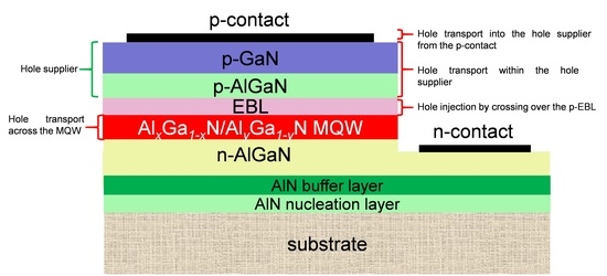
1. Introduction
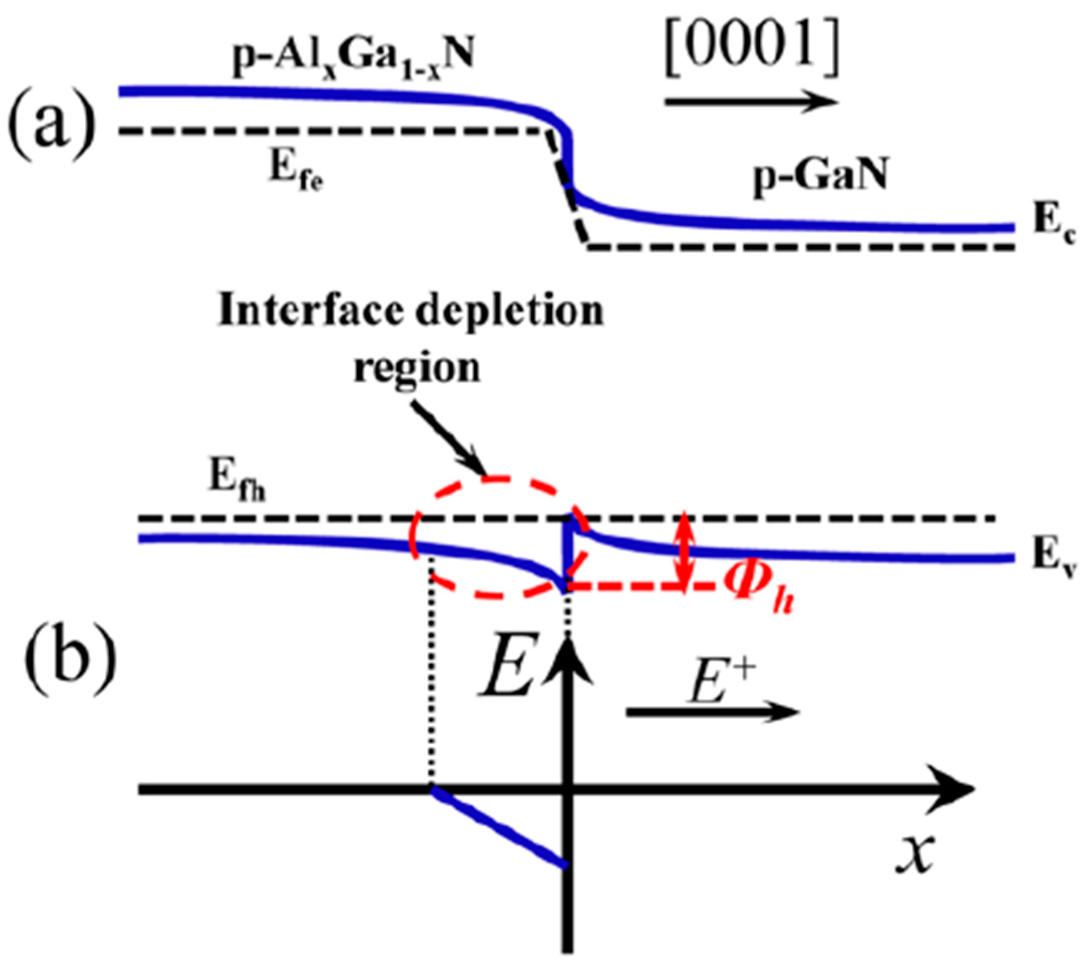
2. Increase the Hole Injection Efficiency from the p-Type Ohmic Contact into the Hole Supplier
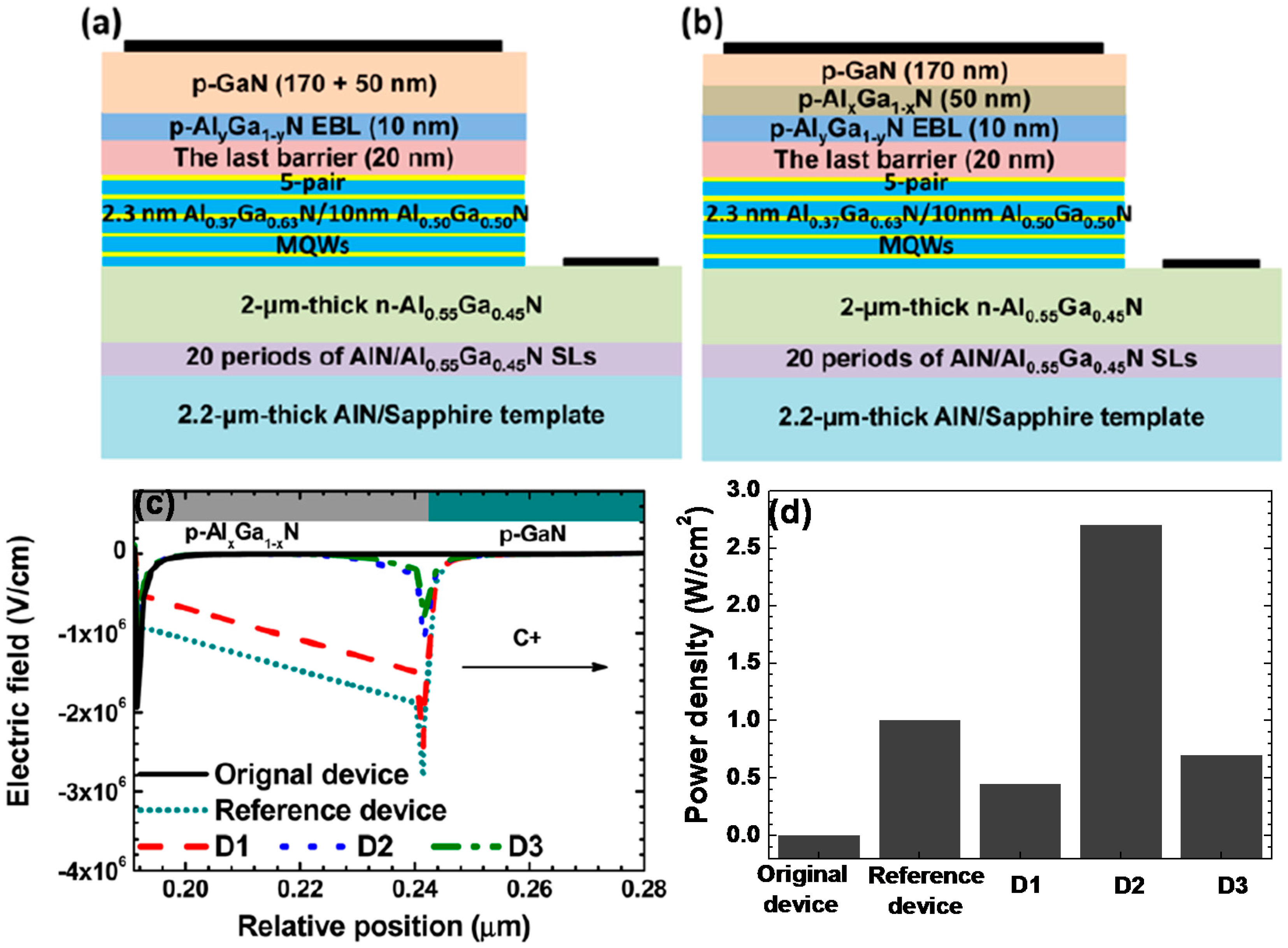
3. Enhance the Hole Transport within the Hole Supplier
4. Reduce the Hole Blocking Effect by the p-EBL
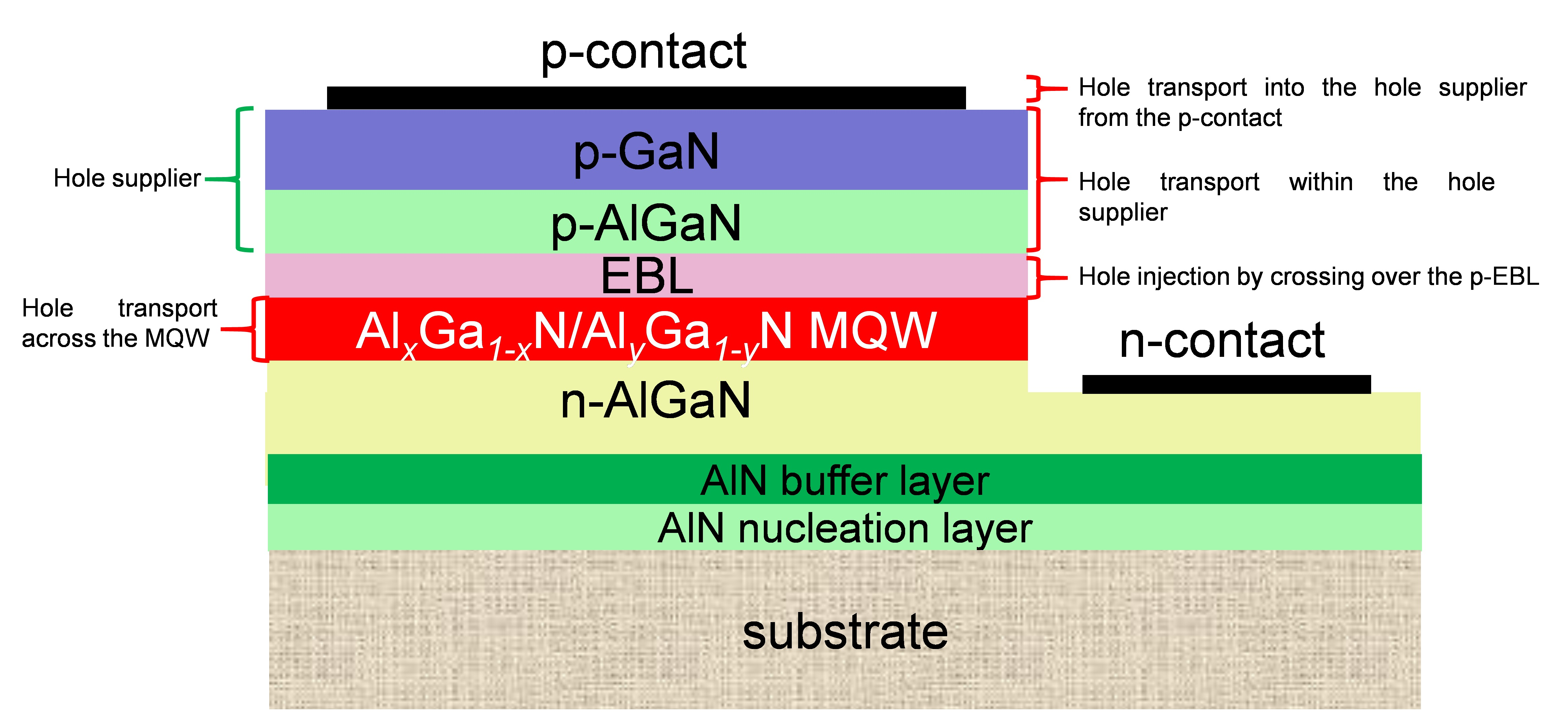
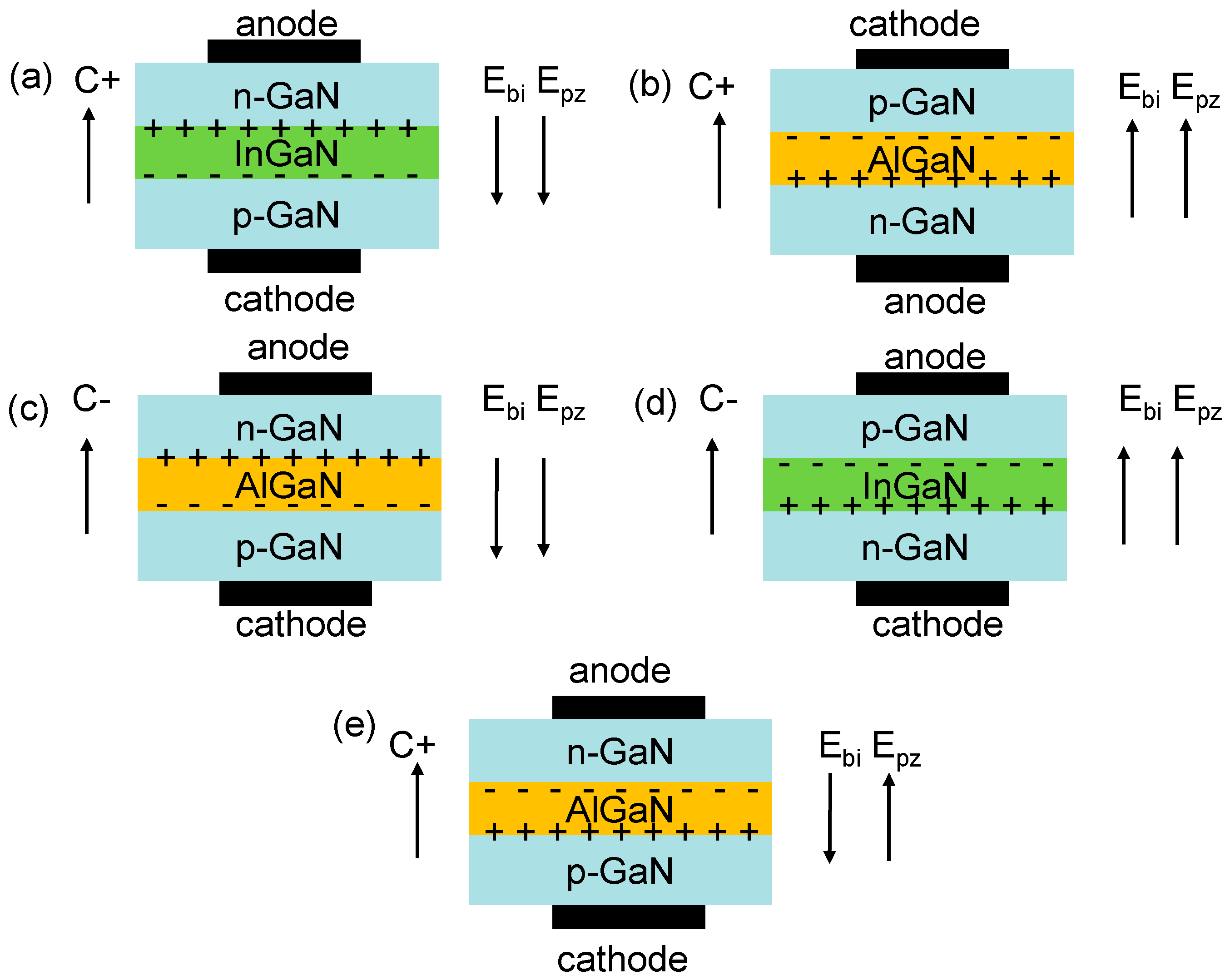
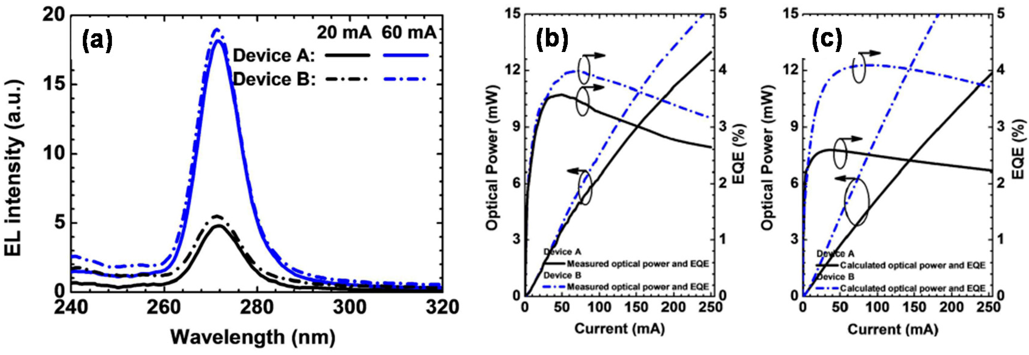
5. Increase the Hole Concentration in the MQW Region
6. Summary
Acknowledgments
Conflicts of Interest
References
- Khan, A.; Balakrishnan, K.; Katona, T. Ultraviolet light-emitting diodes based on group three nitrides. Nat. Photonics 2008, 2, 77–84. [Google Scholar] [CrossRef]
- Park, J.S.; Kim, J.K.; Cho, J.; Seong, T.Y. Review-group III-nitride-based ultraviolet light-emitting diodes: Ways of increasing xxternal quantum efficiency. ECS J. Solid State Sci. Technol. 2017, 6, Q42–Q52. [Google Scholar] [CrossRef]
- Kneissl, M.; Kolbe, T.; Chua, C.; Kueller, V.; Lobo, N.; Stellmach, J.; Knauer, A.; Rodriguez, H.; Einfeldt, S.; Yang, Z.; et al. Advances in group III-nitride-based deep UV light-emitting diode technology. Semicond. Sci. Technol. 2011, 26, 014036. [Google Scholar] [CrossRef]
- Nam, K.B.; Li, J.; Nakarmi, M.L.; Lin, J.Y.; Jiang, H.X. Unique optical properties of AlGaN alloys and related ultraviolet emitters. Appl. Phys. Lett. 2004, 84, 5264–5266. [Google Scholar] [CrossRef]
- Wang, W.Y.; Lu, H.M.; Fu, L.; He, C.G.; Wang, M.X.; Tang, N.; Xu, F.J.; Yu, T.J.; Ge, W.K.; Shen, B. Enhancement of optical polarization degree of AlGaN quantum wells by using staggered structure. Opt. Express 2016, 24, 18176–18183. [Google Scholar] [CrossRef] [PubMed]
- Lu, H.M.; Yu, T.J.; Yuan, G.C.; Chen, X.J.; Chen, Z.Z.; Chen, G.X.; Zhang, G.Y. Enhancement of surface emission in deep ultraviolet AlGaN-based light emitting diodes with staggered quantum wells. Opt. Lett. 2012, 37, 3693–3695. [Google Scholar] [CrossRef] [PubMed]
- Lu, H.M.; Yu, T.J.; Chen, X.J.; Wang, J.P.; Zhang, G.Y. Band engineering for surface emission enhancement in Al-rich AlGaN-based deep-ultraviolet light emitting diodes. Jpn. J. Appl. Phys. 2016, 55, 05FJ12. [Google Scholar] [CrossRef]
- Kuo, Y.; Su, C.-Y.; Hsieh, C.; Chang, W.-Y.; Huang, C.-A.; Kiang, Y.-W.; Yang, C.C. Surface plasmon coupling for suppressing p-GaN absorption and TM-polarized emission in a deep-UV light-emitting diode. Opt. Lett. 2015, 40, 4229–4232. [Google Scholar] [CrossRef] [PubMed]
- Ryu, H.Y.; Choi, I.G.; Choi, H.S.; Shim, J.I. Investigation of light extraction efficiency in AlGaN deep-ultraviolet light-emitting diodes. Appl. Phys. Express 2013, 6, 062101. [Google Scholar] [CrossRef]
- Shatalov, M.; Sun, W.; Lunev, A.; Hu, X.; Dobrinsky, A.; Bilkenko, Y.; Yang, J.; Shur, M.; Gaska, R.; Moe, C.; et al. AlGaN deep-ultraviolet light-emitting eiodes with external quantum efficiency above 10%. Appl. Phys. Express 2012, 5, 082101. [Google Scholar] [CrossRef]
- Zhang, Z.-H.; Zhang, Y.H.; Bi, W.G.; Demir, H.V.; Sun, X.W. On the internal quantum efficiency for InGaN/GaN light-emitting diodes grown on insulating substrates. Phys. Status Solidi A 2016, 213, 3078–3102. [Google Scholar] [CrossRef]
- Imura, M.; Nakano, K.; Fujimoto, N.; Okada, N.; Balakrishnan, K.; Iwaya, M.; Kamiyama, S.; Amano, H.; Akasaki, I.; Noro, T.; et al. Dislocations in AIN epilayers grown on sapphire substrate by high-temperature metal-organic vapor phase epitaxy. Jpn. J. Appl. Phys. 2007, 46, 1458–1462. [Google Scholar] [CrossRef]
- Hirayama, H. Advances of AlGaN-based high-efficiency deep-UV LEDs. In Proceedings of the Communications and Photonics Conference and Exhibition (ACP), 2010 Asia, Shanghai, China, 8–12 December 2010. [Google Scholar] [CrossRef]
- Hammersley, S.; Watson-Parris, D.; Dawson, P.; Godfrey, M.J.; Badcock, T.J.; Kappers, M.J.; McAleese, C.; Oliver, R.A.; Humphreys, C.J. The consequences of high injected carrier densities on carrier localization and efficiency droop in InGaN/GaN quantum well structures. J. Appl. Phys. 2012, 111, 083512. [Google Scholar] [CrossRef]
- Iveland, J.; Martinelli, L.; Peretti, J.; Speck, J.S.; Weisbuch, C. Direct measurement of auger electrons emitted from a semiconductor light-emitting diode under electrical injection: Identification of the dominant mechanism for efficiency droop. Phys. Rev. Lett. 2013, 110, 177406. [Google Scholar] [CrossRef] [PubMed]
- Piprek, J. Efficiency droop in nitride-based light-emitting diodes. Phys. Status Solidi A 2010, 207, 2217–2225. [Google Scholar] [CrossRef]
- Sun, W.; Shatalov, M.; Deng, J.; Hu, X.; Yang, J.; Lunev, A.; Bilenko, Y.; Shur, M.; Gaska, R. Efficiency droop in 245–247 nm AlGaN light-emitting diodes with continuous wave 2 mW output power. Appl. Phys. Lett. 2010, 96, 061102. [Google Scholar] [CrossRef]
- Banal, R.G.; Taniyasu, Y.; Yamamoto, H. Deep-ultraviolet light emission properties of nonpolar M-plane AlGaN quantum wells. Appl. Phys. Lett. 2014, 105, 053104. [Google Scholar] [CrossRef]
- Satter, M.M.; Lochner, Z.; Ryou, J.H.; Shen, S.C.; Dupuis, R.D.; Yoder, P.D. Polarization matching in AlGaN-based multiple-quantum-well deep ultraviolet laser diodes on AlN substrates using quaternary AlInGaN barriers. J. Lightwave Technol. 2012, 30, 3017–3025. [Google Scholar] [CrossRef]
- Li, L.; Miyachi, Y.; Miyoshi, M.; Egawa, T. Enhanced emission efficiency of deep ultraviolet light-emitting AlGaN multiple quantum wells grown on an N-AlGaN underlying layer. IEEE Photonics J. 2016, 8, 1601710. [Google Scholar] [CrossRef]
- Katsuragawa, M.; Sota, S.; Komori, M.; Anbe, C.; Takeuchi, T.; Sakai, H.; Amano, H.; Akasaki, I. Thermal ionization energy of Si and Mg in AlGaN. J. Cryst. Growth 1998, 189, 528–531. [Google Scholar] [CrossRef]
- Nakamura, S.; Mukai, T.; Senoh, M.; Iwasa, N. Thermal annealing effects on p-Type Mg-doped GaN films. Jpn. J. Appl. Phys. 1992, 31, L139–L142. [Google Scholar] [CrossRef]
- Hiroshi, A.; Masahiro, K.; Kazumasa, H.; Isamu, A. P-Type conduction in Mg-doped GaN treated with low-energy electron beam irradiation (LEEBI). Jpn. J. Appl. Phys. 1989, 28, L2112–L2114. [Google Scholar] [CrossRef]
- Zhang, Z.-H.; Chen, S.-W.H.; Zhang, Y.; Li, L.; Wang, S.-W.; Tian, K.; Chu, C.; Fang, M.; Kuo, H.-C.; Bi, W. Hole transport manipulation to improve the hole injection for deep ultraviolet light-emitting diodes. ACS Photonics 2017, 4, 1846–1850. [Google Scholar] [CrossRef]
- Kim, M.; Fujita, T.; Fukahori, S.; Inazu, T.; Pernot, C.; Nagasawa, Y.; Hirano, A.; Ippommatsu, M.; Iwaya, M.; Takeuchi, T.; et al. AlGaN-based deep ultraviolet light-Emitting diodes fabricated on patterned sapphire substrates. Appl. Phys. Express 2011, 4, 092102–092103. [Google Scholar] [CrossRef]
- Dong, P.; Yan, J.C.; Zhang, Y.; Wang, J.X.; Zeng, J.P.; Geng, C.; Cong, P.P.; Sun, L.L.; Wei, T.B.; Zhao, L.X.; et al. AlGaN-based deep ultraviolet light-emitting diodes grown on nano-patterned sapphire substrates with significant improvement in internal quantum efficiency. J. Cryst. Growth 2014, 395, 9–13. [Google Scholar] [CrossRef]
- Wang, H.-M.; Zhang, J.-P.; Chen, C.-Q.; Fareed, Q.; Yang, J.-W.; Khan, M.A. AlN/AlGaN superlattices as dislocation filter for low-threading-dislocation thick AlGaN layers on sapphire. Appl. Phys. Lett. 2002, 81, 604–606. [Google Scholar] [CrossRef]
- Zhang, J.P.; Wang, H.M.; Gaevski, M.E.; Chen, C.Q.; Fareed, Q.; Yang, J.W.; Simin, G.; Khan, M.A. Crack-free thick AlGaN grown on sapphire using AlN/AlGaN superlattices for strain management. Appl. Phys. Lett. 2002, 80, 3542–3544. [Google Scholar] [CrossRef]
- Kinoshita, T.; Hironaka, K.; Obata, T.; Nagashima, T.; Dalmau, R.; Schlesser, R.; Moody, B.; Xie, J.Q.; Inoue, S.; Kumagai, Y.; et al. Deep-ultraviolet light-emitting diodes fabricated on AlN substrates prepared by hydride vapor phase epitaxy. Appl. Phys. Express 2012, 5, 122101. [Google Scholar] [CrossRef]
- Zhang, J.P.; Kuokstis, E.; Fareed, Q.; Wang, H.M.; Yang, J.W.; Simin, G.; Khan, M.A.; Tamulaitis, G.; Kurilcik, G.; Jursenas, S.; et al. Pulsed atomic layer epitaxy of quaternary AlInGaN layers for ultraviolet light emitters. Phys. Status Solidi A 2001, 188, 95–99. [Google Scholar] [CrossRef]
- Zhang, J.P.; Khan, M.A.; Sun, W.H.; Wang, H.M.; Chen, C.Q.; Fareed, Q.; Kuokstis, E.; Yang, J.W. Pulsed atomic-layer epitaxy of ultrahigh-quality AlxGa1-xN structures for deep ultraviolet emissions below 230 nm. Appl. Phys. Lett. 2002, 81, 4392–4394. [Google Scholar] [CrossRef]
- Iida, K.; Watanabe, H.; Takeda, K.; Nagai, T.; Sumii, T.; Nagamatsu, K.; Kawashima, T.; Balakrishnan, K.; Iwaya, M.; Kamiyama, S.; et al. High-efficiency AlGaN based UV emitters grown on high-crystalline-quality AlGaN using grooved AlN layer on sapphire substrate. Phys. Status Solidi A 2007, 204, 2000–2004. [Google Scholar] [CrossRef]
- Sirkeli, V.P.; Yilmazoglu, O.; Al-Daffaie, S.; Oprea, I.; Ong, D.S.; Kuppers, F.; Hartnagel, H.L. Efficiency enhancement of InGaN/GaN light-emitting diodes with pin-doped GaN quantum barrier. J. Phys. D Appl. Phys. 2017, 50, 035108. [Google Scholar] [CrossRef]
- Zhang, Z.-H.; Zhang, Y.H.; Bi, W.G.; Geng, C.; Xu, S.; Demir, H.V.; Sun, X.W. A charge inverter for III-nitride light-emitting diodes. Appl. Phys. Lett. 2016, 109, 239901. [Google Scholar] [CrossRef]
- Hu, C.Y.; Qin, Z.X.; Chen, Z.Z.; Yang, Z.J.; Yu, T.J.; Hu, X.D.; Wu, K.; Jia, Q.J.; Wang, H.H.; Zhang, G.Y. Influence of various annealing temperatures on microstructure evolution of oxidized Ni/Au ohmic contact to p-GaN studied by synchrotron X-ray diffraction. J. Cryst. Growth 2005, 285, 333–338. [Google Scholar] [CrossRef]
- Sheu, J.K.; Su, Y.K.; Chi, G.C.; Koh, P.L.; Jou, M.J.; Chang, C.M.; Liu, C.C.; Hung, W.C. High-transparency Ni/Au ohmic contact to p-type GaN. Appl. Phys. Lett. 1999, 74, 2340–2342. [Google Scholar] [CrossRef]
- Zhu, B.B.; Liu, W.; Lu, S.P.; Zhang, Y.P.; Hasanov, N.; Zhang, X.L.; Ji, Y.; Zhang, Z.H.; Tan, S.T.; Liu, H.F.; et al. Decoupling contact and mirror: An effective way to improve the reflector for flip-chip InGaN/GaN-based light-emitting diodes. J. Phys. D Appl. Phys. 2016, 49, 265106. [Google Scholar] [CrossRef]
- Ho, J.-K.; Jong, C.-S.; Chiu, C.C.; Huang, C.-N.; Shih, K.-K.; Chen, L.-C.; Chen, F.-R.; Kai, J.-J. Low-resistance ohmic contacts to p-type GaN achieved by the oxidation of Ni/Au films. J. Appl. Phys. 1999, 86, 4491–4497. [Google Scholar] [CrossRef]
- Chae, S.W.; Kim, K.C.; Kim, D.H.; Kim, T.G.; Yoon, S.K.; Oh, B.W.; Kim, D.S.; Kim, H.K.; Sung, Y.M. Highly transparent and low-resistant ZnNi/indium tin oxide Ohmic contact on p-type GaN. Appl. Phys. Lett. 2007, 90, 181101. [Google Scholar] [CrossRef]
- Kalaitzakis, F.G.; Pelekanos, N.T.; Prystawko, P.; Leszczynski, M.; Konstantinidis, G. Low resistance as-deposited Cr/Au contacts on p-type GaN. Appl. Phys. Lett. 2007, 91, 261103. [Google Scholar] [CrossRef]
- Jang, H.W.; Jang, J.-L. Lee Transparent Ohmic contacts of oxidized Ru and Ir on p-type GaN. J. Appl. Phys. 2003, 93, 5416–5421. [Google Scholar] [CrossRef]
- Yang, J.L.; Chen, J.S. Effect of Ga dissolution in Au of Ni-Au system on ohmic contact formation to p-type GaN. J. Alloys Compd. 2006, 419, 312–318. [Google Scholar] [CrossRef]
- Schubert, E.F.; Grieshaber, W.; Goepfert, I.D. Enhancement of deep acceptor activation in semiconductors by superlattice doping. Appl. Phys. Lett. 1996, 69, 3737–3739. [Google Scholar] [CrossRef]
- Kazuhide, K.; Toshiki, M.; Naoki, K. Efficient hole generation above 1019 cm−3 in Mg-doped InGaN/GaN superlattices at room tempeature. Jpn. J. Appl. Phys. 2000, 39, L195. [Google Scholar] [CrossRef]
- Li, S.T.; Wu, Q.B.; Fan, G.H.; Zhou, T.M.; Zhang, Y.; Yian, Y.; He, M.; Cao, J.X.; Su, J. Influence of a p-InGaN/GaN short-period superlattice on the performance of GaN-based light-emitting diodes. Semicond. Sci. Technol. 2009, 24, 085016. [Google Scholar] [CrossRef]
- Simon, J.; Cao, Y.; Jena, D. Short-period AlN/GaN p-type superlattices: Hole transport use in p-n junctions. Phys. Status Solidi C 2010, 7, 2386–2389. [Google Scholar] [CrossRef]
- Kim, J.K.; Waldron, E.L.; Li, Y.-L.; Gessmann, T.; Schubert, E.F.; Jang, H.W.; Lee, J.-L. P-type conductivity in bulk AlxGa1−xN and AlxGa1−xN/AlyGa1−yN superlattices with average Al mole fraction >20%. Appl. Phys. Lett. 2004, 84, 3310–3312. [Google Scholar] [CrossRef]
- Cheng, B.; Choi, S.; Northrup, J.E.; Yang, Z.; Knollenberg, C.; Teepe, M.; Wunderer, T.; Chua, C.L.; Johnson, N.M. Enhanced vertical and lateral hole transport in high aluminum-containing AlGaN for deep ultraviolet light emitters. Appl. Phys. Lett. 2013, 102, 231106. [Google Scholar] [CrossRef]
- Zhu, T.G.; Denyszyn, J.C.; Chowdhury, U.; Wong, M.M.; Dupuis, R.D. AlGaN-GaN UV light-emitting diodes grown on SiC by metal-organic chemical vapor deposition. IEEE J. Sel. Top. Quantum Electron. 2002, 8, 298–301. [Google Scholar] [CrossRef]
- Kipshidze, G.; Kuryatkov, V.; Zhu, K.; Borisov, B.; Holtz, M.; Nikishin, S.; Temkin, H. AlN/AlGaInN superlattice light-emitting diodes at 280 nm. J. Appl. Phys. 2003, 93, 1363–1366. [Google Scholar] [CrossRef]
- Kuryatkov, V.; Zhu, K.; Borisov, B.; Chandolu, A.; Kipshidze, G.; Chu, S.N.G.; Holtz, M.; Kudryavtsev, Y.; Asomoza, R.; Nikishin, S.; et al. Electrical properties of p-n junctions based on superlattices of AlN/AlGa(In)N. Appl. Phys. Lett. 2003, 83, 1319–1321. [Google Scholar] [CrossRef]
- Sergey, A.N.; Vladimir, V.K.; Anilkumar, C.; Boris, A.B.; Gela, D.K.; Iftikhor, A.; Mark, H.; Henryk, T. Deep ultraviolet light emitting diodes based on short period superlattices of AlN/AlGa(In)N. Jpn. J. Appl. Phys. 2003, 42, L1362. [Google Scholar] [CrossRef]
- Gessmann, T.; Graff, J.W.; Li, Y.L.; Waldron, E.L.; Schubert, E.F. Ohmic contact technology in III nitrides using polarization effects of cap layers. J. Appl. Phys. 2002, 92, 3740–3744. [Google Scholar] [CrossRef]
- Chang, S.J.; Chen, C.H.; Chang, P.C.; Su, Y.K.; Chen, P.C.; Jhou, Y.D.; Hung, H.; Wang, S.M.; Luang, B.R. Nitride-based LEDs with p-InGaN capping layer. IEEE Trans. Electron Devices 2003, 50, 2567–2570. [Google Scholar] [CrossRef]
- Zhang, Y.; Krishnamoorthy, S.; Akyol, F.; Johnson, J.M.; Allerman, A.A.; Moseley, M.W.; Armstrong, A.M.; Hwang, J.; Rajan, S. Reflective metal/semiconductor tunnel junctions for hole injection in AlGaN UV LEDs. Appl. Phys. Lett. 2017, 111, 051104. [Google Scholar] [CrossRef]
- Neugebauer, S.; Hoffmann, M.P.; Witte, H.; Blasing, J.; Dadgar, A.; Strittmatter, A.; Niermann, T.; Narodovitch, M.; Lehmann, M. All metalorganic chemical vapor phase epitaxy of p/n-GaN tunnel junction for blue light emitting diode applications. Appl. Phys. Lett. 2017, 110, 102104. [Google Scholar] [CrossRef]
- Jeon, S.-R.; Cho, M.S.; Yu, M.-A.; Yang, G.M. GaN-based light-emitting diodes using tunnel junctions. IEEE J. Sel. Top. Quantum Electron. 2002, 8, 739–743. [Google Scholar] [CrossRef]
- Jeon, S.-R.; Song, Y.-H.; Jang, H.-J.; Yang, G.M.; Hwang, S.W.; Son, S.J. Lateral current spreading in GaN-based light-emitting diodes utilizing tunnel contact junctions. Appl. Phys. Lett. 2001, 78, 3265–3267. [Google Scholar] [CrossRef]
- Krishnamoorthy, S.; Nath, D.N.; Akyol, F.; Park, P.S.; Esposto, M.; Rajan, S. Polarization-engineered GaN/InGaN/GaN tunnel diodes. Appl. Phys. Lett. 2010, 97, 203502. [Google Scholar] [CrossRef]
- Krishnamoorthy, S.; Akyol, F.; Park, P.S.; Rajan, S. Low resistance GaN/InGaN/GaN tunnel junctions. Appl. Phys. Lett. 2013, 102, 113503. [Google Scholar] [CrossRef]
- Schubert, M.F. Interband tunnel junctions for wurtzite III-nitride semiconductors based on heterointerface polarization charges. Phys. Rev. B 2010, 81, 035303. [Google Scholar] [CrossRef]
- Zhang, Z.-H.; Tan, S.T.; Kyaw, Z.; Ji, Y.; Liu, W.; Ju, Z.; Hasanov, N.; Sun, X.W.; Demir, H.V. InGaN/GaN light-emitting diode with a polarization tunnel junction. Appl. Phys. Lett. 2013, 102, 193508. [Google Scholar] [CrossRef]
- Krishnamoorthy, S.; Akyol, F.; Rajan, S. InGaN/GaN tunnel junctions for hole injection in GaN light emitting diodes. Appl. Phys. Lett. 2014, 105, 141104. [Google Scholar] [CrossRef]
- Zhang, Y.W.; Krishnamoorthy, S.; Akyol, F.; Bajaj, S.; Allerman, A.A.; Moseley, M.W.; Armstrong, A.M.; Rajan, S. Tunnel-injected sub-260 nm ultraviolet light emitting diodes. Appl. Phys. Lett. 2017, 110, 201102. [Google Scholar] [CrossRef]
- Zhang, Y.W.; Krishnamoorthy, S.; Akyol, F.; Allerman, A.A.; Moseley, M.W.; Armstrong, A.M.; Rajan, S. Design and demonstration of ultra-wide bandgap AlGaN tunnel junctions. Appl. Phys. Lett. 2016, 109, 121102. [Google Scholar] [CrossRef]
- Zhang, Y.W.; Krishnamoorthy, S.; Akyol, F.; Allerman, A.A.; Moseley, M.W.; Armstrong, A.M.; Rajan, S. Design of p-type cladding layers for tunnel-injected UV-A light emitting diodes. Appl. Phys. Lett. 2016, 109, 191105. [Google Scholar] [CrossRef]
- Li, L.; Shi, Q.; Tian, K.; Chu, C.; Fang, M.; Meng, R.; Zhang, Y.; Zhang, Z.-H.; Bi, W. A dielectric-constant-controlled tunnel junction for III-nitride light-emitting diodes. Phys. Status Solidi A 2017, 214, 1600937. [Google Scholar] [CrossRef]
- Kuo, Y.K.; Chang, J.Y.; Chen, F.M.; Shih, Y.H.; Chang, H.T. Numerical investigation on the carrier transport characteristics of AlGaN deep-UV light-emitting diodes. IEEE J. Quantum Electron. 2016, 52, 3300105. [Google Scholar] [CrossRef]
- Simon, J.; Protasenko, V.; Lian, C.X.; Xing, H.L.; Jena, D. Polarization-induced hole doping in wide-band-gap uniaxial semiconductor heterostructures. Science 2010, 327, 60–64. [Google Scholar] [CrossRef] [PubMed]
- Zhang, L.; Ding, K.; Yan, J.C.; Wang, J.X.; Zeng, Y.P.; Wei, T.B.; Li, Y.Y.; Sun, B.J.; Duan, R.F.; Li, J.M. Three-dimensional hole gas induced by polarization in (0001)-oriented metal-face III-nitride structure. Appl. Phys. Lett. 2010, 97, 062103. [Google Scholar] [CrossRef]
- Chen, Y.; Wu, H.; Han, E.; Yue, G.; Chen, Z.; Wu, Z.; Wang, G.; Jiang, H. High hole concentration in p-type AlGaN by indium-surfactant-assisted Mg-delta doping. Appl. Phys. Lett. 2015, 106, 162102. [Google Scholar] [CrossRef]
- Zhang, Z.-H.; Li, L.; Zhang, Y.; Xu, F.; Shi, Q.; Shen, B.; Bi, W. On the electric-field reservoir for III-nitride based deep ultraviolet light-emitting diodes. Opt. Express 2017, 25, 16550–16559. [Google Scholar] [CrossRef] [PubMed]
- Zhang, Z.H.; Liu, W.; Tan, S.T.; Ji, Y.; Wang, L.; Zhu, B.; Zhang, Y.; Lu, S.; Zhang, X.; Hasanov, N.; et al. A hole accelerator for InGaN/GaN light-emitting diodes. Appl. Phys. Lett. 2014, 105, 153503. [Google Scholar] [CrossRef]
- Zhang, Z.-H.; Zhang, Y.; Bi, W.; Geng, C.; Xu, S.; Demir, H.V.; Sun, X.W. On the hole accelerator for III-nitride light-emitting diodes. Appl. Phys. Lett. 2016, 108, 151105. [Google Scholar] [CrossRef]
- Zhang, Z.-H.; Liu, W.; Ju, Z.; Tan, S.T.; Ji, Y.; Zhang, X.; Wang, L.; Kyaw, Z.; Sun, X.W.; Demir, H.V. Polarization self-screening in [0001] oriented InGaN/GaN light-emitting diodes for improving the electron injection efficiency. Appl. Phys. Lett. 2014, 104, 251108. [Google Scholar] [CrossRef]
- Zhang, Z.-H.; Tan, S.T.; Kyaw, Z.; Liu, W.; Ji, Y.; Ju, Z.; Zhang, X.; Sun, X.W.; Demir, H.V. P-doping-free InGaN/GaN light-emitting diode driven by three-dimensional hole gas. Appl. Phys. Lett. 2013, 103, 263501. [Google Scholar] [CrossRef]
- Huang, J.; Guo, Z.Y.; Guo, M.; Liu, Y.; Yao, S.Y.; Sun, J.; Sun, H.Q. Study of deep ultraviolet light-emitting diodes with a p-AlInN/AlGaN superlattice electron-blocking layer. J. Electron. Mater. 2017, 46, 4527–4531. [Google Scholar] [CrossRef]
- Wang, S.L.; Yin, Y.A.; Gu, H.M.; Wang, N.Y.; Liu, L. Graded AlGaN/AlGaN Superlattice insert layer improved performance of AlGaN-based deep ultraviolet light-emitting diodes. J. Disp. Technol. 2016, 12, 1112–1116. [Google Scholar] [CrossRef]
- Mehnke, F.; Kuhn, C.; Guttmann, M.; Reich, C.; Kolbe, T.; Kueller, V.; Knauer, A.; Lapeyrade, M.; Einfeldt, S.; Rass, J.; et al. Efficient charge carrier injection into sub-250 nm AlGaN multiple quantum well light emitting diodes. Appl. Phys. Lett. 2014, 105, 051113. [Google Scholar] [CrossRef]
- Zhang, Z.-H.; Ju, Z.; Liu, W.; Tan, S.T.; Ji, Y.; Kyaw, Z.; Zhang, X.; Hasanov, N.; Sun, X.W.; Demir, H.V. Improving hole injection efficiency by manipulating the hole transport mechanism through p-type electron blocking layer engineering. Opt. Lett. 2014, 39, 2483–2486. [Google Scholar] [CrossRef] [PubMed]
- Zhang, M.; Li, Y.; Chen, S.; Tian, W.; Xu, J.; Li, X.; Wu, Z.; Fang, Y.; Dai, J.; Chen, C. Performance improvement of AlGaN-based deep ultraviolet light-emitting diodes by using staggered quantum wells. Superlattices Microstruct. 2014, 75, 63–71. [Google Scholar] [CrossRef]
- Tsai, M.-C.; Yen, S.-H.; Kuo, Y.-K. Deep-ultraviolet light-emitting diodes with gradually increased thicknesses from n-layers to p-layers. Appl. Phys. Lett. 2011, 98, 111114. [Google Scholar] [CrossRef]
- Yang, G.F.; Xie, F.; Dong, K.X.; Chen, P.; Xue, J.J.; Zhi, T.; Tao, T.; Liu, B.; Xie, Z.L.; Xiu, X.Q.; et al. Design of deep ultraviolet light-emitting diodes with staggered AlGaN quantum wells. Physica E 2014, 62, 55–58. [Google Scholar] [CrossRef]
- Yin, Y.A.; Wang, N.; Fan, G.; Zhang, Y. Investigation of AlGaN-based deep-ultraviolet light-emitting diodes with composition-varying AlGaN multilayer barriers. Superlattices Microstruct. 2014, 76, 149–155. [Google Scholar] [CrossRef]
- Kim, S.J.; Kim, T.G. Deep-ultraviolet AlGaN light-emitting diodes with variable quantum well and barrier widths. Phys. Status Solidi A 2014, 211, 656–660. [Google Scholar] [CrossRef]
- Kolbe, T.; Sembdner, T.; Knauer, A.; Kueller, V.; Rodriguez, H.; Einfeldt, S.; Vogt, P.; Weyers, M.; Kneissl, M. (In)AlGaN deep ultraviolet light emitting diodes with optimized quantum well width. Phys. Status Solidi A 2010, 207, 2198–2200. [Google Scholar] [CrossRef]
- Hideki, H.; Norimichi, N.; Tohru, Y.; Norihiko, K. 227 nm AlGaN light-emitting diode with 0.15 mW output power realized using a thin quantum well and AlN buffer with reduced threading dislocation density. Appl. Phys. Express 2008, 1, 051101. [Google Scholar] [CrossRef]
- Hirayama, H.; Yatabe, T.; Noguchi, N.; Ohashi, T.; Kamata, N. 231–261 nm AlGaN deep-ultraviolet light-emitting diodes fabricated on AlN multilayer buffers grown by ammonia pulse-flow method on sapphire. Appl. Phys. Lett. 2007, 91, 071901. [Google Scholar] [CrossRef]
- Norimichi, N.; Hirayama, H.; Yatabe, T.; Kamata, N. 222 nm single-peaked deep-UV LED with thin AlGaN quantum well layers. Phys. Status Solidi C 2009, 6, S459–S461. [Google Scholar] [CrossRef]


| Devices | p-AlxGa1−xN | Φh (meV) | p-AlyGa1−yN | Work (meV) |
|---|---|---|---|---|
| Original device | p-GaN (50 nm) | 0 | p-Al0.68Ga0.32N EBL (10 nm) | −277.50 |
| Reference device | p-Al0.49Ga0.51N (50 nm) | 583.00 | p-Al0.68Ga0.32N EBL (10 nm) | −7454.70 |
| Device 1 (D1) | p-Al0.49Ga0.51N (50 nm) | 460.00 | p-Al0.60Ga0.40N EBL (10 nm) | −5456.10 |
| Device 2 (D2) | p-Al0.40Ga0.60N (50 nm) | 322.00 | p-Al0.68Ga0.32N EBL (10 nm) | −381.97 |
| Device 3 (D3) | p-Al0.30Ga0.70N (50 nm) | 238.00 | p-Al0.68Ga0.32N EBL (10 nm) | −365.72 |
| - | Device A | Device B |
|---|---|---|
| ϕh (meV) | ~206.51 | ~217.40 |
| ϕH (meV) | - | ~234.64 |
| Φh (meV) | ~335.18 | ~303.41 |
© 2017 by the authors. Licensee MDPI, Basel, Switzerland. This article is an open access article distributed under the terms and conditions of the Creative Commons Attribution (CC BY) license (http://creativecommons.org/licenses/by/4.0/).
Share and Cite
Li, L.; Zhang, Y.; Xu, S.; Bi, W.; Zhang, Z.-H.; Kuo, H.-C. On the Hole Injection for III-Nitride Based Deep Ultraviolet Light-Emitting Diodes. Materials 2017, 10, 1221. https://doi.org/10.3390/ma10101221
Li L, Zhang Y, Xu S, Bi W, Zhang Z-H, Kuo H-C. On the Hole Injection for III-Nitride Based Deep Ultraviolet Light-Emitting Diodes. Materials. 2017; 10(10):1221. https://doi.org/10.3390/ma10101221
Chicago/Turabian StyleLi, Luping, Yonghui Zhang, Shu Xu, Wengang Bi, Zi-Hui Zhang, and Hao-Chung Kuo. 2017. "On the Hole Injection for III-Nitride Based Deep Ultraviolet Light-Emitting Diodes" Materials 10, no. 10: 1221. https://doi.org/10.3390/ma10101221
APA StyleLi, L., Zhang, Y., Xu, S., Bi, W., Zhang, Z.-H., & Kuo, H.-C. (2017). On the Hole Injection for III-Nitride Based Deep Ultraviolet Light-Emitting Diodes. Materials, 10(10), 1221. https://doi.org/10.3390/ma10101221