The Microstructure of Nanocrystalline TiB2 Films Prepared by Chemical Vapor Deposition

School of Metallurgy, Northeastern University, No. 3-11, Wenhua Road, Heping District, Shenyang 110819, China
*
Author to whom correspondence should be addressed.
Materials 2017, 10(12), 1425; https://doi.org/10.3390/ma10121425
Submission received: 7 November 2017
/
Revised: 7 December 2017
/
Accepted: 11 December 2017
/
Published: 13 December 2017
(This article belongs to the Section Thin Films and Interfaces)
Abstract
:Nanocrystalline titanium diboride (TiB2) ceramics films were prepared on a high purity graphite substrate via chemical vapor deposition (CVD). The substrate was synthesized by a gas mixture of TiCl4, BCl3, and H2 under 1000 °C and 10 Pa. Properties and microstructures of TiB2 films were also examined. The as-deposited TiB2 films had a nano-sized grain structure and the grain size was around 60 nm, which was determined by X-ray diffraction, field emission scanning electron microscopy, and transmission electron microscopy. Further research found that a gas flow ratio of TiCl4/BCl3 had an influence on the film properties and microstructures. The analyzed results illustrated that the grain size of the TiB2 film obtained with a TiCl4/BCl3 gas flow ratio of 1, was larger than the grain size of the as-prepared TiB2 film prepared with a stoichiometric TiCl4/BCl3 gas flow ratio of 0.5. In addition, the films deposited faster at excessive TiCl4. However, under the condition of different TiCl4/BCl3 gas flow ratios, all of the as-prepared TiB2 films have a preferential orientation growth in the (100) direction.
1. Introduction
The titanium diboride (TiB2) is an interesting and very useful ceramic material. It displays many attractive properties such as high melting temperature, high hardness, high elastic modulus, erosion resistance, excellent chemical stability, and good thermal as well as electrical conductivity [1,2,3,4,5,6]. Thus, TiB2 is widely applied as the evaporator boat in high vacuum metal films, the protection of weapons and armored vehicle [7,8,9]. In addition, the neutron absorption of boron coupled with the above-high-temperature properties makes TiB2 the best choice of control rod material for high-temperature nuclear reactors [10,11,12].
The outstanding properties of TiB2 depend on its microstructure. TiB2 crystallizes with a hexagonal structure with a P6/mmm space group [13,14]. Titanium atoms are located at the vertex of the hexagonal prism and the center of the bottom, boron atoms fill the trigonal prisms that are formed by the titanium atoms, and the boron atom and the titanium atom alternately form a 2D honeycomb network structure. B–B is covalently bonded, and B–Ti is bounded by ion bonds [15,16]. The lattice parameters of TiB2 are as follows: a = b = 3.029, c = 3.228, α = β = π/2, and γ = π/3 [17,18].
Over the past few decades, many studies have been carried out on the deposition of TiB2 films by chemical vapor deposition (CVD) methods [19,20,21], plasma assisted chemical vapor deposition (PACVD) methods [6,11], and plasma enhanced chemical vapor deposition (PECVD) methods [22]. Takehiko Takahashi and Hideo Kamiya [21] investigated the influence of deposition temperature on the deposition phase using CVD methods, the results show that TiB2 could be deposited above 800 °C. A. J. Caputo et al. [19] have researched the effect of deposition temperature on film hardness, the surface morphology of the films, and deposition rate via CVD methods. The PACVD and PECVD technique have a low deposition temperature range of 250~650 °C. In this paper, nanocrystalline TiB2 films on a high pure graphite substrate were deposited at a higher temperature (1000 °C) by a CVD system. The purpose of our work was to investigate the deposition results and to prepare for further study in which TiB2 films are deposited on a nickel-based superalloy substrate. Because of the properties of nickel-based superalloys, deposition temperatures should not exceed 1000 °C. Thus, the deposition temperature was also limited to 1000 °C in this experiment. The structure of the TiB2 films was examined by X-ray diffraction (XRD), field emission scanning electron microscopy (FESEM), transmission electron microscopy (TEM), and energy dispersive spectroscopy (EDS). Furthermore, the TiB2 films were synthesized using different TiCl4/BCl3 gas flow ratios. The influence of the TiCl4/BCl3 gas flow ratio on the grain size and the deposition rate is discussed.
2. Experimental Methods
TiB2 films were deposited on a high pure graphite substrate via CVD using a gas mixture of TiCl4, BCl3, and H2. The overall reaction of the vapor deposition of TiB2 is as follows [21]:
TiCl4 (g) + 2BCl3 (g) + 5H2 (g) = TiB2 (s) + 10HCl (g).
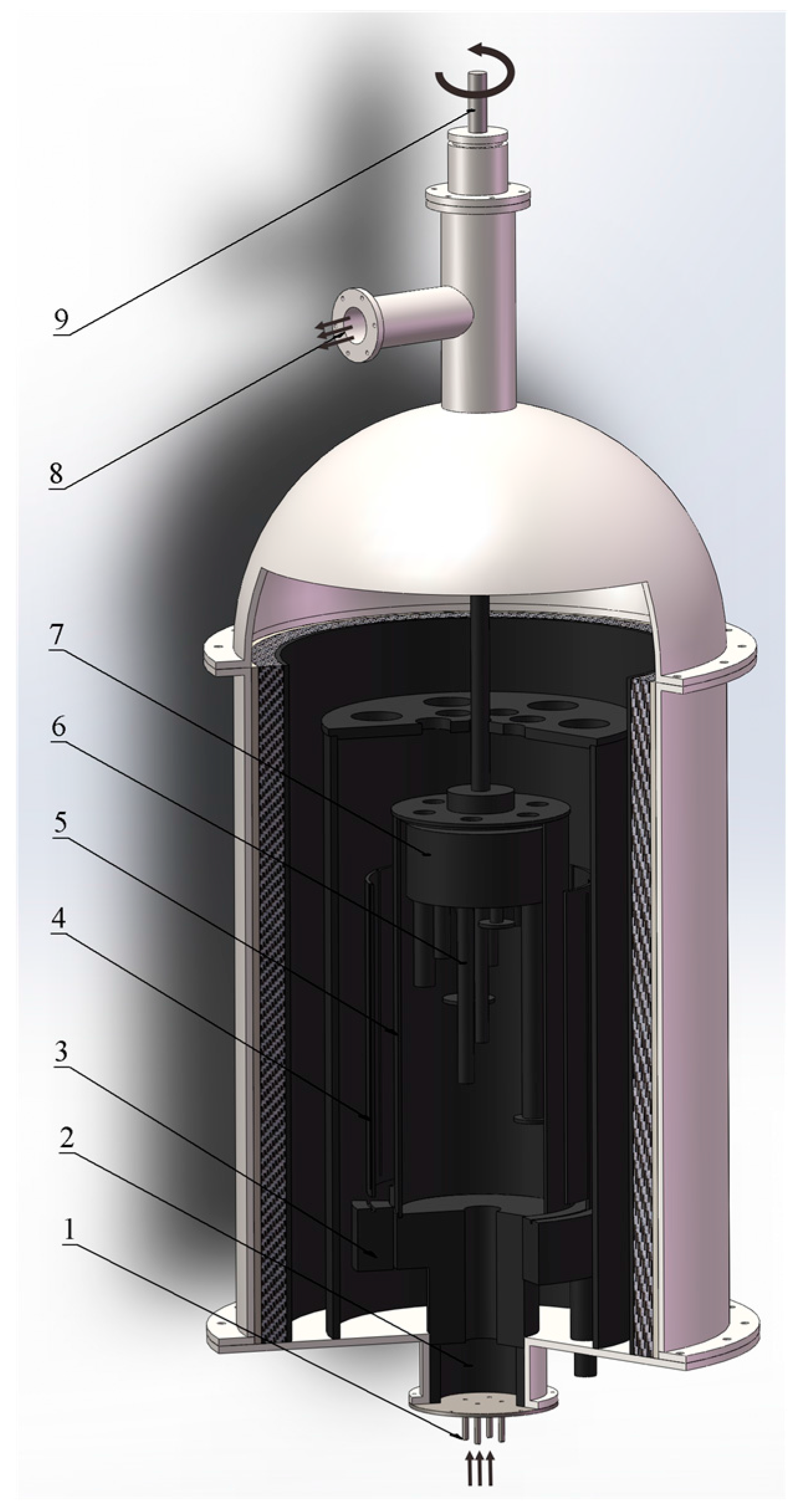
The 3D model diagram of the CVD reactor is illustrated in Figure 1. BCl3, TiCl4, and H2 enter the deposition chamber through the air inlet at the bottom of the CVD reactor, however, H2, BCl3, and TiCl4 were mixed in the gas mixing chamber before importing the deposition chamber. The graphite substrates were fixed on the sample stage. When the reaction begins, the rotating shaft drives the sample table to drive the graphite substrate to rotate. The rotating graphite substrate ensures the uniform films. A vacuum pump is connected to the air outlet for the aim of keeping the reactor in a vacuum during this entire sequence. The vacuum level was maintained at about 10 Pa during the reaction. During experimentation, TiCl4 and BCl3 were carried to the reactor by a heated line. The temperature of the TiCl4 flow was 135 °C, and the BCl3 flow was 12 °C. The heated TiCl4 flow and BCl3 flow were controlled by a mass flowmeter. Table 1 summarizes the field of deposition parameters.
In this study, the deposition was carried out at 1000 °C. The deposition pressure was 10 Pa, and the deposition time was 3 h. In the experiment, the supply of hydrogen was excessive, and the BCl3 flow rate was kept at 0.085 m3/h, then two types of specimens were synthesized at two TiCl4 flow rate levels: 0.055 m3/h and 0.11 m3/h. When the TiCl4 flow rate was 0.055 m3/h, the gas flow ratio of TiCl4/BCl3 (κ) was 0.5. At this point, κ was the stoichiometric TiCl4/BCl3 gas ratio. When the TiCl4 flow rate was 0.11 m3/h, κ was 1. TiCl4 was excessive in this situation. The microstructure and properties of these two types of films were investigated. In this way, the influence of the TiCl4/BCl3 gas flow ratio on the grain size and the deposition rate was studied.
The crystal phase of the films was determined by XRD (X’Pert Pro, PANalytical B.V., Almelo, The Netherlands). Special emphasis was put on the comparative analysis of micro structural characterization of these two types of films. In addition, SEM (Ultra Plus, ZEISS, Heidenheim, Germany), TEM (Tecnai G2 20, FEI, Hillsboro, OR, USA), and EDS (X-Max 50, OXFORD, Oxford, UK) were employed.
3. Results and Discussion
3.1. Structure, Morphology, and the Deposition Rate of Films
It was found that the oriented growth was related to the ratio of TiCl4/BCl3 from the orientation characteristics of the deposited layers investigated by X-ray diffraction shown in Figure 2 for a laser power 3 kW and laser scanning speed 2.5 mm/s. Figure 2a,b show the diffraction patterns of the deposits, which were prepared at κ = 0.5 and 1, respectively. In addition, the TiB2 standard data from the Joint Committee on Powder Diffraction Standards (JCPDS) is shown in Figure 2c. X-ray diffraction (Figure 2a,b) indicated the presence of only TiB2, with no unidentified peaks. Figure 2 also shows that the diffraction pattern of deposits corresponds well to the JCPDS standard for TiB2. Furthermore, we found that the pattern intensity of the TiB2 films, which were deposited at different gas ratios of TiCl4/BCl3 (Figure 2a,b), follows a similar trend. The intensity of the (100) peaks in Figure 2a,b are the highest of all peaks, respectively. However, there is an enhanced intensity at the (100) peaks compared with the standard pattern intensity shown in the JCPDS card NO. 85-2083 (Figure 2c). Furthermore, according the XRD analysis, the relative intensity value of R(100)/(101) is1.32 ± 0.01 (Figure 2a) and 1.28 ± 0.01 (Figure 2b). Similarly, the relative intensity of the standard pattern yields a R(100)/(101) value of 0.86 ± 0.01 (Figure 2c). Obviously, the R(100)/(101) values of the as-prepared TiB2 films are greater than the standard values. Hence, all the as-prepared TiB2 films have a preferred orientation along the (100) planes. These results are consistent with the work done by S.H. Lee [11], who reported that the film structure has a (100) preferred orientation when the film was deposited at a low RF power (200 W). The difference is that they prepared the TiB2 film at a low temperature (250~400 °C) using a PACVD system.
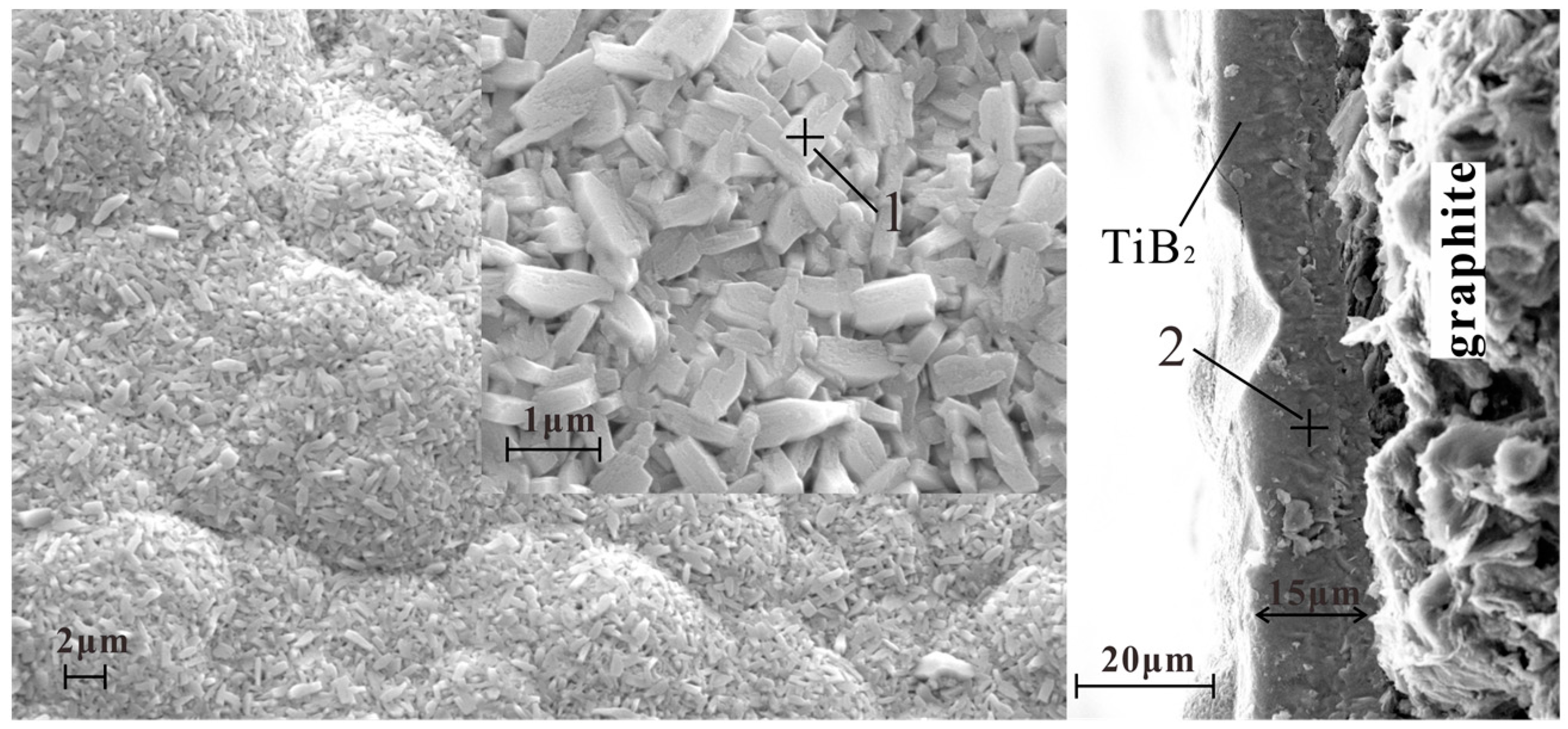
The surfaces and cross sections of the TiB2 films obtained by κ 0.5 and 1 were observed by FESEM (Figure 3 and Figure 4, respectively) with high voltages of 15 kV and magnifications of 5000× and 20,000×. EDS results are also shown. An unsmooth surface can be observed on the films. The cross sections show a very compact and dense structure without any gaps. Figure 4 indicates the FESEM images and EDS results of the surface and cross section of TiB2 films formed under the conditions of κ = 1. It can be discussed on different micrographs of the surfaces and cross sections by Figure 3 and Figure 4. It was found that similar morphologies of the TiB2 films were obtained by different gas flow ratios of TiCl4/BCl3. All TiB2 films were found to have a typically columnar particle structure, and the columnar particles have a random orientation. This indicates that there was no distinct effect on morphologies by the TiCl4/BCl3 gas flow ratio in this experimentation. However, different film thicknesses were displayed in the cross sections (Figure 3 and Figure 4). As shown in Figure 3, the thickness of the film deposited at κ = 0.5 for 3 h reached 15 microns. The thickness was 21 microns when κ was equal to 1 in Figure 4. Obviously, a thicker TiB2 film was obtained by a greater TiCl4/BCl3 gas flow ratio that goes beyond the stoichiometric TiCl4/BCl3 gas flow ratio. In other words, the film deposited faster when TiCl4 was excessive.
Table 2 shows the compositional analysis results of Spot 1, Spot 2, Spot 3, and Spot 4, analyzed via EDS. The Ti/B ratio of the deposit approached the stoichiometric value of 0.5 when the gas flow ratio of TiCl4/BCl3 was increased. According to the CVD phase diagram of the Ti–B–H–Cl system which was calculated by Randich and Gerlach [23], the formability of TiB2 relies on the distance between the process tie line and the phase boundary of the TiB2+ gas and the gas phases. A boron rich TiBx film was deposited when the BCl3 concentration was high, because the process tie line went through the region of the B + TiB2 + gas phase. Therefore, at a low TiCl4/BCl3 gas ratio, boron rich TiBx films were formed instead of TiB2.
3.2. Grain Size of the Films
Many scholars [6,11,19] have researched the influence of deposition temperature on grain size, and they all agreed that the grain size increases with increasing temperature. Indeed, this conclusion is in good agreement with the kinetic theory of CVD [24]. Comparatively few research groups have studied the effect of TiCl4/BCl3 gas flow ratio on grain size.
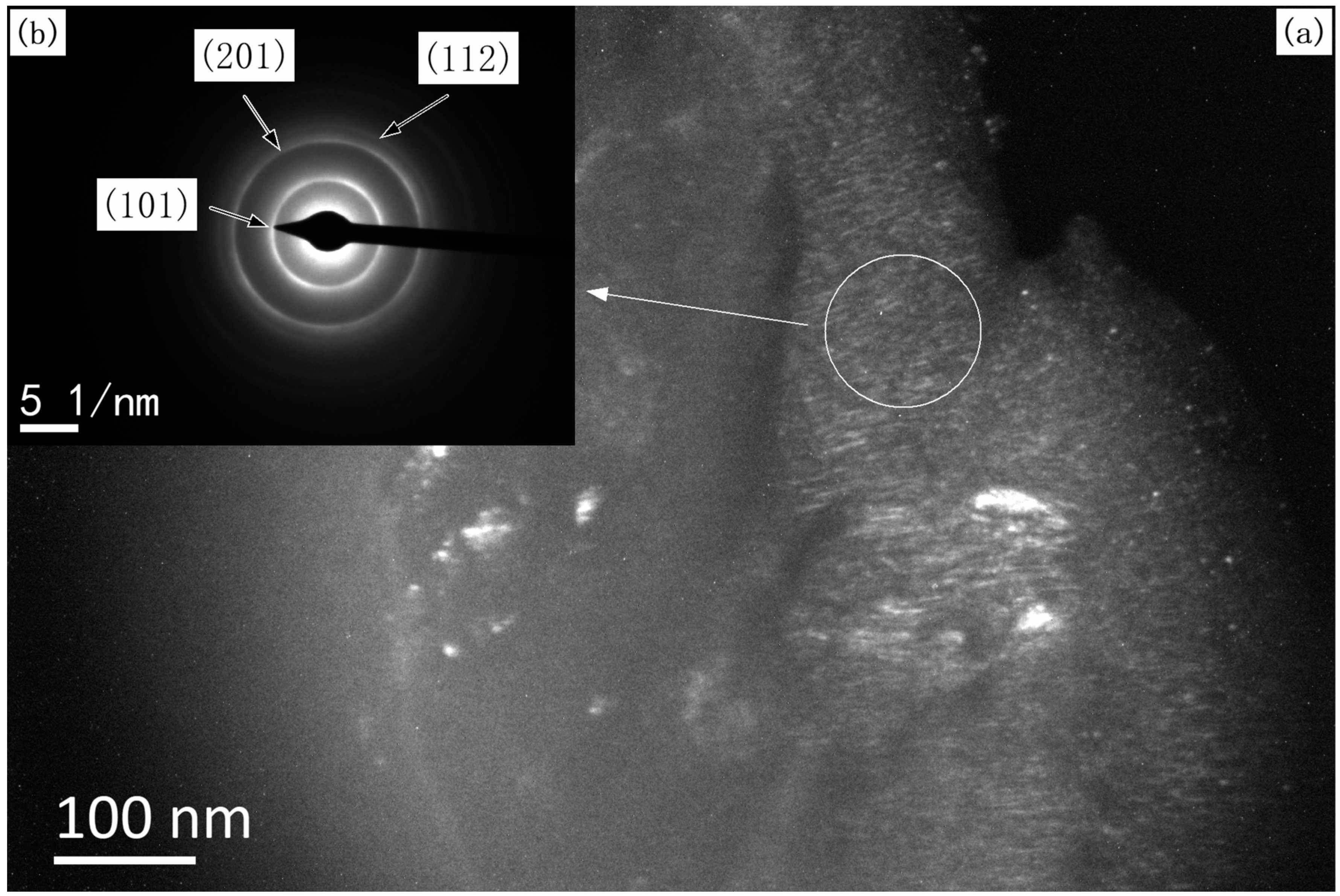
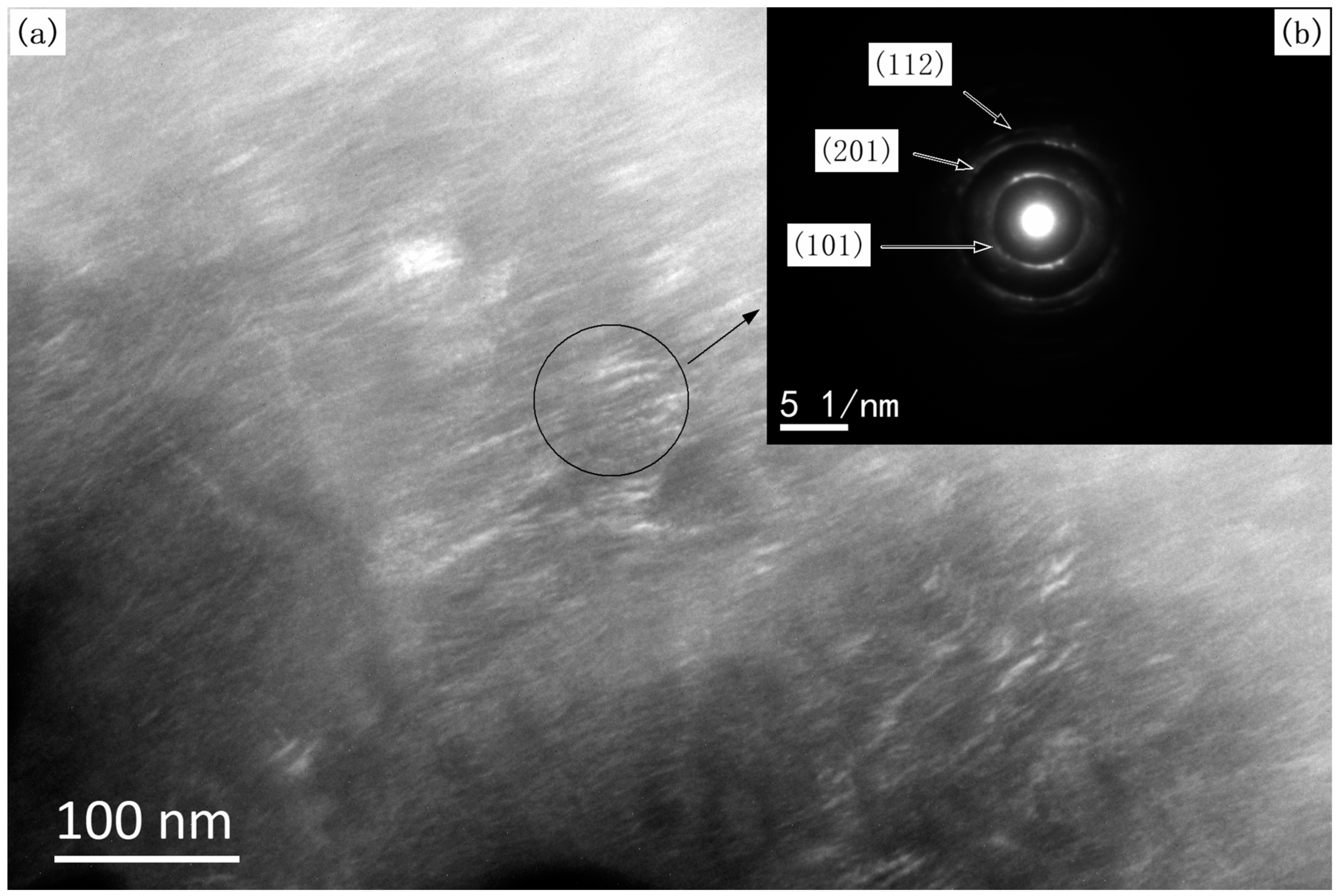
The grain size of the TiB2 films was calculated by XRD patterns of TiB2 films (Figure 2) using the Scherrer formula. The grain size was 58 ± 3 nm when the TiB2 film was deposited at a stoichiometric TiCl4/BCl3 gas ratio of 0.5, and the grain size was 69 ± 3 nm when κ = 1. Hence, all the as-deposited TiB2 films had a nano-sized grain structure. Figure 5 and Figure 6 show TEM images of the films formed under different gas flow ratios of TiCl4/BCl3. Bright nano-sized shapes can be observed in the dark field images (Figure 5a and Figure 6a), wherein it can be seen that the common shapes of the grains reveal a columnar and that the grain size is at the nano scale. The grain size is also easily observed. The grains are larger in Figure 6a than in Figure 5a. Analysis of the selected-area electron diffraction (SAED) pattern (Figure 5b and Figure 6b) revealed only the presence of TiB2. The average grain size in the plan view (dark field image) was estimated to be at the nano scale and to cause continuous rings in the diffraction pattern (as shown in Figure 5b and Figure 6b). However, the diffraction ring, as shown in Figure 5b and Figure 6b, is a little bit different. In Figure 5b, the diffraction ring is smooth and continuous. In contrast, the ring intensities in Figure 6b do not show uniform continuity, and there are bright spots on the circular rings. This is because the grain of the selected area in Figure 6a is larger. Thus, the SAED pattern further reveals that the grain size in Figure 6a is greater than that in Figure 5a. These SAED results correspond to Figure 5a and Figure 6a. As a result, TEM investigations indicate that all as-prepared TiB2 films are nanocrystalline and that the grain size is different under various TiCl4/BCl3 gas flow ratios. Obviously, the TEM results are in good agreement with the results calculated by the Scherrer formula. Therefore, TiCl4/BCl3 gas flow ratio has a certain impact on the grain size of as-prepared TiB2 films via CVD. The grain size of TiB2 films deposited at κ = 1 is greater than that of other films obtained under conditions where κ = 0.5.
4. Conclusions
TiB2 was prepared via the vapor-phase reaction of TiCl4, BCl3, and H2 on a high pure graphite substrate. The following information was obtained:
- TiB2 could be deposited at 1000 °C and 10 Pa by a CVD system. All deposits obtained under the condition of excessive hydrogen and different TiCl4/BCl3 gas flow ratios (1/2 and 1/1) were TiB2. Other impurity phases such as TiB were not found.
- These TiB2 films are nanocrystalline with a grain size in the range of 60 nm. All of the TiB2 films were typically columnar particles structure, and the columnar particles have a random orientation.
- X-ray diffraction indicated that all of the as-synthesized TiB2 films have a preferential orientation growth in the (100) direction.
- The TiCl4/BCl3 gas flow ratio has a certain impact on deposition rate and grain size, but these variations in the gas flow ratio of TiCl4/BCl3 did not appear to influence the preferred orientation of the deposits. The deposition rate is faster when using a greater TiCl4/BCl3 gas flow ratio, which in this case was 1/1. Meanwhile, when we provided a stoichiometric TiCl4/BCl3 gas ratio of 1/2, the grain size of the as-deposited TiB2 film was smaller.
Acknowledgments
The authors are grateful for the financial support of the Foundation Committee of the National Nature of China (No. 50904017). Their support enabled us to complete this work.
Author Contributions
Xiaoxiao Huang planned and performed the experiments, analyzed the experimental data, and wrote the manuscript. Shuchen Sun directed and guided the research and extensively provided help for editing the manuscript. Ganfeng Tu provided useful insights into the manuscript. Shuaidan Lu took the TEM images. Kuanhe Li and Xiaoping Zhu prepared the TEM samples. All authors contributed in discussion and preparation of the manuscript.
Conflicts of Interest
The authors declare no conflict of interest.
References
- Schalk, N.; Keckes, J.; Czettl, C.; Burghammer, M.; Penoy, M.; Michotte, C.; Mitterer, C. Investigation of the origin of compressive residual stress in CVD TiB2 hard coatings using synchrotron X-ray nanodiffraction. Surf. Coat. Technol. 2014, 258, 121–126. [Google Scholar] [CrossRef]
- Raju, G.B.; Basu, B. Development of high temperature TiB2-based ceramics. Key Eng. Mater. 2009, 395, 89–124. [Google Scholar] [CrossRef]
- Shimada, S.; Takahashi, M.; Kiyono, H.; Tsujino, J. Coatings and microstructures of monolithic TiB2 films and double layer and composite TiCN/TiB2 films from alkoxide solutions by thermal plasma CVD. Thin Solid Films 2008, 516, 6616–6621. [Google Scholar] [CrossRef]
- Tang, W.-M.; Zheng, Z.-X.; Wu, Y.-C.; Wang, J.-M.; Lü, J.; Liu, J.-W. Synthesis of TiB2 nanocrystalline powder by mechanical alloying. Trans. Nonferrous Met. Soc. China 2006, 16, 613–617. [Google Scholar] [CrossRef]
- Berger, M.; Coronel, E.; Olsson, E. Microstructure of d.c. Magnetron sputtered TiB2 coatings. Surf. Coat. Technol. 2004, 185, 240–244. [Google Scholar] [CrossRef]
- Pfohl, C.; Bulak, A.; Rie, K.T. Development of titanium diboride coatings deposited by PACVD. Surf. Coat. Technol. 2000, 131, 141–146. [Google Scholar] [CrossRef]
- Martin, C.; Cales, B.; Vivier, P.; Mathieu, P. Electrical discharge machinable ceramic composites. Mater. Sci. Eng. A 1989, 109, 351–356. [Google Scholar] [CrossRef]
- Tennery, V.; Finch, C.; Yust, C.; Clark, G. Structure-property correlations for TiB2-based ceramics densified using active liquid metals. In Science of Hard Materials; Springer: Boston, MA, USA, 1983; pp. 891–909. ISBN 978-1-4684-4319-6. [Google Scholar]
- Ferber, M.K.; Becher, P.F.; Finch, C.B. Effect of microstructure on the properties of TiB2 ceramics. J. Am. Ceram. Soc. 1983, 66, C-2–C-3. [Google Scholar] [CrossRef]
- Subramanian, C.; Murthy, T.S.R.C.; Suri, A.K. Synthesis and consolidation of titanium diboride. Int. J. Refract. Met. Hard Mater. 2007, 25, 345–350. [Google Scholar] [CrossRef]
- Lee, S.H.; Nam, K.H.; Hong, S.C.; Lee, J.J. Low temperature deposition of TiB2 by inductively coupled plasma assisted CVD. Surf. Coat. Technol. 2007, 201, 5211–5215. [Google Scholar] [CrossRef]
- Elders, J.; van Voorst, J.D.W. Laser-induced chemical vapor deposition of titanium diboride. Appl. Surf. Sci. 1992, 54, 135–140. [Google Scholar] [CrossRef]
- Sun, L.; Gao, Y.; Xiao, B.; Li, Y.; Wang, G. Anisotropic elastic and thermal properties of titanium borides by first-principles calculations. J. Alloys Compd. 2013, 579, 457–467. [Google Scholar] [CrossRef]
- Wang, H.; Sun, S.; Wang, D.; Tu, G. Characterization of the structure of TiB2/TiC composites prepared via mechanical alloying and subsequent pressureless sintering. Powder Technol. 2012, 217, 340–346. [Google Scholar] [CrossRef]
- Vallauri, D.; Atías Adrián, I.C.; Chrysanthou, A. TiC–TiB2 composites: A review of phase relationships, processing and properties. J. Eur. Ceram. Soc. 2008, 28, 1697–1713. [Google Scholar] [CrossRef]
- Jeitschko, W.; Pöttgen, R.; Hoffman, R. Structural chemistry of hard materials. In Handbook of Ceramic Hard Materials, 1st ed.; Wiley-VCH: New York, NY, USA, 2008; pp. 10–11. ISBN 9783527618217. [Google Scholar]
- Batanov, G.M.; Berezhetskaya, N.K.; Borzosekov, V.D.; Iskhakova, L.D.; Kolik, L.V.; Konchekov, E.M.; Letunov, A.A.; Malakhov, D.V.; Milovich, F.O.; Obraztsova, E.A.; et al. Application of microwave discharge for the synthesis of TiB2 and bn nano- and microcrystals in a mixture of Ti-B powders in a nitrogen atmosphere. Plasma Phys. Rep. 2013, 39, 843–848. [Google Scholar] [CrossRef]
- Kang, S.H.; Kim, D.J. Synthesis of nano-titanium diboride powders by carbothermal reduction. J. Eur. Ceram. Soc. 2007, 27, 715–718. [Google Scholar] [CrossRef]
- Caputo, A.J. Chemical vapor deposition of erosion-resistant TiB2 coatings. J. Electrochem. Soc. 1985, 132. [Google Scholar] [CrossRef]
- Pierson, H.O.; Randich, E.; Mattox, D.M. The chemical vapor deposition of TiB2 on graphite. J. Less Common Met. 1979, 67, 381–388. [Google Scholar] [CrossRef]
- Takahashi, T.; Kamiya, H. Chemical vapor deposition of titanium diboride. J. Cryst. Growth 1974, 26, 203–209. [Google Scholar] [CrossRef]
- Williams, L.M. Plasma enhanced chemical vapor deposition of titanium diboride films. Appl. Phys. Lett. 1985, 46, 43–45. [Google Scholar] [CrossRef]
- Randich, E.; Gerlach, T.M. The calculation and use of chemical vapor deposition phase diagrams with applications to the Ti–B–Cl–H system between 1200 and 800 K. Thin Solid Films 1981, 75, 271–291. [Google Scholar] [CrossRef]
- Pierson, H.O. Fundamentals of Chemical Vapor Deposition. In Handbook of Chemical Vapor Deposition: Principles, Technology and Applications, 2nd ed.; William Andrew: New York, NY, USA, 1999; pp. 43–63. ISBN 0815517432. [Google Scholar]
Figure 1.
3D model diagram of the CVD (chemical vapor deposition) reactor. (1) Air inlet; (2) gas mixing chamber; (3) electrode; (4) heating resistor; (5) deposition chamber; (6) high purity graphite substrate; (7) sample stage; (8) air outlet; (9) rotating shaft.
Figure 1.
3D model diagram of the CVD (chemical vapor deposition) reactor. (1) Air inlet; (2) gas mixing chamber; (3) electrode; (4) heating resistor; (5) deposition chamber; (6) high purity graphite substrate; (7) sample stage; (8) air outlet; (9) rotating shaft.

Figure 2.
XRD (X-ray diffraction) patterns of TiB2 deposits. (a) At a gas flow ratio of TiCl4/BCl3 = 0.5; (b) at a gas flow ratio of TiCl4/BCl3 = 1; (c) TiB2 standard data from JCPDS (Joint Committee on Powder Diffraction Standards) card No. 85-2083.
Figure 2.
XRD (X-ray diffraction) patterns of TiB2 deposits. (a) At a gas flow ratio of TiCl4/BCl3 = 0.5; (b) at a gas flow ratio of TiCl4/BCl3 = 1; (c) TiB2 standard data from JCPDS (Joint Committee on Powder Diffraction Standards) card No. 85-2083.
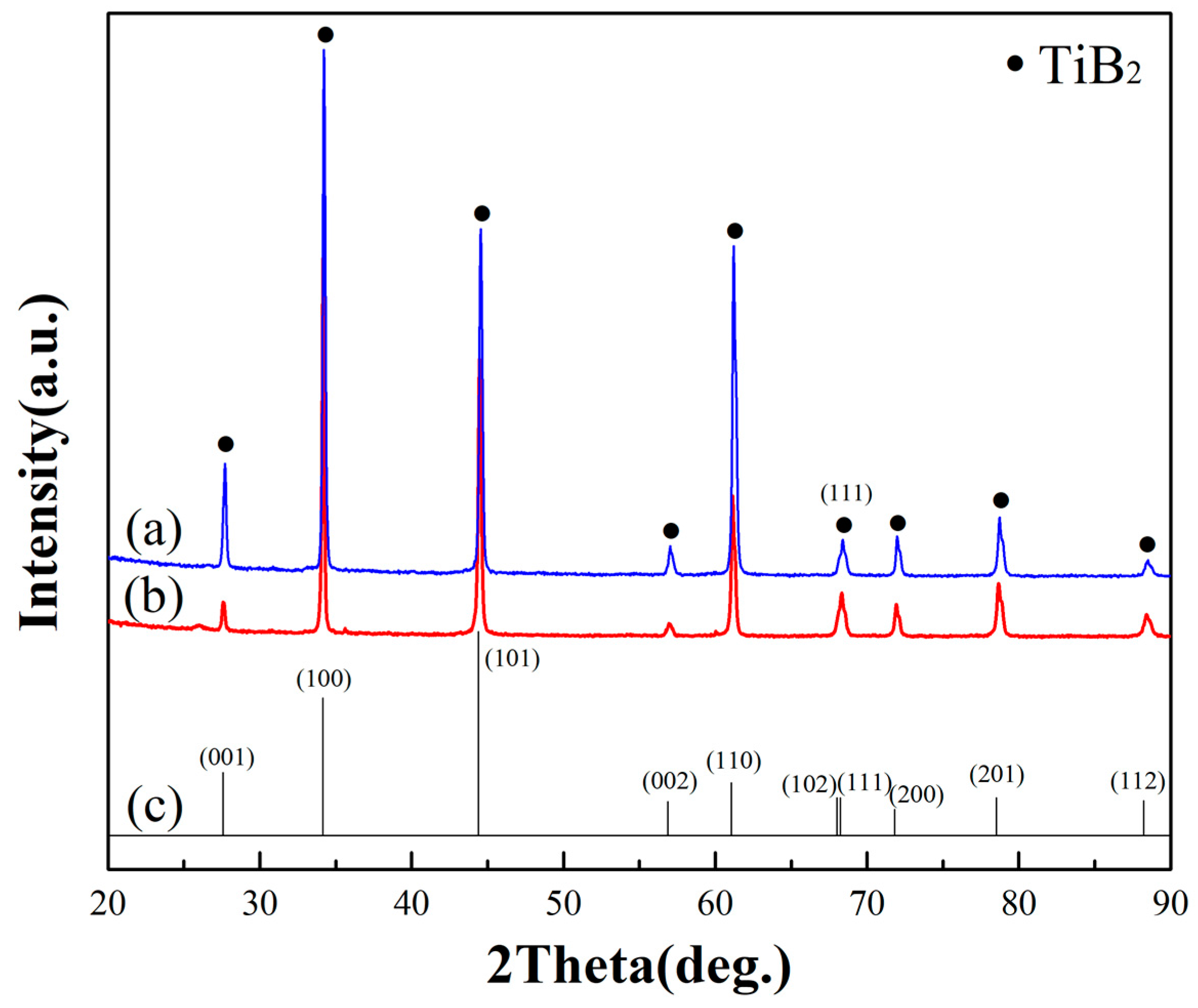
Figure 3.
SEM (scanning electron microscopy) images and EDS (energy dispersive spectroscopy) results of the surface and cross section of the TiB2 film formed under the condition of a TiCl4/BCl3 gas flow ratio of 0.5.
Figure 3.
SEM (scanning electron microscopy) images and EDS (energy dispersive spectroscopy) results of the surface and cross section of the TiB2 film formed under the condition of a TiCl4/BCl3 gas flow ratio of 0.5.

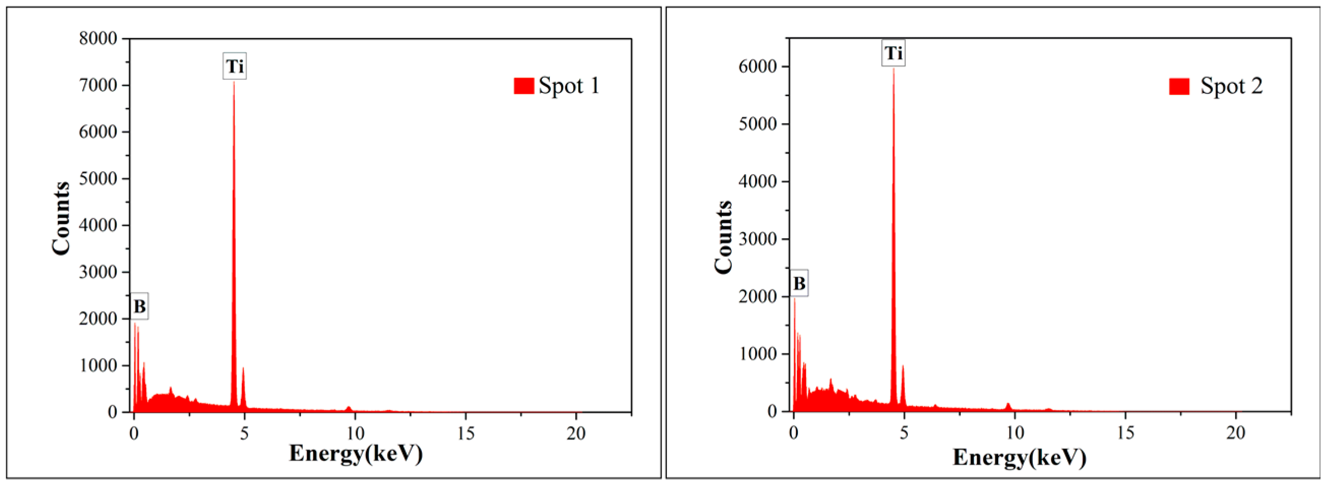
Figure 4.
SEM images and EDS results of the surface and cross section of the TiB2 film formed under the condition of a TiCl4/BCl3 gas flow ratio of 1.
Figure 4.
SEM images and EDS results of the surface and cross section of the TiB2 film formed under the condition of a TiCl4/BCl3 gas flow ratio of 1.
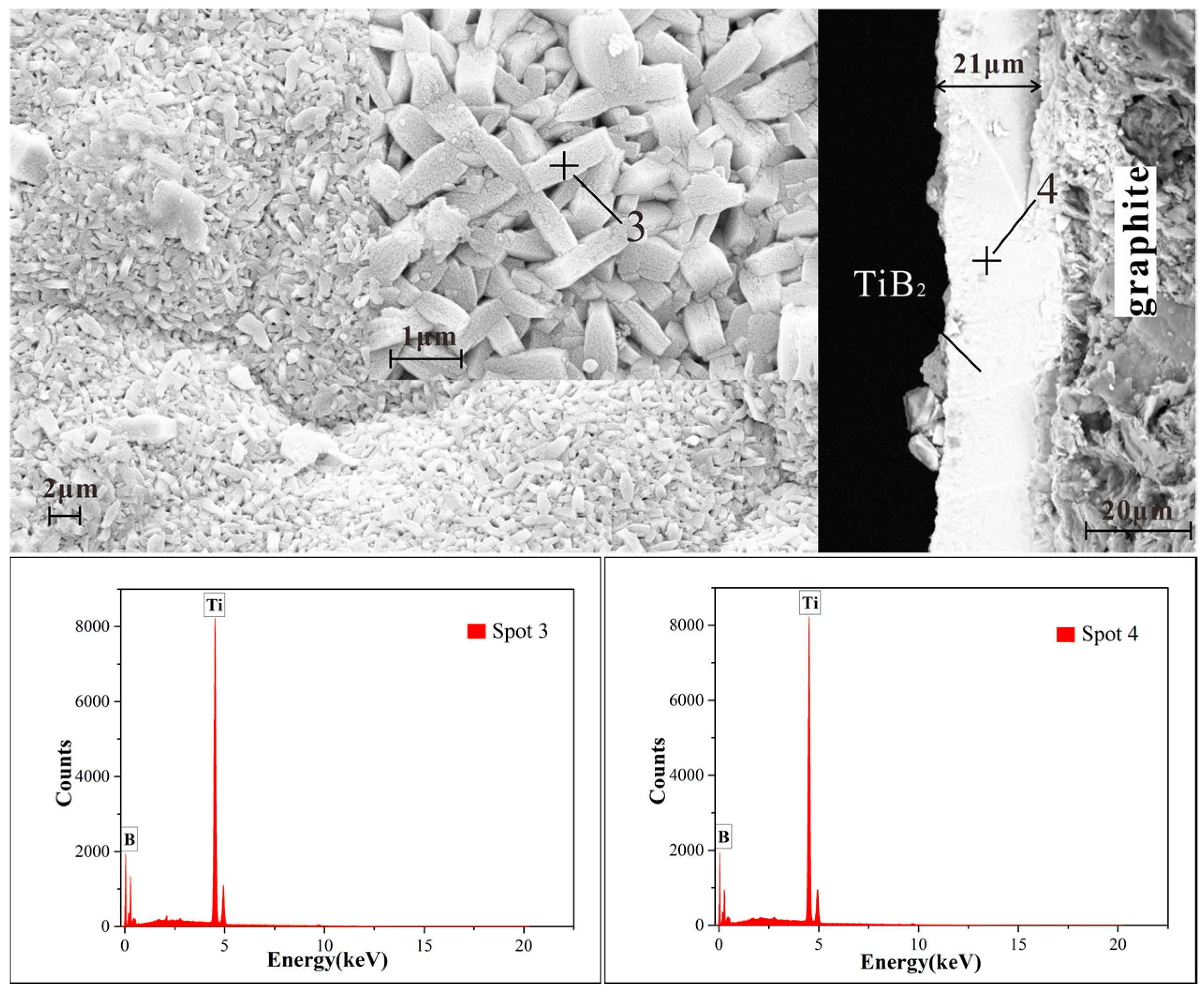
Figure 5.
TEM images of the synthesized TiB2 film formed by CVD with a TiCl4/BCl3 gas flow ratio of 0.5: (a) dark field image, (b) corresponding selected-area electron diffraction pattern.
Figure 5.
TEM images of the synthesized TiB2 film formed by CVD with a TiCl4/BCl3 gas flow ratio of 0.5: (a) dark field image, (b) corresponding selected-area electron diffraction pattern.

Figure 6.
TEM images of the synthesized TiB2 film formed by CVD with a TiCl4/BCl3 gas flow ratio of 1: (a) dark field image, (b) corresponding selected-area electron diffraction pattern.
Figure 6.
TEM images of the synthesized TiB2 film formed by CVD with a TiCl4/BCl3 gas flow ratio of 1: (a) dark field image, (b) corresponding selected-area electron diffraction pattern.


Table 1.
Field of deposition parameters.
| Substrate | Graphite |
|---|---|
| deposition temperature | 1000 (°C) |
| deposition time | 3 (h) |
| vacuum level | 10 (Pa) |
| temperature of H2 | 25 (°C) |
| pressure of H2 | 0.06 (MPa) |
| flow rate of H2 | 0.9 (m3/h) |
| temperature of TiCl4 | 135 (°C) |
| pressure of TiCl4 | 0.1 (MPa) |
| flow rate of TiCl4 | 0.055, 0.11 (m3/h) |
| temperature of BCl3 | 12 (°C) |
| pressure of BCl3 | 0.1 (MPa) |
| flow rate of BCl3 | 0.085 (m3/h) |
© 2017 by the authors. Licensee MDPI, Basel, Switzerland. This article is an open access article distributed under the terms and conditions of the Creative Commons Attribution (CC BY) license (http://creativecommons.org/licenses/by/4.0/).
Share and Cite
MDPI and ACS Style
Huang, X.; Sun, S.; Tu, G.; Lu, S.; Li, K.; Zhu, X. The Microstructure of Nanocrystalline TiB2 Films Prepared by Chemical Vapor Deposition. Materials 2017, 10, 1425. https://doi.org/10.3390/ma10121425
AMA Style
Huang X, Sun S, Tu G, Lu S, Li K, Zhu X. The Microstructure of Nanocrystalline TiB2 Films Prepared by Chemical Vapor Deposition. Materials. 2017; 10(12):1425. https://doi.org/10.3390/ma10121425
Chicago/Turabian StyleHuang, Xiaoxiao, Shuchen Sun, Ganfeng Tu, Shuaidan Lu, Kuanhe Li, and Xiaoping Zhu. 2017. "The Microstructure of Nanocrystalline TiB2 Films Prepared by Chemical Vapor Deposition" Materials 10, no. 12: 1425. https://doi.org/10.3390/ma10121425
Note that from the first issue of 2016, this journal uses article numbers instead of page numbers. See further details here.