Phosphor-Free InGaN White Light Emitting Diodes Using Flip-Chip Technology

 , ,
, ,
Abstract
:
1. Introduction
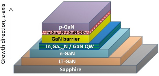
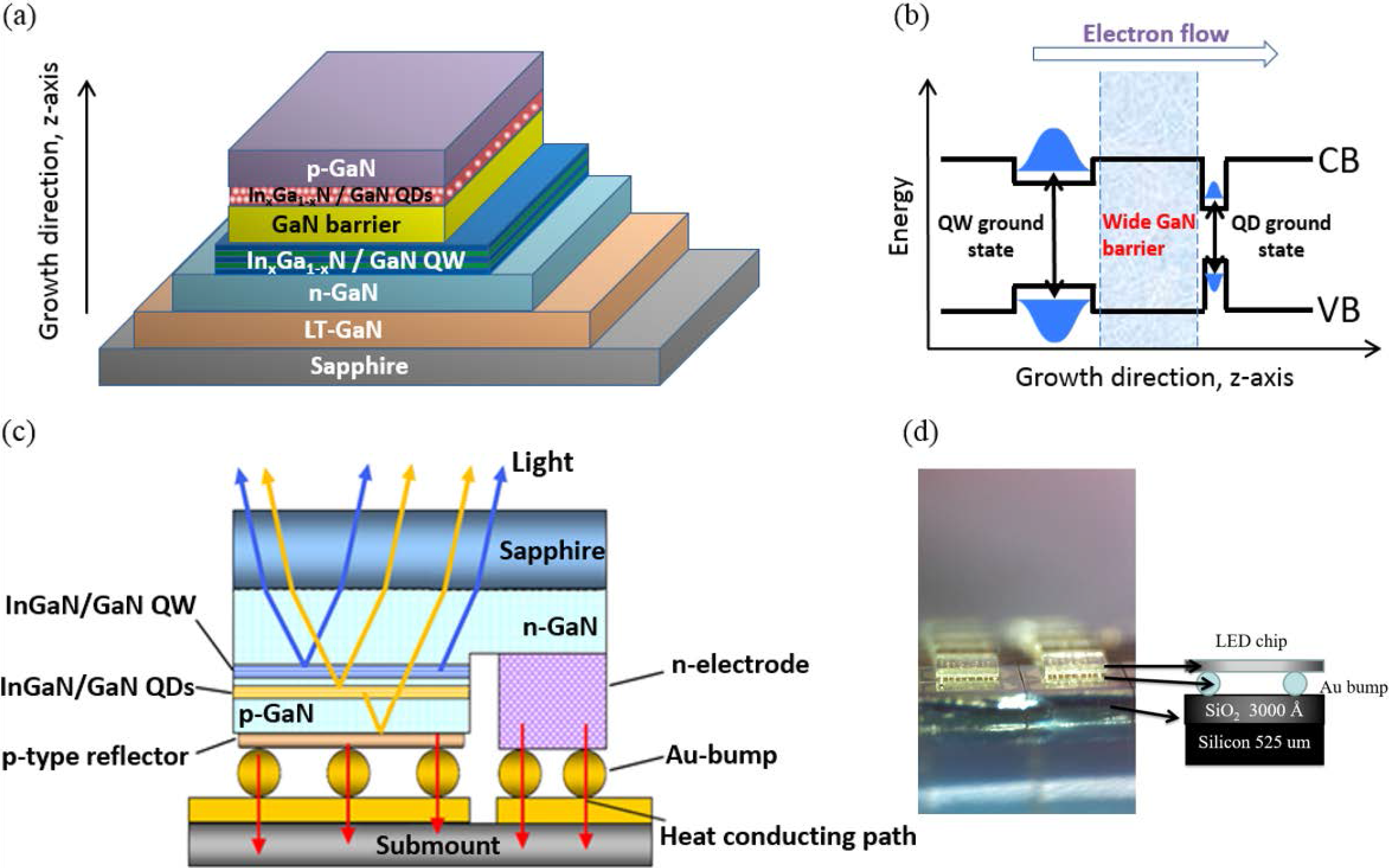
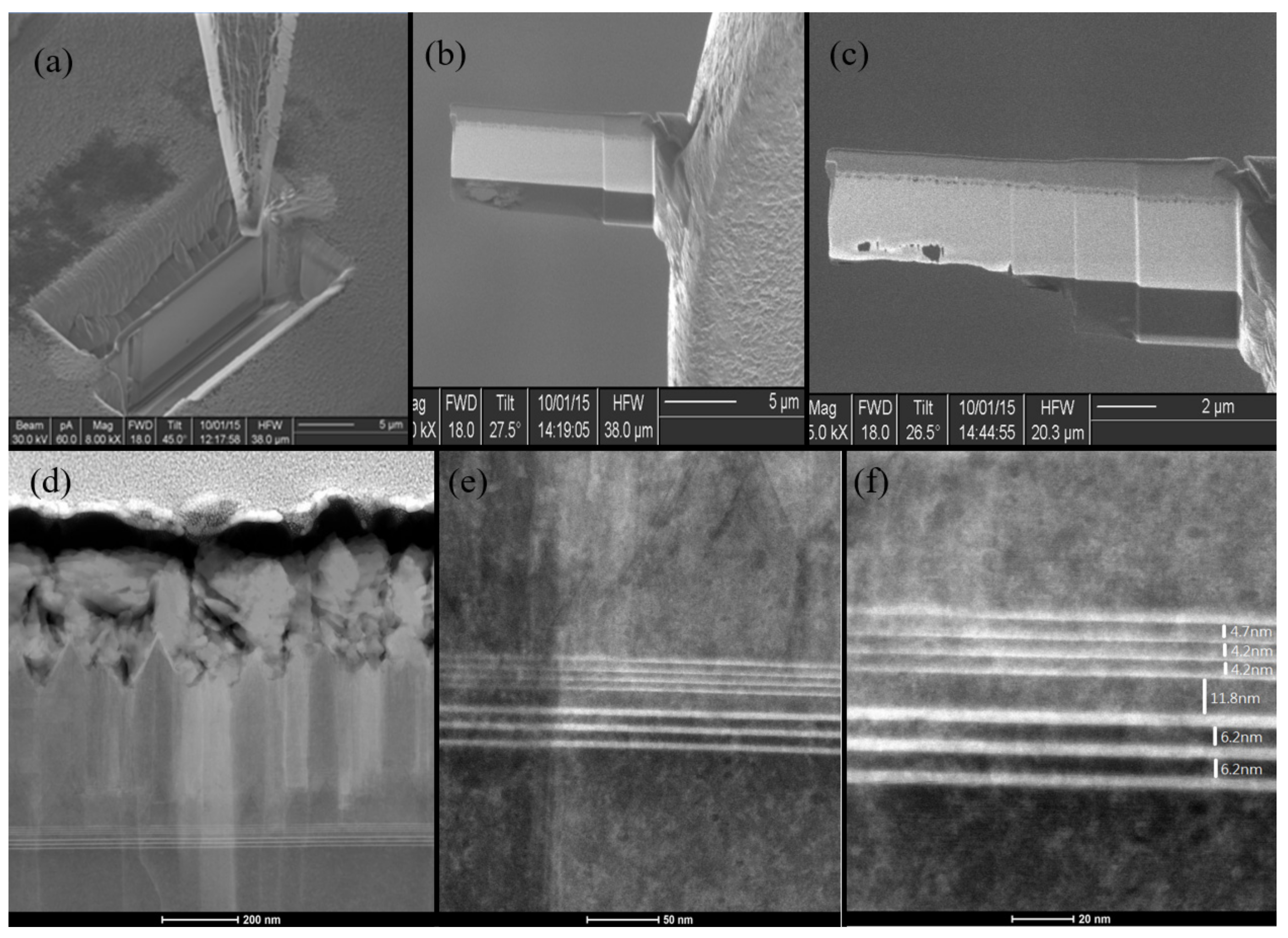
2. Experiments
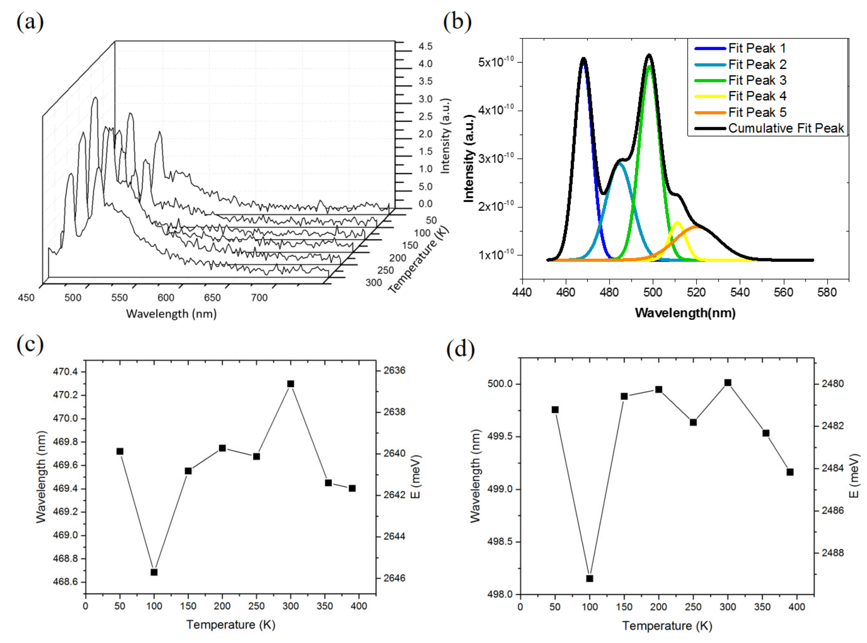
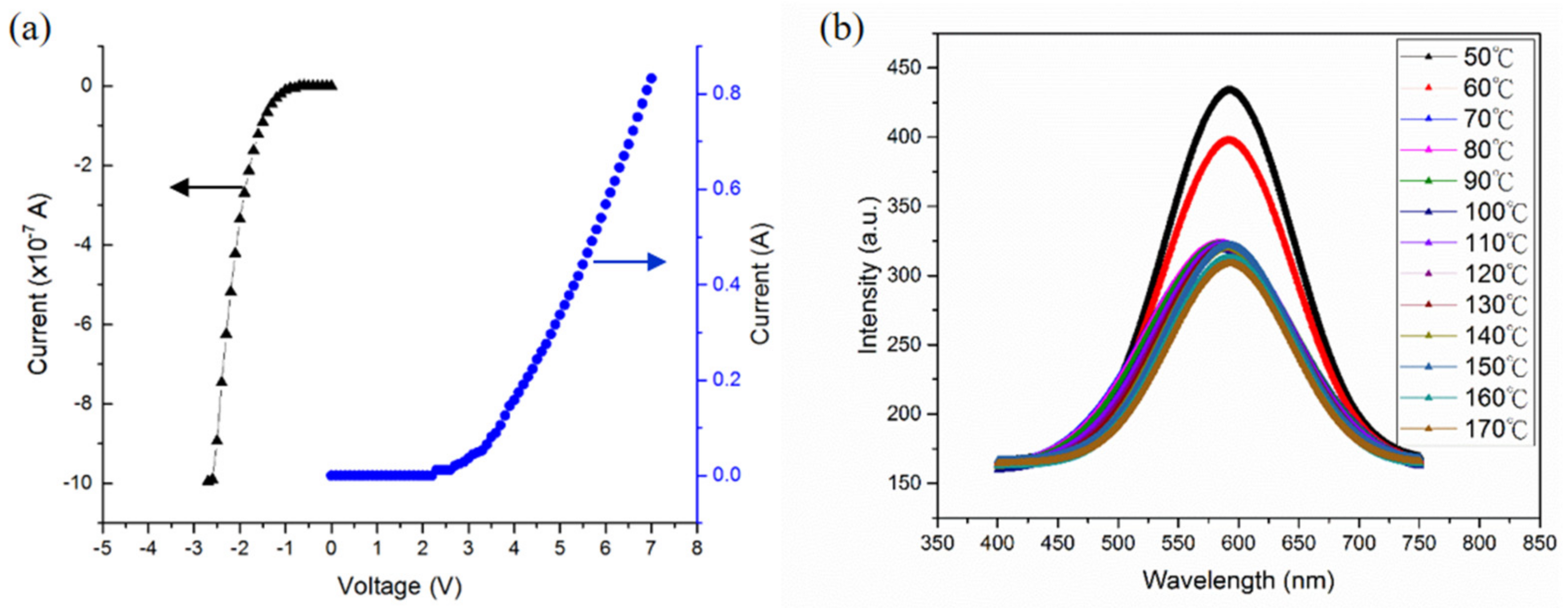
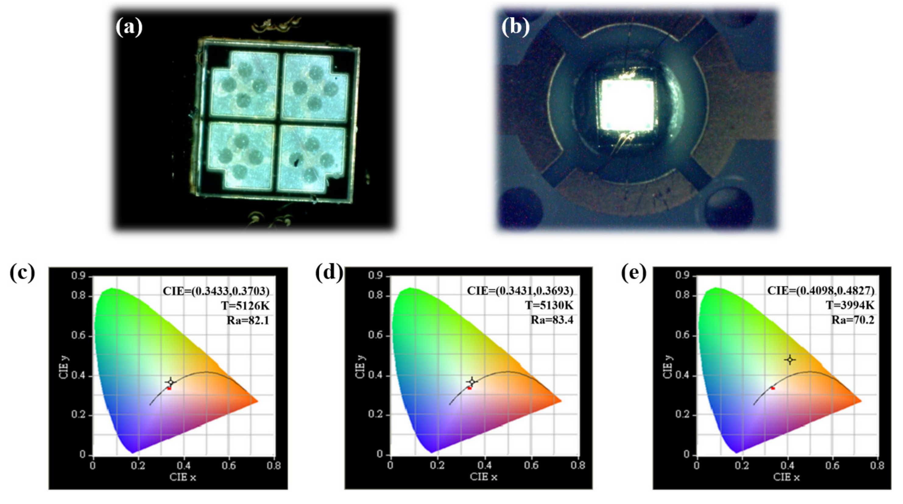
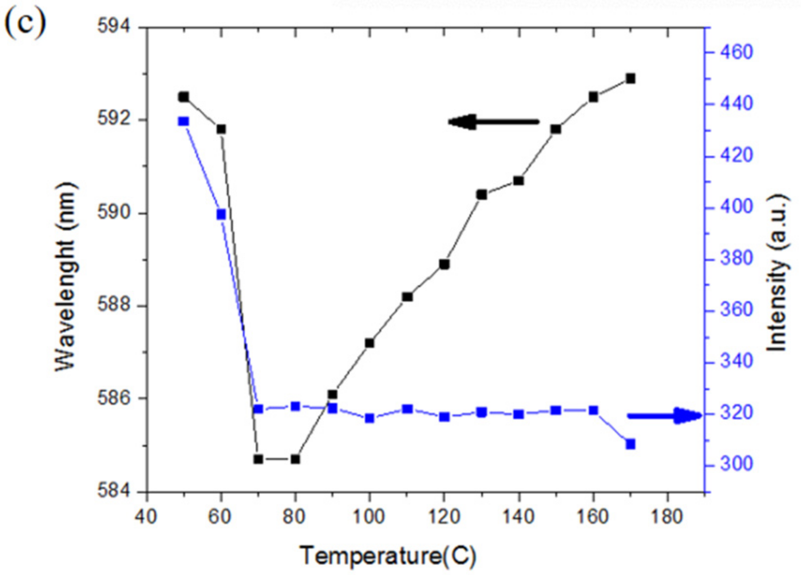
3. Results and Discussion
3.1. Characterizations of the QD/QW Structure
3.2. Device Characterization of QD/QW LEDs
3.3. Light Mixing Properties
4. Conclusions
Acknowledgments
Author Contributions
Conflicts of Interest
Appendix A

| Bias Current | 350 mA | 500 mA | 700 mA |
|---|---|---|---|
| R1 | 92.41866 | 88.78911 | 60.93052 |
| R2 | 92.13289 | 95.05205 | 71.70682 |
| R3 | 77.45595 | 79.1353 | 87.9434 |
| R4 | 71.69764 | 73.43228 | 66.92189 |
| R5 | 88.66449 | 87.51749 | 61.88037 |
| R6 | 90.6693 | 94.98337 | 65.34932 |
| R7 | 75.32654 | 78.32166 | 91.69814 |
| R8 | 69.06432 | 70.10013 | 55.46916 |
| R9 | 43.20995 | 40.38482 | −35.15676 |
| R10 | 81.89597 | 87.42805 | 40.71531 |
| R11 | 75.54762 | 77.11202 | 56.45898 |
| R12 | 77.31905 | 74.24747 | 43.0356 |
| R13 | 95.75813 | 93.01258 | 61.30183 |
| R14 | 87.0627 | 87.52311 | 94.5731 |
| Ra | 82.17872 | 83.41642 | 70.23745 |
References
- Mohammad, S.N.; Salvador, A.A.; Morkoc, H. Emerging Gallium Nitride Based Devices. Proc. IEEE 1995, 83, 1306–1355. [Google Scholar] [CrossRef]
- Nakamura, S.; Senoh, M.; Nagahama, S.I.; Iwasa, N.; Yamada, T.; Matsushita, T.; Kiyoku, H.; Sugimoto, Y.; Kozaki, T.; Umemoto, H.; et al. InGaN/GaN/AlGaN-Based Laser Diodes with Modulation-Doped Strained-Layer Superlattices Grown on an Epitaxially Laterally Overgrown GaN Substrate. Appl. Phys. Lett. 1998, 72, 211–213. [Google Scholar] [CrossRef]
- Muthu, S.; Gaines, J. Red, Green and Blue LED-Based White Light Source: Implementation Challenges and Control Design. In Proceedings of the 38th IAS Annual Meeting: Crossroads to Innovation, 2003 IEEE Industry Applications Conference, Salt Lake City, UT, USA, 12–16 October 2003; pp. 515–522. [Google Scholar]
- Chang, L.B.; Chang, Y.H.; Jeng, M.J. Light Output Improvement of InGaN-based light-Emitting Diodes by Microchannel Structure. IEEE Photonics Technol. Lett. 2007, 19, 1175–1177. [Google Scholar] [CrossRef]
- Lai, M.J.; Jeng, M.J.; Chang, L.B. High-Efficiency InGaN-Based Yellow-Green Light-Emitting Diodes. Jpn. J. Appl. Phys. 2010, 49, 021004. [Google Scholar] [CrossRef]
- Brinkley, S.E.; Pfaff, N.; Denault, K.A.; Zhang, Z.; Hintzen, H.T.; Seshadri, R.; Nakamura, S.; DenBaars, S.P. Robust Thermal Performance of Sr2Si5N8:Eu2+: An efficient red emitting phosphor for light emitting diode based white lighting. Appl. Phys. Lett. 2011, 99, 241106. [Google Scholar] [CrossRef]
- Oh, J.H.; Oh, J.R.; Park, H.K.; Sung, Y.-G.; Do, Y.R. Highly-Efficient, Tunable Green, Phosphor-Converted LEDs Using a Long-Pass Dichroic Filter and a Series of Orthosilicate Phosphors for Tri-Color White LEDs. Opt. Express 2011, 19, 4188–4198. [Google Scholar] [CrossRef] [PubMed]
- Setlur, A.A.; Radkov, E.V.; Henderson, C.S.; Her, J.-H.; Srivastava, A.M.; Karkada, N.; Kishore, M.S.; Kumar, N.P.; Aesram, D.; Deshpande, A.; et al. Energy-Efficient, High-Color-Rendering LED Lamps Using Oxyfluoride and Fluoride Phosphors. Chem. Mater. 2010, 22, 4076–4082. [Google Scholar] [CrossRef]
- Kuo, T.-W.; Liu, W.-R.; Chen, T.-M. High Color Rendering White Light-Emitting-Diode Illuminator Using the Red-Emitting Eu2+-Activated CaZnOS Phosphors Excited by Blue LED Available. Opt. Express 2010, 18, 8187–8192. [Google Scholar] [CrossRef] [PubMed]
- Damilano, B.; Grandjean, N.; Pernot, C.; Massies, J. Monolithic White Light Emitting Diodes Based on InGaN/GaN Multiple-Quantum Wells. Jpn. J. Appl. Phys. 2007, 40, L918–L920. [Google Scholar] [CrossRef]
- Huang, C.-F.; Lu, C.-F.; Tang, T.-Y.; Huang, J.J.; Yang, C.C. Phosphor-Free White-Light Light-Emitting Diode of Weakly Carrier-Density-Dependent Spectrum with Prestrained Growth of InGaN/GaNInGaN/GaN Quantum wells. Appl. Phys. Lett. 2007, 90, 122–151. [Google Scholar] [CrossRef]
- Liu, L.; Wang, L.; Liu, N.; Yang, W.; Li, D.; Chen, W.; Feng, Z.C.; Lee, Y.-C.; Ferguson, I.; Hu, X. Investigation of the Light Emission Properties and Carrier Dynamics in Dual-Wavelength InGaN/GaN Multiple-Quantum Well Light Emitting Diodes. J. Appl. Phys. 2012, 112, 083101. [Google Scholar] [CrossRef]
- Chi, K.-L.; Yeh, S.-T.; Yeh, Y.-H.; Lin, K.-Y.; Shi, J.-W.; Wu, Y.-R.; Lee, M.L.; Sheu, J.-K. GaN-Based Dual-Color LEDs with p-Type Insertion Layer for Controlling the Ratio of Two-Color Intensities. IEEE Trans. Electron. Devices 2013, 60, 2821–2826. [Google Scholar] [CrossRef]
- Nguyen, H.P.T.; Zhang, S.; Connie, A.T.; Kibria, M.G.; Wang, Q.; Shih, I.; Mi, Z. Breaking the Carrier Injection Bottleneck of Phosphor-Free Nanowire White Light-Emitting Diodes. Nano Lett. 2013, 13, 5437–5442. [Google Scholar] [CrossRef] [PubMed]
- Sadaf, S.M.; Ra, Y.H.; Szkopek, T.; Mi, Z. Monolithically Integrated Metal/Semiconductor Tunnel Junction Nanowire Light-Emitting Diodes. Nano Lett. 2016, 16, 1076–1080. [Google Scholar] [CrossRef] [PubMed]
- Sadaf, S.M.; Ra, Y.-H.; Nguyen, H.P.T.; Djavid, M.; Mi, Z. Alternating-Current InGaN/GaN Tunnel Junction Nanowire White-Light Emitting Diodes. Nano Lett. 2015, 15, 6696–6701. [Google Scholar] [CrossRef] [PubMed]
- Liu, M.-G.; Yang, Y.-B.; Xiang, P.; Chen, W.-J.; Han, X.-B.; Lin, X.-Q.; Lin, J.-L.; Luo, H.; Liao, Q.; Zang, W.-J. Influences of Stress on the Properties of GaN/InGaN Multiple Quantum Well LEDs Grown on Si (111) Substrates. Chin. Phys. B 2015, 24, 068503. [Google Scholar] [CrossRef]
- Lu, C.-F.; Huang, C.-F.; Chen, Y.-S.; Shiao, W.-Y.; Chen, C.-Y.; Lu, Y.-C.; Yang, C.-C. Phosphor-Free Monolithic White-Light LED. IEEE J. Sel. Top. Quantum Electron. 2009, 15, 1210–1217. [Google Scholar]
- Lai, Y.L.; Liu, C.P.; Chen, Z.Q. Study of the Dominant Luminescence Mechanism in InGaN/GaNInGaN/GaN Multiple Quantum Wells Comprised of Ultrasmall InGaN Quasiquantum Dots. Appl. Phys. Lett. 2005, 86, 121915. [Google Scholar] [CrossRef]
- Shahedipour-Sandvik, F.; Grandusky, J.R.; Jamil, M.; Jindal, V.; Schujman, S.B.; Schowalter, L.J.; Liu, R.; Ponce, F.A.; Cheung, M.; Cartwright, A. Deep Green Emission at 570 nm from InGaN/GaN MQW Active Region Grown on Bulk AlN Substrate. Proc. SPIE 2005, 5941, 594107. [Google Scholar]
- Chen, H.S.; Lu, C.F.; Yeh, D.M.; Huang, C.F.; Huang, J.J.; Yang, C.C. Orange–Red Light-Emitting Diodes Based on a Prestrained InGaN–GaN Quantum-Well Epitaxy Structure. IEEE Photonics Technol. Lett. 2006, 18, 2269. [Google Scholar] [CrossRef]
- Barletta, P.T.; Berkman, E.A.; Moody, B.F.; El-Masry, N.A.; Emara, A.M.; Reed, M.J.; Bedair, S.M. Development of Green, Yellow, and Amber Light Emitting Diodes Using InGaN Multiple Quantum Well Structures. Appl. Phys. Lett. 2007, 90, 151109. [Google Scholar] [CrossRef]
- Wu, K.; Wei, T.; Zheng, H.; Lan, D.; Wei, X.; Hu, Q.; Lu, H.; Wang, J.; Luo, Y.; Li, J. Fabrication and Optical Characteristics of Phosphor-Free InGaN nanopyramid White Light Emitting Diodes by Nanospherical-Lens Photolithography. J. Appl. Phys. 2014, 115, 123101. [Google Scholar] [CrossRef]
- Cho, H.K.; Lee, J.Y.; Kim, C.S.; Yang, G.M. Influence of Strain Relaxation on Structural and Optical Characteristics of InGaN/GaN Multiple Quantum Wells with High Indium Composition. J. Appl. Phys. 2002, 91, 1166–1170. [Google Scholar] [CrossRef]
- Wierer, J.J.; Steigerwald, D.A.; Krames, M.R.; O’Shea, J.J.; Ludowise, M.J.; Christenson, G.; Shen, Y.C.; Lowery, C.; Martin, P.S.; Subramanya, S.; et al. High-power AlGaInN Flip-Chip Light-Emitting Diodes. Appl. Phys. Lett. 2001, 78, 3379–3381. [Google Scholar] [CrossRef]
- Kun, Z.; Lei, J.; Ji’an, D.; Jianhua, Z. Effects of Thermosonic Bonding Parameters on Flip Chip LEDs. In Proceedings of the High Density Microsystem Design and Packaging and Component Failure Analysis (HDP’06), Shanghai, China, 27–28 June 2006. [Google Scholar]
- Song, J.O.; Kwak, J.S.; Seong, T.Y. Cu-doped Indium Oxide/Ag Ohmic Contacts for High-Power Flip-Chip Light-Emitting Diodes. Appl. Phys. Lett. 2005, 86, 062103. [Google Scholar] [CrossRef]
- Chang, L.-B.; Chiang, K.-L.; Chang, H.-Y.; Jeng, M.-J.; Yen, C.-Y.; Lin, C.-C.; Chang, Y.-H.; Lai, M.-J.; Lee, Y.-L.; Soong, T.-W. Electrostatic Reliability Characteristics of GaN Flip-Chip Power Light-Emitting Diodes with Metal-Oxide-Silicon Submount. IEEE Trans. Electron. Devices 2010, 57, 119–124. [Google Scholar] [CrossRef]
- Tsai, M.Y.; Tang, C.Y.; Yen, C.Y.; Chang, L.B. Bump and Underfill Effects on Thermal Behaviors of Flip-Chip LED Packages: Measurement and Modeling. IEEE Trans. Device Mater. Reliab. 2014, 14, 161–168. [Google Scholar] [CrossRef]
- Mukai, T.; Yamada, M.; Nakamura, S. Characteristics of InGaN-Based UV/Blue/Green/Amber/Red Light-Emitting Diodes. Jpn. J. Appl. Phys. 1999, 38, 3976–3981. [Google Scholar] [CrossRef]
- El-Masry, N.A.; Piner, E.L.; Liu, S.X.; Bedair, S.M. Phase Separation in InGaN Grown by Metalorganic Chemical Vapor Deposition. Appl. Phys. Lett. 1998, 72, 40–42. [Google Scholar] [CrossRef]
- Nakamura, S.; Fasol, G. Room-Temperature Pulsed Operation of Laser Diodes. In The Blue Laser Diode: GaN Based Light Emitters and Lasers, 1st ed.; Springer: Berlin/Heidelberg, Germany, 1997; p. 224. [Google Scholar]
- Syperek, M.; Andrzejewski, J.; Rudno-Rudziński, W.; Sęk, G.; Misiewicz, J.; Pavelescu, E.M.; Gilfert, C.; Reithmaier, J.P. Influence of Electronic Coupling on the Radiative Lifetime in the (In,Ga)As/GaAs Quantum Dot–Quantum Well System. Phys. Rev. B 2012, 85, 125311. [Google Scholar] [CrossRef]
- Yang, D.; Wang, L.; Lv, W.-B.; Hao, Z.-B.; Luo, Y. Growth and Ch aracterization of Phosphor-Free White Light-Emitting Diodes Based on InGaN Blue Quantum Wells and Green–Yellow Quantum Dots. Superlattices Microstruct. 2015, 82, 26–32. [Google Scholar] [CrossRef]
- Lv, W.; Wang, L.; Wang, J.; Hao, Z.; Luo, Y. InGaN/GaN Multilayer Quantum Dots Yellow-Green Light-Emitting Diode with Optimized GaN Barriers. Nanoscale Res. Lett. 2012, 7, 617. [Google Scholar] [CrossRef] [PubMed]
- Cho, Y.-H.; Gainer, G.H.; Fischer, A.J.; Song, J.J.; Keller, S.; Mishra, U.K.; DenBaars, S.P. “S-shaped” Temperature-Dependent Emission Shift and Carrier Dynamics in InGaN/GaN Multiple Quantum Wells. Appl. Phys. Lett. 1998, 73, 1370. [Google Scholar] [CrossRef]
- Xu, Z.Y.; Lu, Z.D.; Yuan, Z.L.; Yang, X.P.; Zheng, B.Z.; Xu, J.Z.; Ge, W.K.; Wang, Y.; Wang, J.; Chang, L.L. Thermal Activation and Thermal Transfer of Localized Excitons in InAs Self-Organized Quantum Dots. Superlattices Microstruct. 1998, 23, 381–387. [Google Scholar] [CrossRef]
- Shan, Q.; Meyaard, D.S.; Dai, Q.; Cho, J.; Schubert, E.F.; Son, J.K.; Sone, C. Transport-Mechanism Analysis of the Reverse Leakage Current in GaInN Light-Emitting Diodes. Appl. Phys. Lett. 2011, 99, 253506. [Google Scholar] [CrossRef]
- Kim, J.-H.; Ye, B.U.; Park, J.; Yoo, C.J.; Kim, B.J.; Jeong, H.Y.; Hur, J.-H.; Kim, J.K.; Lee, J.-L.; Baik, J.M. Visible Color Tunable Emission in Three-Dimensional Light Emitting Diodes by MgO Passivation of Pyramid Tip. ACS Appl. Mater. Interfaces 2015, 7, 27743–27748. [Google Scholar] [CrossRef] [PubMed]
- Su, V.-C.; Chen, P.-H.; Lin, R.-M.; Lee, M.-L.; You, Y.-H.; Ho, C.-I.; Chen, Y.-C.; Chen, W.-F.; Kuan, C.-H. Suppressed Quantum-Confined Stark effect in InGaN-Based LEDs with Nano-Sized Patterned Sapphire Substrates. Opt. Express 2013, 21, 30065–30073. [Google Scholar] [CrossRef] [PubMed]
- Prall, C.; Ruebesam, M.; Weber, C.; Reufer, M.; Rueter, D. Photoluminescence from GaN layers at High Temperatures as a Candidate for in Situ Monitoring in MOVPE. J. Cryst. Growth 2014, 397, 24–28. [Google Scholar] [CrossRef]
- Grandjean, N.; Damilano, B.; Dalmasso, S.; Leroux, M.; Laügt, M.; Massies, J. Built-In Electric-Field Effects in Wurtzite AlGaN/GaN Quantum Wells. J. Appl. Phys. 1999, 86, 3714–3720. [Google Scholar] [CrossRef]


| Set Current Value (mA) | Relative Color Temperature (K) | CIE x | CIE y | Wavelength (nm) | Color Purity (%) |
|---|---|---|---|---|---|
| 350 | 5126 | 0.34 | 0.37 | 564.3 | 14.17 |
| 500 | 5130 | 0.34 | 0.36 | 564.36 | 13.81 |
| 700 | 3994 | 0.40 | 0.48 | 570.25 | 67.99 |
© 2017 by the authors. Licensee MDPI, Basel, Switzerland. This article is an open access article distributed under the terms and conditions of the Creative Commons Attribution (CC BY) license (http://creativecommons.org/licenses/by/4.0/).
Share and Cite
Li, Y.-C.; Chang, L.-B.; Chen, H.-J.; Yen, C.-Y.; Pan, K.-W.; Huang, B.-R.; Kuo, W.-Y.; Chow, L.; Zhou, D.; Popko, E. Phosphor-Free InGaN White Light Emitting Diodes Using Flip-Chip Technology. Materials 2017, 10, 432. https://doi.org/10.3390/ma10040432
Li Y-C, Chang L-B, Chen H-J, Yen C-Y, Pan K-W, Huang B-R, Kuo W-Y, Chow L, Zhou D, Popko E. Phosphor-Free InGaN White Light Emitting Diodes Using Flip-Chip Technology. Materials. 2017; 10(4):432. https://doi.org/10.3390/ma10040432
Chicago/Turabian StyleLi, Ying-Chang, Liann-Be Chang, Hou-Jen Chen, Chia-Yi Yen, Ke-Wei Pan, Bohr-Ran Huang, Wen-Yu Kuo, Lee Chow, Dan Zhou, and Ewa Popko. 2017. "Phosphor-Free InGaN White Light Emitting Diodes Using Flip-Chip Technology" Materials 10, no. 4: 432. https://doi.org/10.3390/ma10040432