
A Novel Silicon Allotrope in the Monoclinic Phase

Key Laboratory of Ministry of Education for Wide Band-Gap Semiconductor Materials and Devices, School of Microelectronics, Xidian University, Xi’an 710071, China
*
Author to whom correspondence should be addressed.
Materials 2017, 10(4), 441; https://doi.org/10.3390/ma10040441
Submission received: 1 March 2017
/
Revised: 10 April 2017
/
Accepted: 18 April 2017
/
Published: 22 April 2017
(This article belongs to the Special Issue Computational Multiscale Modeling and Simulation in Materials Science)
Abstract
:This paper describes a new silicon allotrope in the P2/m space group found by first-principles calculations using the Cambridge Serial Total Energy Package (CASTEP) plane-wave code. The examined P2/m-Si belongs to the monoclinic crystal system. P2/m-Si is an indirect band-gap semiconductor with a band gap of 1.51 eV, as determined using the HSE06 hybrid functional. The elastic constants, phonon spectra and enthalpy indicate that P2/m-Si is mechanically, dynamically, and thermodynamically stable. P2/m-Si is a low-density (2.19 g/cm3) silicon allotrope. The value of B/G is less than 1.75, which indicates that the new allotrope is brittle. It is shown that the difference in the elastic anisotropy along different orientations is greater than that in other phases. Finally, to understand the thermodynamic properties of P2/m-Si, the thermal expansion coefficient α, the Debye temperature ΘD, and the heat capacities CP and CV are also investigated in detail.
1. Introduction
Silicon plays an extremely important role in semiconductor materials [1,2,3,4,5,6,7,8,9]. In fact, silicon cannot be substituted in the modern semiconductor industry. Almost ninety percent of semiconductor components are based on silicon. In addition, silicon is the second most abundant element on earth, and its processing is most mature at the semiconductor industry level. Moreover, silicon is an optional material in many electronics applications [10]. In particular, silicon is one of the most important photovoltaic (PV) materials in the solar cell industry [2,10]. Monocrystalline, polycrystalline, and amorphous silicon are types of silicon materials used in solar cells. Due to the existing processing conditions, diamond silicon is the primary material used in the solar cell market. However, diamond silicon (space group: Fd-3m) is not a direct band-gap semiconductor, and there is a large energy difference (2.3 eV) between the indirect band gap and the direct band gap, which reduces its solar energy absorption efficiency [10,11]. Under extreme conditions, a crystal may undergo a phase transition [10], which may reduce the solar energy absorption efficiency. Besides, the band gap of silicone monolayers can be tuned from semimetallic to semiconducting by oxygen adatoms [12]. Thus, researchers continue to search for silicon allotropes with direct band gap or better physical properties.
To meet the needs of industry for materials with efficient solar energy absorption, many silicon allotropes have been reported. Many semiconductor silicon allotropes have been proposed [2,4,8,9,10,11,13]. Wang et al. [4] found six other metastable silicon allotropes with direct or quasi-direct band gaps of 0.39–1.25 eV utilizing Vienna An-initio Simulation Package (VASP) code. They found that these six metastable silicon allotropes not only have a direct band gap or quasi-direct band gap but also have better optical properties than diamond silicon. Recently, Fan et al. [10] investigated four silicon allotropes, including one quasi-direct band-gap phase (Amm2) with a band gap of 0.74 eV and three indirect band-gap phases (C2/m-16, C2/m-20, and I-4) with band gaps of 0.56, 0.53, and 1.28 eV, respectively. The B/G values indicate that all four phases of silicon are brittle. Moreover, in Ref. [13], Feng et al. not only report the structural properties of two new allotropes, but also elucidate the formation of silicone on an Ag (111) surface. In addition, they found that the two phases have quite similar formation energies and stabilities. Feng et al. [13] obtained silicene by epitaxial growth on conductive substrates. However, the strong silicene-substrate interaction may depress its superior electronic properties [14]. Thus, Du et al. [14] improved the growth method of silicone on Ag (111) by oxygen intercalation and also successfully obtained silicone through the oxidization of bilayer silicene on an Ag (111) surface. In addition, the interactions between the top layer of silicone and the underlying silicene oxide or substrate were weakened by oxidization in this method. Oh et al. [15] presented super-stable pure-silicon superlattice structures that can be applied in solar cell industry and can lead to the realization of pure Si-based optoelectronic devices. Moreover, the minimum band gap of the structure is smaller than that of diamond silicon (the experimental value of diamond silicon 1.12 eV [11]) [15]. While the enthalpy of many of the superlattcies is lower than P2/m Si. The enthalpy is very close to diamond silicon. In addition, Lee et al. [16] reported two inverse design approaches for the discovery of new photovoltaic materials and successfully predicted favourable structures using the Conformational Space Annealing algorithm. One of the advantages of this approach is that the crystal structures do not need to be known. Kim et al. [17] reported a structure in Cmcm space group, and this structure is an indirect band-gap semiconductor with a band gap of 1.41 eV. Besides, they also examined the dynamical stability. And the structure is dynamically stable to 10 GPa. Guo et al. [18] found a missing structure, the h-Si6 silicon phase in the P63/mmc space group, by using silicon triangles as building blocks. Using first-principles calculations, they confirmed that this structure has thermal, dynamical, and mechanical stability. In addition, h-Si6 is a direct band-gap semiconductor with a band gap of 0.61 eV and has remarkably better optical properties than diamond silicon.
In this work, a new silicon allotrope is proposed. The original structure of P2/m-Si is composed of a lattice similar to that of carbon, in which Si is substituted for C [19]. The calculated formation enthalpy (0.08 eV/atom larger than that of diamond silicon [11]) indicates that P2/m-Si has a higher thermodynamic stability than that of tP16-Si (0.28 eV/atom larger than that of diamond silicon [11]). Moreover, this paper also examines, in detail, physical properties such as structural properties, elastic properties and elastic anisotropic properties. In Ref. [20], the authors present a very similar silicon allotrope with strong absorption in the visible region for photovoltaic applications. In addition, the structure in Ref. [20] has a total energy that is higher than that of diamond silicon by less than 0.15 eV/atom, while the energy of P2/m-Si is higher than that of diamond silicon by 0.08 eV/atom. This restriction assures that the experimental synthesis of these structures is energetically feasible [20].
2. Calculations Methods
In this paper, the Si allotrope in the P2/m structure is examined using density functional theory (DFT) [21,22] using the Cambridge Serial Total Energy Package (CASTEP) plane-wave code [23]. The Broyden–Fletcher–Goldfarb–Shanno (BFGS) [24] minimization scheme is used to optimize the geometric structure. This work adopts two functionals: the generalized gradient approximation (GGA) [25] and the local density approximation (LDA) [26,27]. First, we obtained the energy cutoff of 340 eV and k-point of P2/m-Si by conducting structural optimizations. The k-point grid was 0.025 Å−1, which corresponds to 7 × 3 × 8 for P2/m-Si. Then, the elastic constants were calculated for the structure optimized by the strain-stress method. To investigate the dynamical stabilities of the obtained structures, the phonon spectrum was calculated with different pressures using the linear response approach [28].
3. Results and Discussion
This paper reports a new silicon allotrope in the P2/m space group. The crystal structure of P2/m-Si is shown in Figure 1. The structure of P2/m-Si is composed of six-membered silicon rings that are similar to graphite. The zigzag six-membered silicon ring affords P2/m-Si a lower density than other silicon allotrope materials. The positions of silicon atoms in P2/m-Si are Si1 (0.1114, 0.5000, 0.8949), Si2 (0.1217, 0.0000, 0.6741), Si3 (0.5411, 0.0000, 0.3330), and Si4 (0.4194, 0.5000, 0.1340). P2/m-Si can be described as corrugated graphite sheets interconnected by an alternating sequence of odd 5- or 7-membered rings of silicon, when viewed along the [010] direction, as shown in Figure 1b. However, the structure consists of 6-membered rings of silicon when viewed in the [100] direction. The lattice parameters of P2/m-Si at zero pressure are shown in Table 1. From Table 1, the calculated lattice parameters of diamond silicon (a = 5.426Å) are in excellent agreement with the reported experimental results (a = 5.431 Å) [29]. The values obtained by PBE are closer to the experimental values for diamond silicon than the other methods. Thus, the following discussion mainly gives results calculated by the PBE method. In addition, the calculated results in this work for space group P2221 are consistent with the results of Fan et al. [5].
In addition, the influences of temperature and pressure on the lattice parameters are further studied, and the results are shown in Figure 2. Figure 2a presents trends in the lattice constants of P2/m-Si with increasing pressure. As seen in Figure 2a, it is very difficult to compress P2/m-Si in the c-axis direction, while compression in the a-axis direction is the easiest. In addition, the difference in the lattice parameters of P2/m-Si and diamond silicon along the a-axis is larger than that along the other axes. In Ref. [5], P2221-Si is shown to be compressed easily in the b-axis direction. In addition, the decline in the slope of the lattice parameters lessens when the pressure is larger than 12 GPa. Figure 2b describes the trend in the volume with increasing pressure at different temperatures. The trend in the volume at different temperatures remains roughly the same as the pressure increases, indicating that this material may be used in environments that undergo serious temperature changes.
The elastic constants Cij, bulk modulus B, shear modulus G and Young’s modulus E of P2/m-Si calculated by the PBE method are given in Table 2. Table 2 also lists the elastic constants and the elastic modulus of diamond silicon and other silicon allotropes. Monoclinic symmetry gives 13 independent elastic constants [32], which are listed in Table 2. If the allotrope is a stable monoclinic structure, the elastic constants of P2/m-Si should satisfy the mechanical stability criteria of monoclinic symmetry [32].
From Table 2, as the mechanical stability criteria of monoclinic symmetry are satisfied, it can be concluded that P2/m-Si is mechanically stable [34]. Meanwhile, the phonon spectra of P2/m-Si was also investigated under different pressures. The phonon spectra should show no imaginary frequencies over the entire Brillouin zone, which indicates that the phase is dynamically stable [35]. The phonon spectra of P2/m-Si at different pressures are shown in Figure 3. The phonon spectra of P2/m-Si shows no imaginary frequencies over the entire Brillouin zone between 0 GPa and 20 GPa, which indicates that P2/m-Si is dynamically stable up to 20 GPa. Above this pressure, P2/m-Si is destabilized, indicating that a structural transformation occurs.
The enthalpy of P2/m-Si is an important factor in the stability, which measures the thermodynamic stability. The enthalpies of different silicon allotropes as the pressure increases are shown in Figure 4. It is clear that diamond silicon is the most stable phase over the entire pressure range in Figure 4. In Ref. [11] and this work, the most unfavourable structure is the tP12 phase (which is higher in energy than diamond silicon by 0.276 and 0.269 eV/atom at zero pressure in this work and in Ref. [4], respectively), but tP12-Si is still dynamically and mechanically stable [4]. The curve of tP12-Si is also shown in Figure 4, while the energy of P2/m-Si is lower than that of tP12-Si by 0.19 eV/atom at zero pressure and 0.22 eV/atom at a pressure of 20 GPa. Simultaneously, P2/m-Si is higher in energy than diamond silicon by 0.08 eV/atom at zero pressure. In addition, the enthalpy of P2/m-Si is smaller than that of Amm2 (−170.23 eV/atom), C2/m-16 (−170.21 eV/atom), C2/m-20 (−170.24 eV/atom), and I-4 Si (−170.24 eV/atom) [10], respectively. The calculated formation enthalpy indicates that P2/m-Si has a higher thermodynamic stability than that of Amm2 Si, C2/m-16 Si, C2/m-20 Si, I-4 Si, and superlattices. There are many intermediate phases between P2/m-Si and diamond silicon, and the excess enthalpy of each structure relative to diamond silicon is shown in Table 3. Most of the structures have enthalpies higher than diamond silicon (−170.34 eV/atom). Although the energies of M-Si, Cco-Si, P2221-Si, Z-Si, tP12-Si, and P2/m-Si are higher than that of diamond silicon, while their enthalpies are very close to that of diamond silicon. The order of enthalpy from high to low is tP12-Si > P2/m Si > M Si > Pmmn Si > Cco Si > Pbam Si > P2221 Si > P42/ncm Si > Cmcm Si > P21/m Si > Lonsdaleite Si. The enthalpy of many of the superlattcies is lower than P2/m Si. However, tP12-Si is still thermodynamically dynamically and mechanically stable. So the P2/m Si is thermodynamically stable.
Table 2 lists the bulk moduli, shear moduli, Young’s moduli, and Poisson’s ratios of P2/m-Si, diamond silicon and other silicon allotropes. The bulk modulus and shear modulus are both important characteristics of a material. The bulk modulus and shear modulus represent the resistance to fracture and plastic deformation, respectively [34]. The bulk modulus of P2/m-Si is slightly smaller than that of diamond silicon. The shear modulus of P2/m-Si is also slightly smaller than that of diamond silicon but is the greatest among those of P2/m-Si, C2/m-16 Si, C2/m-20 Si, and I-4 Si [10]. The hardness of a material can determine the plastic and elastic properties to some extent and can be predicted by following formula [34]:
In the above formula, k is equal to G/B. The calculated hardness of P2/m-Si is 10.0 GPa, while the hardness of diamond silicon is 12.4 GPa. However, the hardness of P2/m-Si is slightly larger than that of the C2/m-16, C2/m-20, I-4 and Amm2 phases (C2/m-16: 8.4 GPa, C2/m-20: 9.8 GPa, I-4: 7.6 GPa, Amm2: 9.1 GPa) [10]. In P2/m-Si, there are eight different bond lengths: 2.3945, 2.4582, 2.3365, 2.3420, 2.3274, 2.3522, 2.3008, and 2.4099 Å, and the average bond length is 2.3652 Å, which is slightly smaller than that of diamond silicon (2.3729 Å) [10]. The bond lengths of P2/m-Si are very close to that of diamond silicon, indicating that the bond energy of the Si-Si bonds should be as high as that of diamond silicon. P2/m-Si has the smallest average bond length among the C2/m-16, C2/m-20, I-4, and Amm2 phases, and thus the hardness of P2/m-Si is the greatest. On the other hand, there is only one bond length in diamond silicon, but in the other silicon allotropes, including P2/m-Si, there are seven, eight, and even nine or more bond lengths in which the extra bond lengths are all larger than that of diamond silicon. Thus, the bond energy of these extra Si-Si bonds is weaker than that of diamond silicon, making the hardness of the other silicon allotropes, including P2/m-Si, lower than that of diamond silicon.
The B/G ratio of P2/m-Si is 1.48, as calculated by the PBE method, meaning P2/m-Si is a brittle material, according to the theory proposed by Puge in which the B/G value of a brittle material is less than 1.75 [36,37]. The B/G ratio of P2/m-Si is slightly greater than that of diamond silicon (1.38); that is to say, diamond silicon is more brittle. The B/G ratio of C2/m-16 Si is 1.60, C2/m-20 Si is 1.50, I-4 Si is 1.68, Amm2 Si is 1.54 [10], and P2221 Si is 1.54 [5]. Therefore, P2/m-Si is the most brittle among C2/m-16 Si, C2/m-20 Si, I-4 Si, Amm2 Si, and P2221 Si. In addition, Poisson’s ratio v, which gives the ratio of the fraction of expansion and the fraction of compression, can be obtained by the following equation [26]:
According to Ref. [38], the Poisson’s ratio v of a ductile material is usually larger than 0.26, while brittle materials usually have a small v (v < 0.26) [38]. Moreover, the Poisson’s ratio v of P2/m-Si is consistent with its B/G, and P2/m-Si is characterized as a brittle material via its Poisson’s ratio v. At the same time, the Poisson’s ratio of Amm2 (0.23) is slightly larger than that of P2/m-Si. The Poisson’s ratio of I-4 Si is the largest (0.25), and that of diamond silicon is the smallest (0.21) by only a difference of 0.04 [10].
Young’s modulus, which is calculated from the bulk modulus and shear modulus in Formula (11) [39], is the physical attribute describing the resistance of the material to deformation.
According to the listed values of E in Table 2, the Young’s modulus of P2/m-Si is smaller than that of diamond silicon and larger than that of C2/m-20, I-4, Amm2 and C2/m-16 Si. That is, the mechanical properties of P2/m-Si are the greatest among C2/m-20, I-4, Amm2 and C2/m-16 Si.
It is well known that the elastic anisotropy is an important parameter in engineering science and crystal physics. Crystals show different physical and chemical properties in different directions. In addition, the anisotropy represents the extent of this property. The universal anisotropic index AU and percentage of elastic anisotropy for the bulk modulus and shear modulus can be calculated by the following equations [39,40]:
where BV represents the bulk modulus found using the Voigt method and BR represents the bulk modulus found using the Reuss method. In addition, GV and GR represent the shear modulus found using the Voigt and Reuss method, respectively. AU takes both bulk and shear effects into consideration, and the extent of anisotropy increases with larger values of AU [4,26,41]. The interrelated factors of elastic anisotropy for P2/m-Si are shown in Table 4. From Table 4, the AU of P2/m-Si is smaller than that of diamond silicon. The order from large to small according to AU in Table 4 is diamond silicon > P2/m Si > C2/m-20 Si > C2/m-16 Si > Amm2 Si > I-4 Si [10]. AB and AG of the P2/m phase are the smallest among the listed allotropes, which indicates that it has least anisotropy in its shear modulus among these silicon allotropes [34]. The AB values of P2/m-Si and I-4 Si are almost the same as that of diamond silicon, which indicates that they have the least anisotropy in the bulk modulus, similar to diamond silicon.
The shear anisotropy factors are calculated in this work to verify the P2/m-Si elastic anisotropy along different orientations (shown in Table 4). In addition, Table 4 also lists the compression anisotropy factors and the shear anisotropy factors of P2/m-Si and the C2/m-20, C2/m-16, Amm2, I-4, and Fd-3m phases. The value of the shear anisotropy factors represents the level of anisotropy in the bonding between atoms in different planes. The three formulas defining the shear anisotropy factors are as follows [34,42]:
where A1 is the factor for the (100) shear plane between the [011] and [010] directions, A2 is for the (010) shear plane between the [101] and [001] directions, and A3 is for the (001) shear plane between the [110] and [010] directions. A value with a larger offset than 1 implies that the crystal behaves more like an anisotropic material, and a value in the vicinity of 1 indicates an isotropic crystal. The results in Table 4 indicate that P2/m-Si shows more distinct performance. The shear anisotropy factors of P2/m-Si along different directions are very different. In particular, there is a larger offset between A3 and 1, while the other two directions are close to 1. The value for the three directions of diamond silicon are the all smaller than 1 by 0.227 (diamond silicon: A1: 0.773). It is clear that P2/m-Si exhibits a larger anisotropy in A3 than that of diamond silicon, while P2/m-Si exhibits a smaller anisotropy in A1 and A2 than diamond silicon. Meanwhile, the Amm2 and C2/m-20 phases exhibit a larger anisotropy in A3 than diamond silicon, while the I-4 phase exhibits the smallest anisotropy in A1 and A2.
The fundamental physical and chemical properties of materials depend on the electronic structure. However, the DFT method typically underestimates the electronic band structure [36]. The true band gap is usually larger than the simulation result. The Heyd-Scuseria-Ernzerhof (HSE06) functional was examined in consideration of this problem. The results of HSE06 are relatively accurate. The hybrid functional HSE06 was used in the following form [36,43,44]:
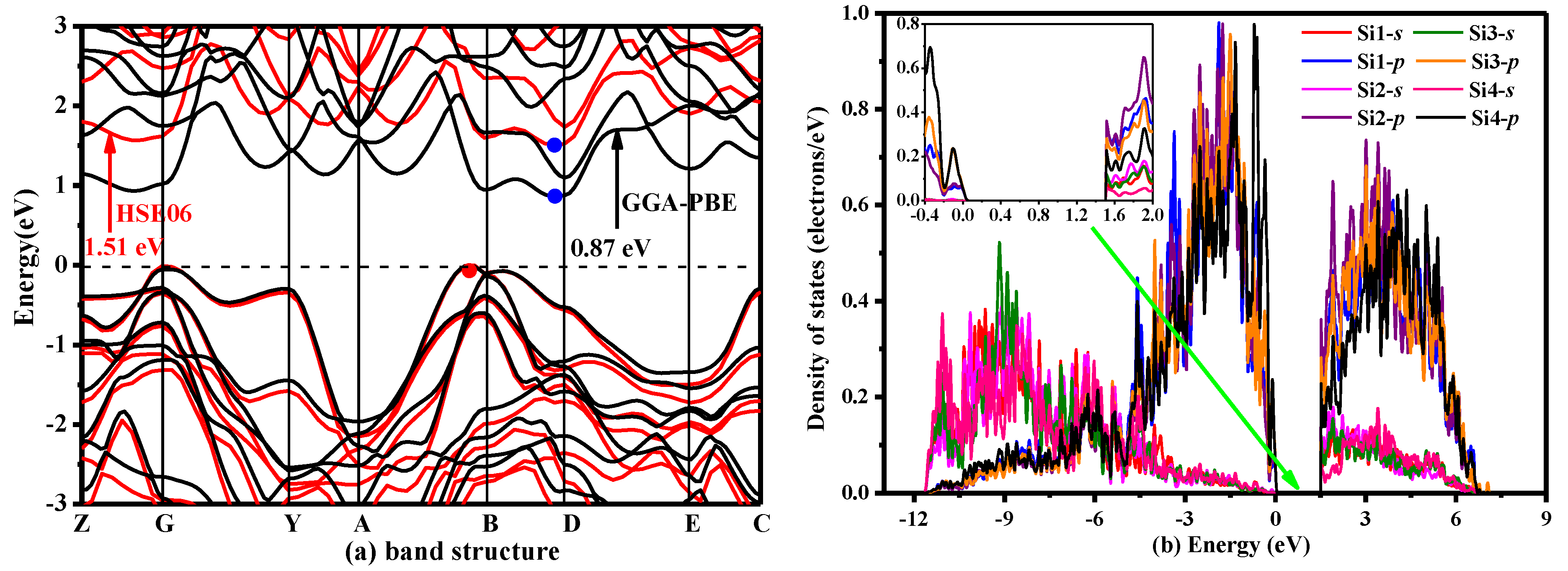
where the HF mixing parameter μ is 0.25 and the screening parameter ω is 0.207 Å−1 [44,45]. The electronic band structure of P2/m-Si was calculated using the GGA-PBE and HSE06 functionals, and the electronic band structures of P2/m-Si are shown in Figure 5a. Figure 5a clearly shows that P2/m-Si is an indirect-band-gap semiconductor with a band gap of 1.51 eV, as determined by the HSE06 hybrid functional. The result calculated by the HSE06 hybrid functional is much larger than the result from the GGA-PBE functional (0.87 eV). In addition, the band gap was found to be higher than that of diamond silicon by 0.23 eV using the same calculation method (diamond silicon: 1.28 eV [11,44]). Moreover, the band gap of diamond silicon calculated by HSE06 is very close to the experimental value (1.12 eV [11,30]). The charge effective mass, which is also a key physical property for applications, can be obtained by the formula m* = h2/(d2E/d2k) in which h is the planck constant, E is energy, k is wave vector. (m*n = 0.023m0, m*p = 0.019m0.). The effective mass reflects the carrier mobility indirectly (μ = qτ/m∗). The experimental effective mass at the Γ valley for a-GaN is 0.2m0 [46], while the effective mass for a hole in a-GaN at the valence band is 0.6m0. Besides, the effective mass at the Γ valley for GaAs is 0.0635m0 at the temperature 300 K [47]. The effective mass at the Γ valley for Ge is 0.038m0 at the temperature 300 K. The averaged light-hole mass in [001] is 0.046m0 [48]. The calculated effective mass of P2/m-Si is much smaller than that of GaN. Therefore, the mobility of P2/m-Si is larger than that of GaN, because the mobility is inversely proportional to the effective mass (μ = qτ/m∗). The electronic mobility of P2/m-Si is close to Ge. The density of states of P2/m-Si is displayed in Figure 5b, and the inset figure illustrates the local features at the Fermi level in detail. The dashed line represents the Fermi level. The DOS is divided into three regions: −13.5 eV to −5 eV, −5 eV to 0 eV and 0 eV to 7 eV. The lowest band ranging from −13.5 eV to −5 eV is characterized by the Si1-s, Si2-s, Si3-s and Si4-s orbitals. The middle band ranging from −5 eV to 0 eV is characterized by the Si1-p, Si2-p, Si3-p and Si4-p orbitals, and the upper band is also characterized by the Si1-p, Si2-p, Si3-p and Si4-p orbitals. In addition, the energy of the upper band is above 0.86 eV.
The thermodynamic properties of semiconductor materials at higher temperatures and pressures are interesting [38]. In this work, the highest pressure examined is 10 GPa, and the highest temperature is 1000 K. In the above conditions, the thermal expansion coefficient α, Grüneisen parameter γ and heat capacity were calculated. Figure 6 shows the thermal expansion coefficient α for P2/m-Si as functions of temperature and pressure. Figure 6a presents the relationship between the thermal expansion coefficient and pressure at different temperatures. The reduction in the amplitude decreases as the pressure increases, as shown in Figure 6a, and the difference in α is small at the same temperature. The reduction in amplitude at lower pressure is larger than that at higher pressure. However, the thermal expansion coefficient is constant when the temperature is 0 K (α = 0 × 10−5/K), and the difference in α between 600 K and 900 K (0.04 × 10⁻⁵/K at 0 GPa) is smaller than that between 300 K and 600 K (0.24 × 10⁻⁵/K at 0 GPa). As seen in Figure 6b, the thermal expansion coefficient increases quickly with increasing temperature, especially when the temperature is below 500 K. The increase in amplitude becomes very small when the temperature is over 500 K. Moreover, the thermal expansion coefficient increases less at increased pressure. Thus, by comparing Figure 6a with Figure 6b, it can be determine that the expansion coefficient α is more sensitive to the temperature when the temperature is below 500 K. From Figure 6, it is clear that the effect of pressure on the expansion coefficient α is not as significant as the effect of temperature over calculated pressure and temperature ranges.
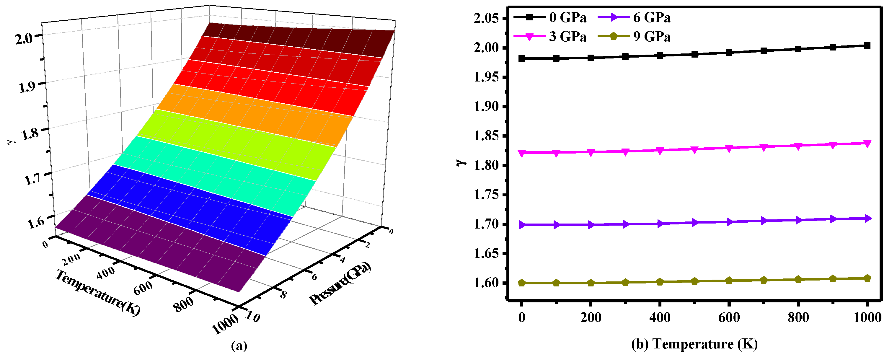
Figure 7 shows the change in the Grüneisen parameter γ with temperature and pressure, where the Grüneisen parameter γ is expressed as γ = −(dlnΘ(V)/dlnV) [49], where Θ is the Debye temperature and V is the volume. This parameter describes the anharmonic effects in the lattice vibrations [38]. As seen in Figure 7a, the γ parameter reduces by 0.045 per GPa, and the values are very close at different temperatures. In other words, the effect of pressure on the Grüneisen parameter γ is greater than that of temperature. As seen in Figure 7b, the γ parameter is not very sensitive to temperature. As the temperature increases to 1000 K, the Grüneisen parameter γ only increases by 0.02 at 6 GPa and 0.01 at 7 GPa or more.
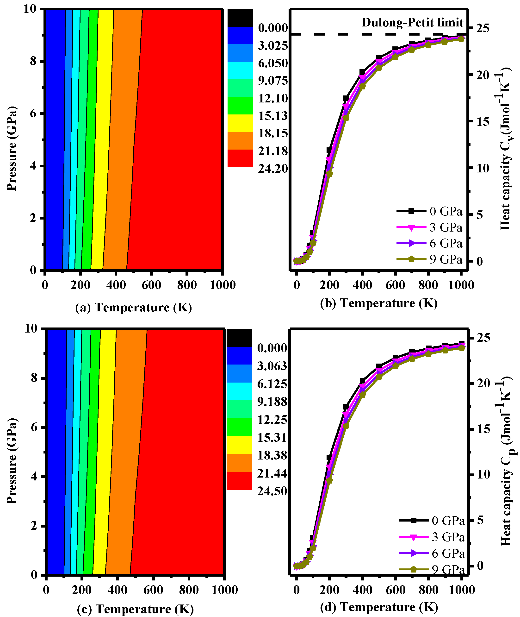
This study also examined the heat capacity at constant volume (CV) and constant pressure (CP) (Figure 8), which were calculated by the following formulas [38]:
where n is the number of atoms per formula unit, Θ is the Debye temperature, k is Boltzmann constant and D (Θ/T) represents the Debye integral [38]. As seen in Figure 8, the difference between CP and CV is very small. In addition, the trend is basically consistent with the trend at different pressures. Both plots increase as the temperature increases. It is obvious that the heat capacity is sensitive to temperature when T < 500 K; however, the magnitude of the increasement becomes very small when the temperature is over 500 K. In addition, the effect of pressure on the heat capacity is very small. CV stays close to constant at the Dulong-Petit limit (24.92 J·mol−1·K−1) [38] at high temperature and high pressure. Thus, the heat capacity of P2/m-Si is mainly affected by the temperature, and the effect of the pressure is small compared to that of the temperature.
4. Conclusions
This study predicts a new silicon allotrope with space group P2/m. The crystal structure, mechanical properties, elastic anisotropy, stability, electronic properties, and thermal properties of P2/m-Si were systematically studied. P2/m-Si is an indirect-band-gap semiconductor with a band gap of 1.51 eV, and Si in the P2/m phase is also mechanically, dynamically and thermally stabile at ambient pressures. The hardness was calculated to be 10.0 GPa, which is very close to that of diamond silicon. In addition, P2/m-Si is more brittle than the other allotropes of C2/m-16 Si, C2/m-20 Si, I-4 Si, and Amm2 Si. P2/m-Si also has larger anisotropy factors in different planes, especially for A3. P2/m-Si has the least anisotropy in its shear modulus, which is similar to diamond silicon, and the universal anisotropy of P2/m-Si is smaller than that of diamond silicon. High pressure leads to a smaller thermal expansion and a smaller Grüneisen parameter at ambient temperatures. Moreover, the lattice constants, Grüneisen parameter and the heat capacity have very small changes at different temperatures with increasing pressure. In addition, the heat capacity is nearly stable, showing value of 25 J·mol−1·K−1 when the temperature is higher than 800 K.
Acknowledgments
This work was supported by the Natural Science Foundation of China (No.61474089) and the Open Fund of the Key Laboratory of Complex Electromagnetic Environment Science and Technology, China Academy of Engineering Physics (No. 2015-0214. XY.K).
Author Contributions
Qingyang Fan designed the project; Qingyang Fan, Changchun Chai, and Chaogang Bai performed the calculations; Qingyang Fan, Changchun Chai, Chaogang Bai, and Yintang Yang analysed the results; and Chaogang Bai and Changchun Chai wrote the manuscript.
Conflicts of Interest
The authors declare no conflict of interest.
References
- Hao, X.P.; Cui, H.L. Electronic, elastic properties and hardness of the novel tetragonal silicon. J. Korean Phys. Soc. 2014, 65, 45–51. [Google Scholar] [CrossRef]
- Lee, I.H.; Lee, Y.J.; Oh, S.; Kim, K.J. Computational search for direct band gap silicon crystals. Phys. Rev. B 2014, 90, 115209. [Google Scholar] [CrossRef]
- Wu, F.; Dai, J.; Kan, E.J.; Li, Z.Y. Density functional predictions of new silicon allotropes: Electronic properties and potential applications to Li-battery anode materials. Solid State Commun. 2011, 151, 1228–1230. [Google Scholar] [CrossRef]
- Wang, Q.Q.; Xu, B.; Sun, J.; Liu, H.Y.; Zhao, Z.S.; Yu, D.L.; Fan, C.Z.; He, J.L. Direct band gap silicon allotropes. J. Am. Chem. Soc. 2014, 136, 9826–9829. [Google Scholar] [CrossRef] [PubMed]
- Fan, Q.Y.; Chai, C.C.; We, Q.; Yang, Y.T.; Chen, P.Y.; Xing, M.J.; Zhang, J.Q.; Yao, R.H. Prediction of novel phase of silicon and Si-Ge alloys. J. Solid State Chem. 2015, 233, 471–483. [Google Scholar] [CrossRef]
- Bateman, T.B.; Mcskimin, H.J.; Whelan, J.M. Elastic moduli of single crystal gallium arsenide. J. Appl. Phys. 1959, 30, 544–545. [Google Scholar] [CrossRef]
- Zhang, X.X.; Wang, Y.C.; Lv, J.; Zhu, C.Y.; Li, Q.; Zhang, M.; Ma, Y.M. First-principles structural design of superhard materials. J. Chem. Phys. 2013, 138, 114101. [Google Scholar] [CrossRef] [PubMed]
- Matt, L.; Joshua, G. Semiconductor nanowires and nanotubes. Annu. Rev. Mater. Res. 2004, 34, 83–122. [Google Scholar]
- Amsler, M.; Botti, S.; Marques, M.A.L.; Lenosky, T.J.; Goedecker, S. Low-density silicon allotropes for photovoltaic applications. Phys. Rev. B 2015, 92, 014101. [Google Scholar] [CrossRef]
- Fan, Q.Y.; Chai, C.C.; We, Q.; Yan, H.Y.; Zhao, Y.B.; Yang, Y.T.; Yu, X.H.; Liu, Y.; Xing, M.J.; Zhang, J.Q.; Yao, R.H. Novel silicon allotropes: Stability, mechanical, and electronic properties. J. Appl. Phys. 2015, 118, 4870–4876. [Google Scholar] [CrossRef]
- Wei, Q.; Zhang, Q.; Yan, H.Y.; Zhang, M.G. A new superhard carbon allotrope: Tetragonal C64. J. Mater. Sci. 2016, 52, 2385–2391. [Google Scholar] [CrossRef]
- Du, Y.; Zhuang, J.C.; Liu, H.; Xu, X.; Eilers, S.; Wu, K.; Cheng, P.; Zhao, J.; Pi, X.; See, K.; et al. Tuning the band gap in silicene by oxidation. ACS Nano 2014, 8, 10019. [Google Scholar] [CrossRef] [PubMed]
- Feng, B.; Ding, Z.; Meng, S.; Yao, Y.; He, X.; Cheng, P.; Chen, L.; Wu, K.H. Evidence of silicene in honeycomb structures of silicon on Ag (111). Nano Lett. 2012, 12, 3507–3511. [Google Scholar] [CrossRef] [PubMed]
- Du, Y.; Zhuang, J.C.; Wang, J.O.; Li, Z.; Liu, H.S.; Zhao, J.J.; Xu, X.; Feng, H.F.; Chen, L.; Wu, K.H.; et al. Quasi-freestanding epitaxial silicene on Ag (111) by oxygen intercalation. Sci. Adv. 2016, 2, e1600067. [Google Scholar] [CrossRef] [PubMed]
- Oh, Y.J.; Lee, I.H.; Kim, S.; Lee, J.; Chang, K.J. Dipole-allowed direct band gap silicon superlattices. Sci. Rep. 2015, 5, 18086. [Google Scholar] [CrossRef] [PubMed]
- Lee, I.H.; Oh, Y.J.; Kim, S.; Lee, J.; Chang, K.J. Ab initio, materials design using conformational space annealing and its application to searching for direct band gap silicon crystals. Comput. Phys. Commun. 2016, 203, 110–121. [Google Scholar] [CrossRef]
- Kim, D.Y.; Stefanoski, S.; Kurakevych, O.O.; Strobel, T.A. Synthesis of an open-framework allotrope of silicon. Nat. Mater. 2015, 14, 169–173. [Google Scholar] [CrossRef] [PubMed]
- Guo, Y.G.; Wang, Q.; Kawazoe, Y.; Jena, P. A new silicon allotrope with a direct band gap for optoelectronic applications. APS Meet. 2015, 5, 14342. [Google Scholar]
- Niu, H.; Chen, X.Q.; Wang, S.; Li, D.; Mao, W.L.; Li, Y. Families of superhard crystalline carbon allotropes constructed via cold compression of graphite and nanotubes. Phys. Rev. Lett. 2012, 108, 135501. [Google Scholar] [CrossRef] [PubMed]
- Botti, S.; Floreslivas, J.A.; Amsler, M.; Goedecker, S.; Marques, M.A.L. Low-energy silicon allotropes with strong absorption in the visible for photovoltaic applications. Phys. Rev. B 2012, 86, 7035–7040. [Google Scholar] [CrossRef]
- Hohenberg, P.; Kohn, W. Inhomogeneous electron gas. Phys. Rev. 1964, 136, B864. [Google Scholar] [CrossRef]
- Kohn, W.; Sham, L.J.P.R. The self-consistent field for molecular and solids. Phys. Rev. 1965, 140, A1133. [Google Scholar] [CrossRef]
- Clark, S.J.; Segall, M.D.; Pickard, C.J.; Hasnip, P.J.; Probert, M.I.J.; Refson, K.; Payne, M.C.; Krist, Z. First principles methods using CASTEP: Zeitschrift für Kristallographie-Crystalline materials. Z. Kristallogr. 2005, 220, 567. [Google Scholar] [CrossRef]
- Pfrommer, B.G.; Louie, S.G.; Cohen, M.L. Ab initio study of silicon in the R8 phase. Phys. Rev. B 1997, 56, 6662–6668. [Google Scholar] [CrossRef]
- Perdew, J.P.; Burke, K.; Ernzerhof, M. Generalized gradient approximation made simple. Phys. Rev. Lett. 1996, 77, 3865–3868. [Google Scholar] [CrossRef] [PubMed]
- Ceperley, D.M.; Alder, B.J. Ground state of the electron gas by a stochastic method. Phys. Rev. Lett. 1980, 45, 566–569. [Google Scholar] [CrossRef]
- Perdew, J.P.; Zunger, A. Self-interaction correction to density-functional approximations for many-electron systems. Phys. Rev. B 1981, 23, 5048–5079. [Google Scholar] [CrossRef]
- Baroni, S.; De Gironcoli, S.; Dal Corso, A.; Giannozzi, P. Phonons and related crystal properties from density-functional perturbation theory. Rev. Mod. Phys. 2001, 73, 515–562. [Google Scholar] [CrossRef]
- Hall, J.J. Electronic effects in the elastic constants of n-type silicon. Phys. Rev. 1967, 161, 756–761. [Google Scholar] [CrossRef]
- Shishkin, M.; Kresse, G. Self-consistent GW calculations for semiconductors and insulators. Phys. Rev. B 2007, 75, 235102. [Google Scholar] [CrossRef]
- Tan, L.; Chai, C.C.; Fan, Q.Y.; Yang, Y.T. Mechanical and electronic properties of C–Si alloys in the P2221 structure. Chin. J. Phys. 2016, 54, 700–710. [Google Scholar] [CrossRef]
- Wu, Z.J.; Zhao, E.J.; Xiang, H.P.; Hao, X.F.; Liu, X.J.; Meng, J. Crystal structures and elastic properties of superhard IrN2 and IrN3: From first principles. Phys. Rev. B 2007, 76, 054115. [Google Scholar] [CrossRef]
- Wortman, J.J.; Evans, R.A. Young’s modulus, shear modulus, and poisson’s ratio in silicon and germanium. J. Appl. Phys. 1965, 36, 153–156. [Google Scholar] [CrossRef]
- Zhang, Y.H.; Chai, C.C.; Fan, Q.Y.; Yang, Y.T. Mechanical and electronic properties of Si, Ge alloy in Cmmm, structure. Chin. J. Phys. 2016, 54, 298–307. [Google Scholar] [CrossRef]
- He, C.Y.; Zhang, C.X.; Li, J.; Peng, X.Y.; Meng, L.J.; Tang, C.; Zhong, J.X. Direct and quasi-direct band gap silicon allotropes with remarkable stability. Phys. Chem. Chem. Phys. 2016, 18, 9682–9686. [Google Scholar] [CrossRef] [PubMed]
- Fan, Q.Y.; Chai, C.C.; Wei, Q.; Zhou, P.K.; Zhang, J.Q.; Yang, Y.T. Si96: A new silicon allotrope with interesting physical properties. Materials 2016, 9, 284. [Google Scholar] [CrossRef]
- Pugh, S.F. Relations between the elastic moduli and the plastic properties of polycrystalline pure metals. Philos. Mag. 1954, 45, 823–843. [Google Scholar] [CrossRef]
- Fan, Q.Y.; Wei, Q.; Yan, H.Y.; Zhang, M.G.; Zhang, J.Q. A new potential superhard phase of OsN2. Acta Phys. Pol. A 2014, 126, 740–747. [Google Scholar] [CrossRef]
- Hill, R. The elastic behaviour of a crystalline aggregate. Proc. Phys. Soc. Lond. 1952, 65, 349–354. [Google Scholar] [CrossRef]
- Fan, Q.Y.; Wei, Q.; Yan, H.Y.; Zhang, M.G.; Zhang, Z.X.; Zhang, J.Q.; Zhang, D.Y. Elastic and electronic properties of pbca-bn: First-principles calculations. Comp. Mater. Sci. 2014, 85, 80–87. [Google Scholar] [CrossRef]
- Damay, F.; Poienar, M.; Hervieu, M. High-pressure polymorph of LuFe2O4, with room-temperature antiferromagnetic order. Phys. Rev. B 2015, 91, 214111. [Google Scholar] [CrossRef]
- Connétable, D.; Thomas, O. First-principles study of the structural, electronic, vibrational, and elastic properties of orthorhombic nisi. Phys Rev. B 2009, 79, 094101. [Google Scholar] [CrossRef]
- Heyd, J.; Scuseria, G.E.; Ernzerhof, M. Hybrid functionals based on a screened Coulomb potential. J. Chem. Phys. 2003, 118, 8207–8215. [Google Scholar] [CrossRef]
- Heyd, J.; Scuseria, G.E.; Ernzerhof, M. Hybrid functionals based on a screened Coulomb potential. J. Chem. Phys. 2006, 118, 8207–8215. [Google Scholar] [CrossRef]
- Krukau, A.V.; Vydrov, O.A.; Izmaylov, A.F.; Scuseria, G.E. Influence of the exchange screening parameter on the performance of screened hybrid functional. J. Chem. Phys. 2007, 125, 224106. [Google Scholar] [CrossRef] [PubMed]
- Monemar, B. III-V nitrides—Important future electronic materials. J. Mater. Sci. 1999, 10, 227–254. [Google Scholar]
- Szmyd, D.M.; Porro, P.; Majerfeld, A.; Lagomarsino, S. Heavily doped GaAs:Se. I. Photoluminescence determination of the electron effective mass. J. Appl. Phys. 1990, 68, 2367–2375. [Google Scholar] [CrossRef]
- Burstein, E.; Picus, G.S.; Wallis, R.F.; Blatt, F. Zeeman-type magneto-optical studies of interband transitions in semiconductors. Phys. Rev. 1959, 113, 15–33. [Google Scholar] [CrossRef]
- Basile, G.; Bergamin, A.; Cavagenro, G.; Mana, E.; Vittone, G.; Zosi. Measurement of the silicon (220) lattice spacing. Phys. Rev. Lett. 1994, 72, 3133–3136. [Google Scholar] [CrossRef] [PubMed]
Figure 1.
(a) Unit cell crystal structures of P2/m-Si; (b) The structural view along the [010] direction; (c) The structural view along the [100] direction.
Figure 1.
(a) Unit cell crystal structures of P2/m-Si; (b) The structural view along the [010] direction; (c) The structural view along the [100] direction.
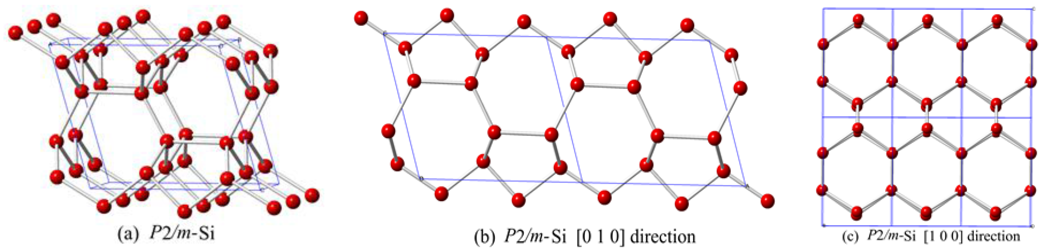
Figure 2.
(a) The lattice constants a/a0, b/b0, and c/c0 during compression as functions of pressure for P2/m-Si; (b) The lattice constants a/a0, b/b0, and c/c0 during compression as functions of temperature for P2/m-Si.
Figure 2.
(a) The lattice constants a/a0, b/b0, and c/c0 during compression as functions of pressure for P2/m-Si; (b) The lattice constants a/a0, b/b0, and c/c0 during compression as functions of temperature for P2/m-Si.
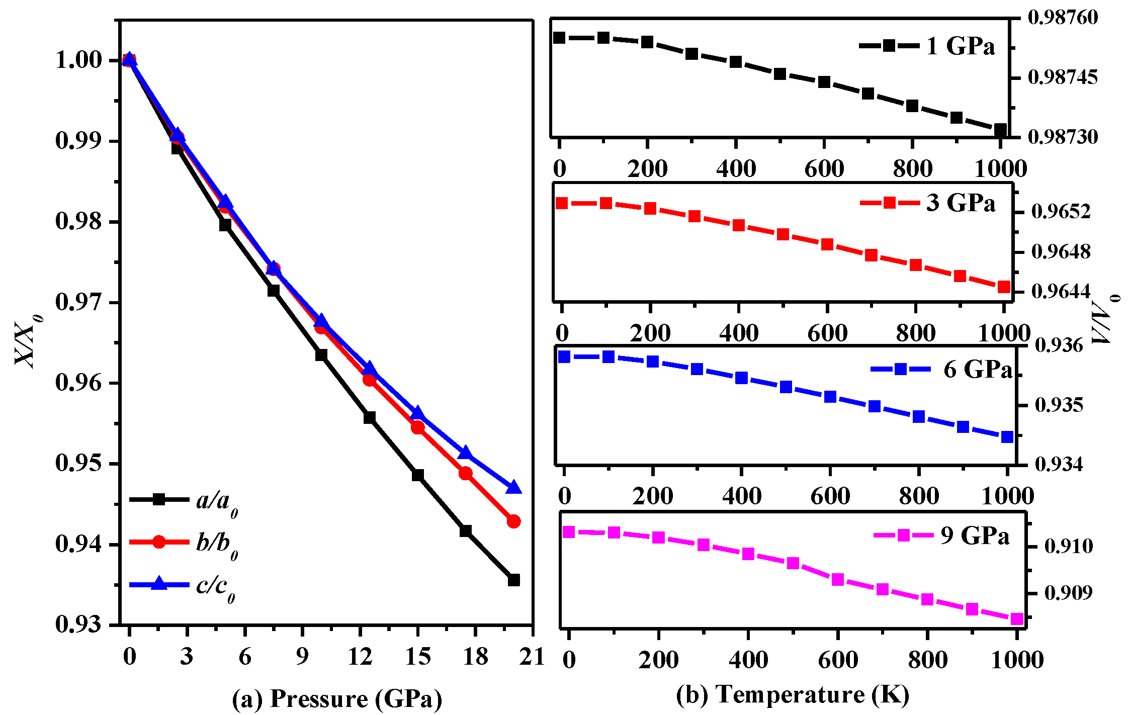
Figure 3.
Phonon spectra for P2/m-Si at different pressures: (a) 0 GPa and (b) 20 GPa.
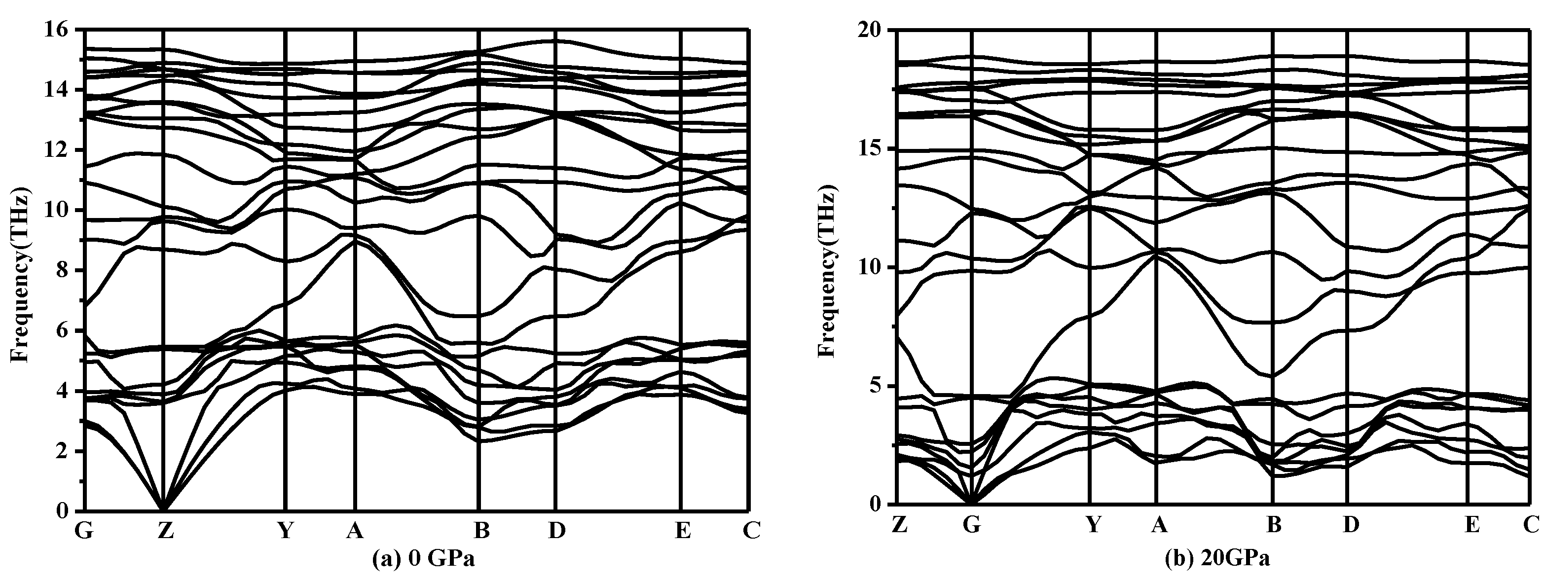
Figure 4.
The calculated enthalpies of different silicon structures as a function of pressure.
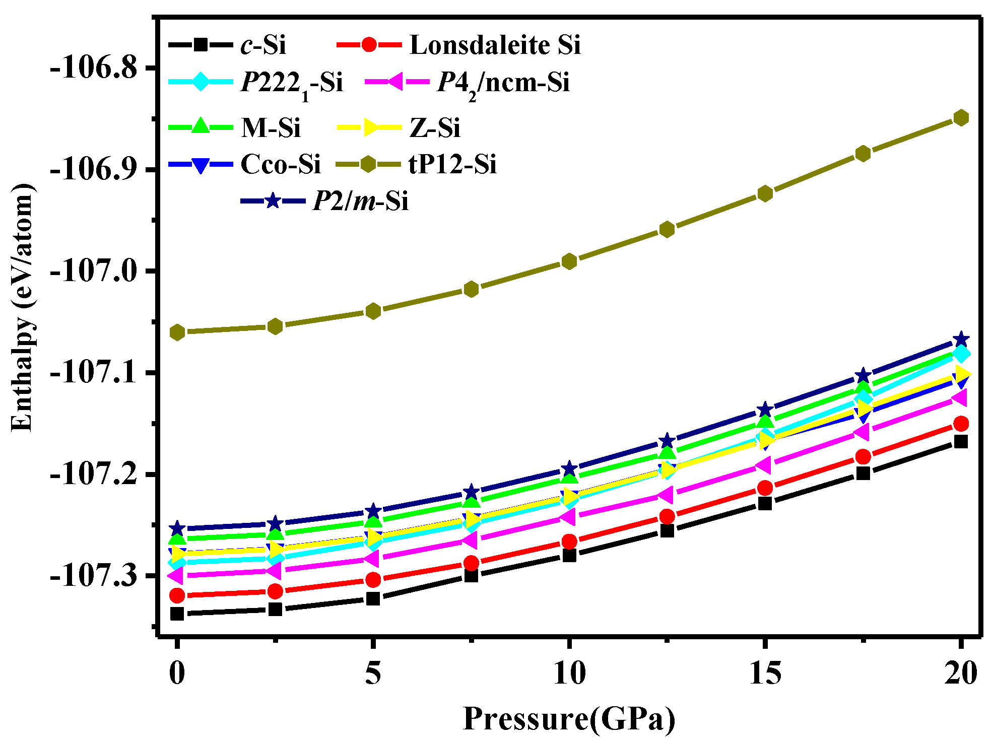
Figure 5.
(a) Electronic band structure and (b) density of states of P2/m-Si.

Figure 6.
(a) Pressure dependence of the thermal expansion coefficient for P2/m-Si; (b) Temperature dependence of the thermal expansion coefficient for P2/m-Si.
Figure 6.
(a) Pressure dependence of the thermal expansion coefficient for P2/m-Si; (b) Temperature dependence of the thermal expansion coefficient for P2/m-Si.
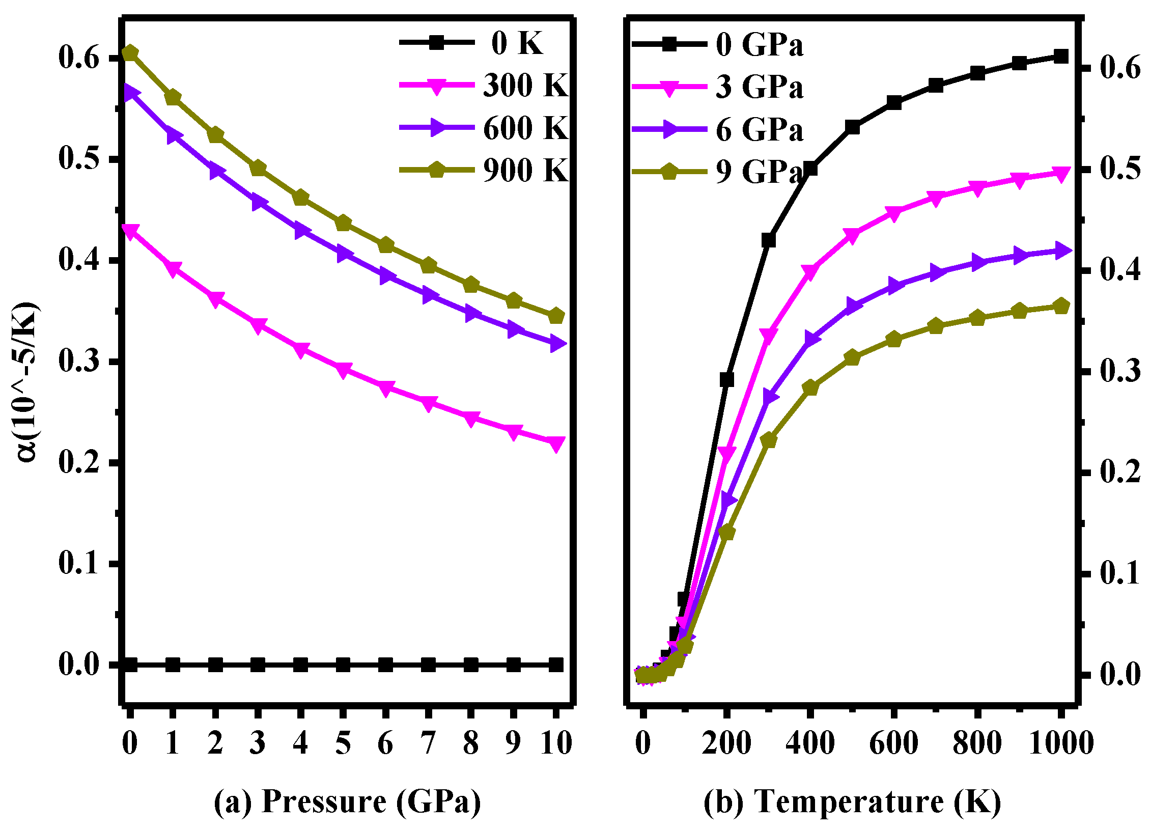
Figure 7.
(a) Three-dimensional contour plot of the Grüneisen parameter versus pressure and temperature for P2/m-Si; (b) Temperature dependence of the Grüneisen parameter for P2/m-Si.
Figure 7.
(a) Three-dimensional contour plot of the Grüneisen parameter versus pressure and temperature for P2/m-Si; (b) Temperature dependence of the Grüneisen parameter for P2/m-Si.

Figure 8.
Calculated specific volume CV and pressure heat capacity CP as a function of pressure for P2/m-Si at different temperatures: (a) CV contours; (b) CV–T; (c) CP contours; and (d) CP–T.
Figure 8.
Calculated specific volume CV and pressure heat capacity CP as a function of pressure for P2/m-Si at different temperatures: (a) CV contours; (b) CV–T; (c) CP contours; and (d) CP–T.

Table 1.
The lattice parameters (Å) of different space groups calculated by different methods.
| Method | PBE | PBEsol | CA-PZ | |||||||||
|---|---|---|---|---|---|---|---|---|---|---|---|---|
| Space Group | a | b | c | β | a | b | c | β | a | b | c | β |
| P2/m | 7.253 | 3.868 | 6.294 | 105.9 | 7.243 | 3.861 | 6.283 | 105.8 | 7.136 | 3.802 | 6.187 | 105.8 |
| P2221 | 5.429 | 13.112 | 5.265 | - | 5.334 | 12.98 | 5.211 | - | 5.349 | 12.758 | 5.264 | - |
| P2221 c | 5.448 | 13.017 | 5.339 | - | 5.445 | 12.995 | 5.327 | - | 5.364 | 12.803 | 5.248 | - |
| P2221 | 7.495 | 5.359 | 5.410 | - | 7.477 | 5.432 | 5.316 | - | 7.345 | 5.379 | 5.258 | - |
| P2221 f | 7.487 | 5.450 | 5.221 | - | 7.487 | 5.446 | 5.206 | - | 7.365 | 5.373 | 5.123 | - |
| Fd-3m | a = 5.426, 5.402 a, 5.429 e, 5.465 b, 5.431 d | a = 5.466 | a = 5.374, 5.392 a | |||||||||
Table 2.
The calculated elastic constants Cij, bulk modulus B, shear modulus G, Young’s modulus E, and Poisson’s ratio v of different silicon allotropes (GPa) (S.G.: space group).
Table 2.
The calculated elastic constants Cij, bulk modulus B, shear modulus G, Young’s modulus E, and Poisson’s ratio v of different silicon allotropes (GPa) (S.G.: space group).
| S.G. | Method | C11 | C22 | C33 | C44 | C55 | C66 | C12 | C13 | C15 | C23 | C25 | C35 | C46 | B | G | B/G | E | v |
|---|---|---|---|---|---|---|---|---|---|---|---|---|---|---|---|---|---|---|---|
| P2/m | GGA | 159 | 167 | 150 | 63 | 55 | 40 | 29 | 42 | −1 | 51 | 9 | 2 | 8 | 80 | 54 | 1.48 | 132 | 0.22 |
| LDA | 171 | 176 | 160 | 61 | 57 | 40 | 35 | 50 | 0 | 58 | 10 | 3 | 8 | 88 | 54 | 1.63 | 134 | 0.25 | |
| C2/m-16 a | GGA | 146 | 146 | 164 | 48 | 53 | 53 | 51 | 47 | - | 43 | - | - | - | 82 | 51 | 1.61 | 127 | 0.24 |
| C2/m-20 a | GGA | 184 | 167 | 143 | 55 | 52 | 52 | 36 | 46 | - | 46 | - | - | - | 83 | 55 | 1.51 | 135 | 0.23 |
| I-4 a | GGA | 142 | 142 | 145 | 57 | 47 | 55 | 48 | 50 | - | 50 | - | - | - | 80 | 48 | 1.68 | 120 | 0.25 |
| Amm2 a | GGA | 161 | 179 | 131 | 44 | 44 | 51 | 37 | 42 | - | 38 | - | - | - | 78 | 51 | 1.54 | 126 | 0.23 |
| Fd-3m | GGA | 154 | - | - | 79 | - | - | 56 | - | - | - | - | - | - | 88 | 64 | 1.38 | 155 | 0.21 |
| - | LDA | 163 | - | - | 80 | - | - | 58 | - | - | - | - | - | - | 93 | 68 | 1.37 | 164 | 0.21 |
| - | Exp. b | 166 | - | - | 80 | - | - | 64 | - | - | - | - | - | - | 102 | - | - | - | - |
Table 3.
The excess formation enthalpy of different silicon allotropes relative to diamond silicon under 0 GPa. (eV). And n represents the Si (111)n/Si(SC) superlattices with the cubic- and hexagonal-stacking sequences of Si (111) layers (SM: simple monoclinic, SO: simple orthorhombic, and BCO: base-centered orthorhombic).
| Diamond Si a | Lonsdaleite a | M a | Cco a | P2221 a | P42/ncm a | Z a | tP12 a | P2/m | P21/m b |
| 0.00 | 0.02 | 0.08 | 0.06 | 0.05 | 0.04 | 0.06 | 0.28 | 0.09 | 0.02 |
| Imma b | Pbam b | Pmmn b | Cmcm b | P-1 c | P21/c c | C2/m-16 a | C2/m-20 a | I-4 a | Amm2 a |
| 0.07 | 0.06 | 0.08 | 0.04 | 0.13 | 0.14 | 0.13 | 0.10 | 0.10 | 0.11 |
| n = 1 (BCO) d | n = 2 (SM) d | n = 3 (SM) d | n = 4 (SM) d | n = 5 (SM) d | n = 6 (SM) d | n = 7 (SM) d | n = 8 (SM) d | n = 9 (SM) d | n = 10 (SM) d |
| 0.09 | 0.05 | 0.04 | 0.03 | 0.03 | 0.02 | 0.02 | 0.02 | 0.02 | 0.01 |
| n = 2 (SO) d | n = 3 (SM) d | n = 4 (SO) d | n = 5 (SM) d | - | - | - | - | - | - |
| 0.07 | 0.05 | 0.03 | 0.03 | - | - | - | - | - | - |
Table 4.
The compression and shear anisotropy percent factors (AB and AG), universal anisotropy indexes (AU) and shear anisotropy factors (A1, A2 and A3) of different structures.
Table 4.
The compression and shear anisotropy percent factors (AB and AG), universal anisotropy indexes (AU) and shear anisotropy factors (A1, A2 and A3) of different structures.
| Space Group | AB | AG | AU | A1 | A2 | A3 |
|---|---|---|---|---|---|---|
| P2/m | 0.000 | 0.028 | 0.269 | 1.056 | 1.036 | 0.578 |
| Amm2 a | 0.641 | 1.359 | 0.151 | 0.839 | 0.750 | 0.766 |
| C2/m-16 a | 0.128 | 1.475 | 0.152 | 0.881 | 0.940 | 1.111 |
| C2/m-20 a | 0.347 | 1.971 | 0.208 | 0.937 | 0.954 | 0.752 |
| I-4 a | 0.014 | 0.691 | 0.070 | 1.006 | 1.006 | 1.167 |
| Fd-3m a | 0.000 | 3.500 | 0.336 | 0.773 | 0.773 | 0.773 |
a Ref. [10].
© 2017 by the authors. Licensee MDPI, Basel, Switzerland. This article is an open access article distributed under the terms and conditions of the Creative Commons Attribution (CC BY) license (http://creativecommons.org/licenses/by/4.0/).
Share and Cite
MDPI and ACS Style
Bai, C.; Chai, C.; Fan, Q.; Liu, Y.; Yang, Y. A Novel Silicon Allotrope in the Monoclinic Phase. Materials 2017, 10, 441. https://doi.org/10.3390/ma10040441
AMA Style
Bai C, Chai C, Fan Q, Liu Y, Yang Y. A Novel Silicon Allotrope in the Monoclinic Phase. Materials. 2017; 10(4):441. https://doi.org/10.3390/ma10040441
Chicago/Turabian StyleBai, Chaogang, Changchun Chai, Qingyang Fan, Yuqian Liu, and Yintang Yang. 2017. "A Novel Silicon Allotrope in the Monoclinic Phase" Materials 10, no. 4: 441. https://doi.org/10.3390/ma10040441
Note that from the first issue of 2016, this journal uses article numbers instead of page numbers. See further details here.