The Impact of Graphene on the Fabrication of Thin Film Solar Cells: Current Status and Future Prospects

Nanotechnology and MEMS Laboratory, Department of Mechanical, Industrial, and Manufacturing Engineering (MIME), University of Toledo, Toledo, OH 43606, USA
*
Author to whom correspondence should be addressed.
Materials 2018, 11(1), 36; https://doi.org/10.3390/ma11010036
Submission received: 11 November 2017
/
Revised: 22 December 2017
/
Accepted: 27 December 2017
/
Published: 27 December 2017
(This article belongs to the Special Issue Graphene/Carbon Nanotubes Application in Solar Cells)
Abstract
:Commercial solar cells have a power conversion efficiency (PCE) in the range of 10–22% with different light absorbers. Graphene, with demonstrated unique structural, physical, and electrical properties, is expected to bring the positive effects on the development of thin film solar cells. Investigations have been carried out to understand whether graphene can be used as a front and back contacts and active interfacial layer in solar cell fabrication. In this review, the current progress of this research is analyzed, starting from the graphene and graphene-based Schottky diode. Also, the discussion was focused on the progress of graphene-incorporated thin film solar cells that were fabricated with different light absorbers, in particular, the synthesis, fabrication, and characterization of devices. The effect of doping and layer thickness of graphene on PCE was also included. Currently, the PCE of graphene-incorporated bulk-heterojunction devices have enhanced in the range of 0.5–3%. However, device durability and cost-effectiveness are also the challenging factors for commercial production of graphene-incorporated solar cells. In addition to the application of graphene, graphene oxides have been also used in perovskite solar cells. The current needs and likely future investigations for graphene-incorporated solar cells are also discussed.
1. Introduction
Graphene has attracted a great deal of attention in connection with nanotechnology since 2004 [1]. A perfect graphene sheet is only one-atom thick. Its atoms are arranged in a hexagonal structure, where atoms are all covalent bonded, which brings graphene superior mechanical strength (Young’s modulus exceed 1 TPa) [2]. After a decade’s intensive study, graphene has been already demonstrated with high carrier mobility (2 × 105 cm2/V·s for suspended graphene) at the room temperature [3], great transparency (~2.3% light absorption across most ultraviolet (UV) and visible spectrum) [4], high thermal conductivity (~103 W/m·K) [5] and high melting point (around 5000 K) [6]. Besides, the atom-layer structure also leads to a large surface area and great flexibility of graphene sheets. Thus, the low-cost graphene has been found in a wide range of applications, such as chemical sensors [7,8], medical devices [9], photo-detectors [10], energy storage [11], and manufacturing roll-to-roll electronic devices [12].
At present, a number of techniques have been developed for the fabrication of graphene. Besides the initial mechanical exfoliation of highly-organized graphite sheets [1], chemical vapor deposition (CVD) [13,14,15], supersonic spray [16], laser [17], and many other approaches have been established. Since graphene/graphene oxide (GO) is one-atom thick, conventional chemical synthesis that cannot be used for the production of graphene. Also, a substrate is necessary for growing graphene layers. Currently, the mainstream of graphene synthesis is still through the CVD method, which is popular in both academia and industries. In addition, the major synthesis path of GO and reduced graphene oxide (r-GO) is still the Hummer’s method [18] with different modifications on reaction conditions.
Solar energy conversion is another major area where graphene appears frequently. While the current photovoltaic (PV) market is still dominated by Si-based solar cells, thin film PVs that are based on CdTe [19,20], copper-indium-gallium sulfide (CIGS) [21], copper-zinc-tin sulfide (CZTS) [22,23], perovskite [24,25], and FeS2 [26] have been demonstrated with great potential. Lab-scale thin film PV devices have already reached 22% [24]. Thin film PV modules have also started the commercialization process and Si-based PV efficiency is getting closer to its theoretical upper limit [27]. On considering the high transparency, high carrier mobility, and conductivity, graphene has been tried as both contacts and interface layers in almost all kinds of PVs (e.g., Si, thin film, organic). In this review, we focused on the application of graphene on most commonly used thin-film PVs, with discussions on research advancement and the impact of graphene on those thin film PVs. The intention of this review is to improve scientific understanding of graphene properties that are relevant to PV applications and to accelerate the technological developments in the field.
2. Graphene and Graphene-Based Schottky Diodes
The microstructure of graphene consists of a repeatable two-dimensional (2D) hexagonal lattice. Each peak position is occupied by carbon atom, with another equivalent three covalent-bonded nearest neighbors, as shown in Figure 1a, where the corresponding primitive lattice vectors aree also labeled. Thus, the reciprocal lattice and the hexagonal Brillouin zone could be inferred, as shown in Figure 1b. together with the band structure of graphene. It is clear that the conduction and valence bands are attached at the two crystal momentum corners of the hexagonal Brillouin zone. Thus, the band gap of primitive graphene is zero (at K-K’), which is shown in Figure 1b, and graphene could be considered as a semi-metal.
When in contact graphene with a semiconductor, a Schottky junction would be formed. However, the Fermi level of graphene could be easily shifted by chemical doping or carrier injection under a bias [28,29]. Therefore, unlike the typical metal/semiconductor Schottky junction, the graphene/semiconductor could have a modified Schottky barrier height. Some early-stage experimental results claimed the formation of Schottky diode on various substrates, such as Si [30,31], GaAs [32], and SiC [33]. A strong rectifying behavior could be observed from their current-voltage (I-V) characteristics. Further calculation that is based on capacitance-voltage (C-V) measurement gave an estimation of graphene work function to be in the range of 4.4–4.8 eV [34].
Moreover, Riazimehr et al. [36] measured a photocurrent of graphene/n-Si Schottky diode and observed a light-generated current as shown in Figure 2a, indicating the photogeneration of electron-hole (e-h) in Si and the carrier extraction ability of graphene. Further investigation of mapping the position of incident light at a different location resulted in an effective load across the junction due to the different photocurrent with the corresponding light incident position. The resulting current–voltage characteristics exhibit rectifying diode behavior, with a barrier energy of 0.41 eV on n-type Si and 0.45 eV on p-type Si at the room temperature. Since Si is the most typical sunlight absorber, the contact nature of graphene with other thin-film PV materials could follow the similar behavior, as seen in Figure 2b. Also, energy band diagram of Graphene/n-Si is shown in Figure 2c.
3. Research Progress of Graphene-Composited Thin Film Solar Cell
3.1. Graphene with CdTe
With high transparency, carrier mobility and flexibility, graphene was first considered to be the alternative contact material. To the best of our knowledge, the first successful graphene-encountered CdTe device was reported by Bi et al. [37] with consideration of similar work function between graphene and fluorine doped tin oxide (FTO) [38]. In their work, the graphene was synthesized on a Cu foil by an atmospheric pressure CVD (APCVD) and later transferred to a glass substrate. By altering the H2 flow rate, the number of graphene layers could be well controlled, which also provides a wide selection range of transparency and sheet resistance. Two devices, with and without ZnO blocking layer, were fabricated and characterized. The device with ZnO layer showed a higher efficiency (4.17%) than the one without ZnO (2.81%), indicating the importance of ZnO: a good contact with graphene and current leakage protection. Followed by their initial work, this group reported a great advantage of the graphene-CdTe device with graphene as the back contact. In order to provide a better coverage and contact on CdTe, the graphene was synthesized with a three-dimensional (3D) structure using porous Ni foam as the growth substrate. A similar method was employed to grow graphene and the 3D structure was successfully observed and transferred to CdTe device. The final graphene back contact thickness exceeded 10 µm with an excellent electrical conductivity (550–600 S/cm), which assisted a significant device efficiency improvement up to 9.1%, as shown in Figure 3. Moreover, with a relatively large active area (1.0 cm2), this work indicated the possibility of large-scale device fabrication [39].
Moreover, graphene-based composite back contact was also tried: Liang et al. [40] reported the usage of Cu nanowire/graphene back contact for CdTe solar cell. Their graphene was also prepared with similar method [39], and then mixed with hydrothermally synthesized Cu nanowires. The mixture was brushed onto the CdTe layer and the device exhibited an efficiency of 12.1%, which, according to their comparison, was higher than single Cu and graphene back contact (see Table 1). This result might be related to a better hole collection process of graphene 3D network and the formation of the ultrathin CuTe interface layer. However, with an extra heating process on the device, the efficiency was decreased due to the lower thermal stability of graphene contact. It is important to prepare graphene layer without the interfering of oxidation species. There is no indication of any reactivity between Te and carbon, while Cu has the lowest solubility in carbon, which prevents the formation of any oxide layer. Thus, a decrease of efficiency of annealed device could be attributed to the interference of oxygen in graphene/CdTe interface.
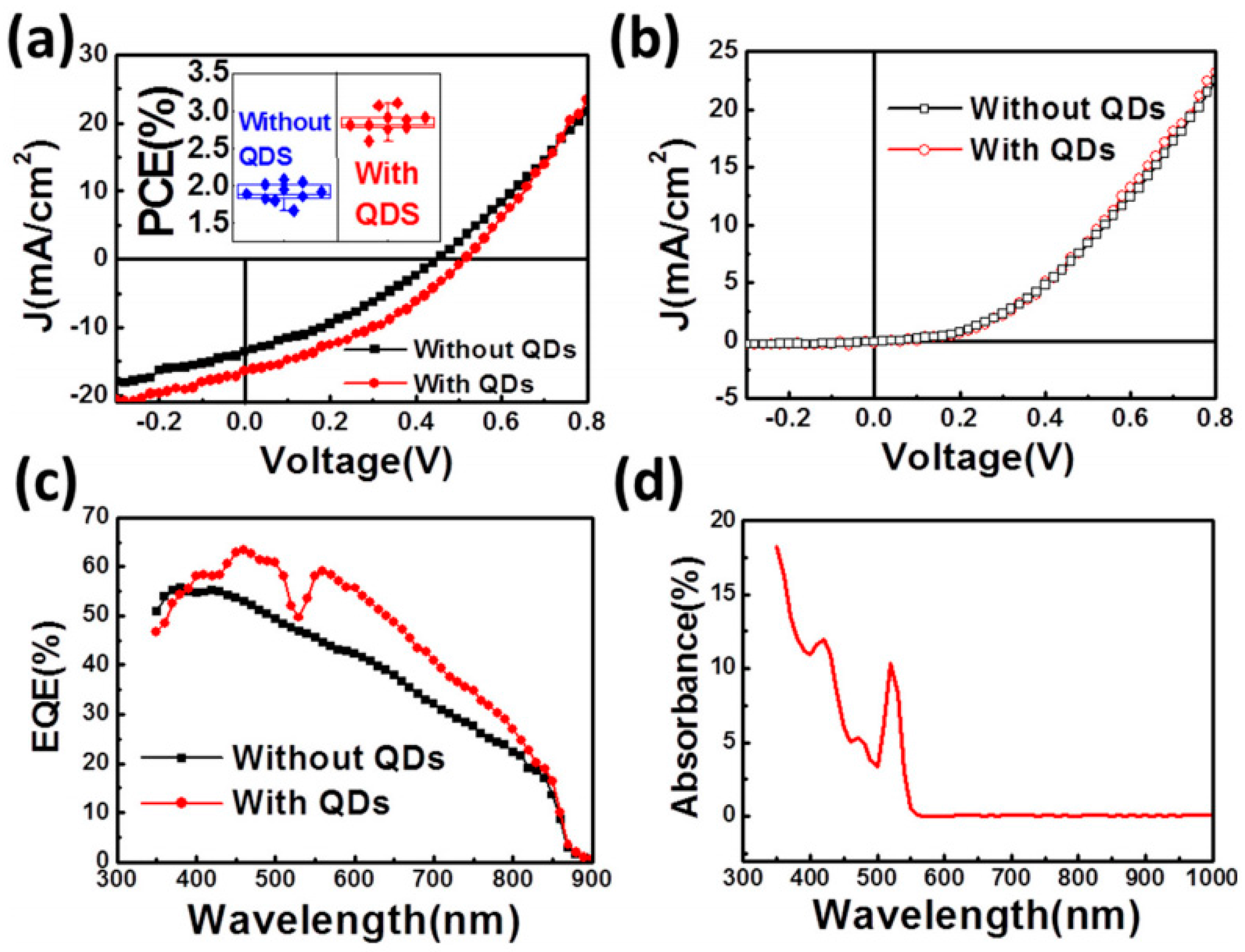
In addition, impurity doping into graphene was also tried in back contacts. One example is the comparison among boron-doped graphene, intrinsic graphene and reduced graphene oxide (r-GO) [41]. These results showed the boron-doped graphene back contact was the best choice due to the highest conductivity. This could be due to extra holes introduced into graphene through boron doping during the initial graphene synthesis. In addition to the efforts on applying graphene as the front and back contacts, trials of using graphene to replace CdS inside the CdS/CdTe system were also processed. Ideally, the work function of graphene is close to the electron affinity of CdTe, indicating a possible junction formation. According to Brus et al. [42], their graphite/n-CdTe (fabricated with the Cd-rich atmosphere) was able to acquire an efficiency of 1.36%, with a clear shunting effect. Later, Lin et al. [43] announced an unusual substrate-configured graphene/CdTe device. In this work, the graphene was synthesized by a CVD process and was transferred on to both CdTe and patterned SiNx, which served as a separator between Ag top grid and CdTe. Their device acquired a relatively high efficiency of 2.08%. Moreover, to test the importance of original window layer CdS/CdSe, a separately-prepared CdSe quantum dots was prepared and coated onto the graphene supporting layer, which elevated the efficiency result to 3.1%. Those extra n-type quantum dots also contributed to light-generated electron collecting, which led to a clear increase in both short-circuit current density (Jsc) and external quantum efficiency (EQE), as shown in Figure 4.
In addition to the above experimental results, simulation work also indicated the great potential in the application of graphene in CdTe system. Aldosari et al. [44] established a model with graphene at both front and back contact. They claimed that graphene front contact, with lower thickness, would lead to less incident current loss. Thus, mono-layer graphene would be the best choice. Also, the combination with ZnO would significantly improve the overall conductivity. For the back contact case, besides the proper work function of graphene, its appearance also made the double-sided illumination possible for CdTe solar cell. Therefore, the Jsc would be greatly enhanced and the CdTe thickness could also be reduced to around 1 µm to minimize unnecessary carrier generation. This group also claimed that the dangling bonds between graphene networks might generate movable ions, especially with the co-existence of metal dopant. Those free ions would diffuse into the p-n junction interface, and, therefore, cause damage to the device rather than at the back contact interface [45]. In addition, several reports related to the application of single-wall carbon nanotube were also indicated with a better device efficiency up to 14.1% [46]. More detailed information could be available from another review [47].
Although graphene was already demonstrated with great transparency and conductivity, the actual practice showed that more work is required to optimize the growth conditions, such as growth atmosphere profile and metallic doping, as well as their effects on graphene contact properties. Also, understanding of the thermal stability of graphene and graphene composite is also necessary. Overall, that reported progress showed that graphene could be a suitable replacement for FTO and metal back contact for CdTe system with a lower cost and easy manufacturing.
3.2. Graphene with CIGS
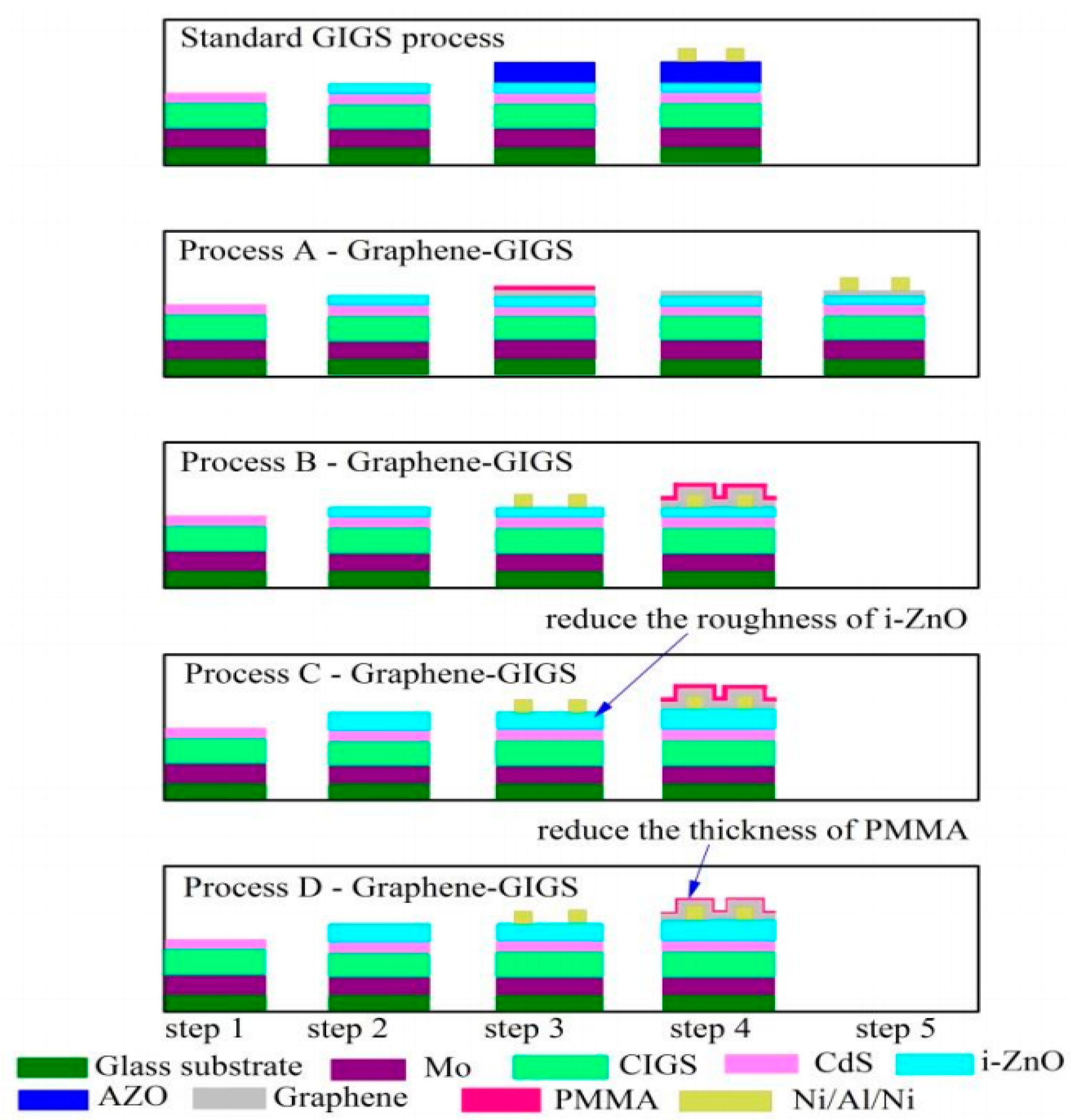
Similar to the CdTe system, graphene was first considered as an alternative front contact. Yin et al. [48] first reported an effort of replacing AZO with graphene or graphene/PMMA composite. Their results showed that the direct contact between graphene and i-ZnO was poor due to surface damage during PMMA removal, which also affects carrier collection through evaporated metal grids. Thus, they optimized the fabrication process, as shown in Figure 5 [48]. In this study, all possible CIGS solar cells have been described and the graphene has been incorporated at step-4 in all of the processes, except for standard process. Finally, the sheet resistance was minimized and they acquired a significant efficiency increase from the initial 0.43% to 13.5% as listed in Table 2. Those devices also showed better optical properties than the reference. However, the best result still had a small gap with their reference copper indium gallium sulfide (CIGS) device fabricated with AZO layer (Eff. 14.9%) probably due to a lower sheet resistance. They also believe that the graphene/PMMA could be a moisture protection of the CIGS solar cell.
Moreover, the Brookhaven National Lab achieved a direct n-doped graphene/CIGS Schottky junction [49]. The strong n-type doping on graphene was accomplished through Na diffusion from soda-lime glass (SLG) substrate through CIGS grain boundaries, which is similar to the ion migration in CdTe layer. When under standard AM 1.5G light, this device displayed a high photocurrent and a typical rectifying behavior. The Jsc was about 13 mA/cm2 and the efficiency was around 1%. However, the strong Na diffusion would affect the p-type region, which may affect the built-in potential and the open-circuit voltage (Voc) of the device.
According to the literature, very limited investigations have been carried out regarding the successful application of graphene as the back contact for CIGS although the work function requirement was similar to CdTe. But, a simulation work based on refractive index and extinction coefficient indicated that the graphene back contact would lead to a higher Jsc and efficiency than the front contact case [50]. As predicted in the CdTe model, the high-transparent graphene contact would enable double-side illumination on the solar cell, which may create efficiency that similar to the dominant Si-based solar cells. The successful 3D dimension of graphene back contact on CdTe might be a good reference for developing similar layer for CIGS.
At present, no experimental record shows the effect of graphene on copper-zinc-tin sulfide (CZTS) system. Only a simulation result predicted the advantage of using graphene front contact, rather than the conventional indium-tin-oxide (ITO) [51]. In their work, such replacement was believed to increase all of the solar cell parameters, as well as further minimizing the CZTS absorber thickness. In addition, researchers also demonstrated the successful synthesis of copper indium sulfide (CIS) films on graphene contacts. The CIS films fabricated on graphene layers, rather than on Mo contacts, showed a strong preferential growth in (112) direction. A strong ohmic contact was also identified [52]. Another study focused on copper tin sulfide (CTS) synthesis on r-GO and their results showed that CTS/r-GO could be a great photo-conductor. With the addition of ethylenediaminetetraacetic acid as the complexing agent during initial synthesis, the photocurrent could be enhanced by 60% [53]. Those discoveries indicate a great potential of graphene application on the photo-sensitive ternary phases of CIGS and CZTS.
The above information, it could be inferred that the application of graphene on CIGS or its relevant materials system is still in its early stage. Similar to CdTe case, more understanding and experience are required for the optimization of transport phenomenon at the GIGS/graphene interface. Based on the current literature, it can be expected that the performance of CIGS solar cells will be further enhanced by the application of graphene.
3.3. Graphene with Perovskite
In the past few years, the organic-inorganic lead-halide perovskite solar cells (PSCs) achieved fast efficiency improvement from 3.8% to 22.1% [54]. The most typical perovskite light absorber, CH3NH3PbX3 (X = Cl, Br, I), had been demonstrated with a suitable band gap and high absorption coefficient [55]. The device was first found during research on dye sensitized solar cell (DSSC). However, since a later investigation identified the pathway of light-generated carriers, which were separated through different charge transport layers and then be transferred into the contact, a number of efforts had been made to identify the possible candidates of electron transport layer (ETL) and hole-transport layer (HTL). Among them, TiO2 and Spiro-OMeTAD (2,2′,7,7′-tetrakis (N,N-di-pmethoxyphenylamine)-9,9′-spirobifluorene) are the most widely-used ETL and HTL, respectively [56]. DSSC devices that are based on planar thin film design had been successfully implemented [57,58]. Those charge transport layers also served as a protection of the core part between them, since perovskite materials could be degraded soon with exposure to moisture and/or air. Thus, the purpose of graphene becomes not only as the front/back contacts, but also the ETL and HTL layers could be also partially or totally replaced with graphene, r-Go or other graphene-related carbon materials. The following section describes most relevant and appropriate research on these topics.
Graphene can be used to improve either or both of charge injection and collection at the electrodes. Thus, the power conversion efficiency and durability can be enhanced. This can alleviate the problematic carrier recombination processes, which are known to increase due to the material instability at the interfaces of soft materials in PSCs. When free charges are fast injected from perovskite to the electron transport layer, the degradation of perovskite and non-radiative recombination are reduced. Subsequently, mixing of mesoporous TiO2 with graphene and lithiated graphene have been successfully employed to enhance both PCE and stability of PSCs [59]. More investigations are required in this field to further enhance the performance of PSCs using graphene.
3.3.1. Graphene in ETL
The first reported graphene-enhanced PSC was accomplished through graphene/TiO2 composite as the ETL [60]. Their graphene was prepared through multiple sonication, centrifugation, and re-dispersion, after the initial sieving. The percentage of graphene in the mixture paste was controlled by the volume of graphene. After the device fabrication, they found that a small portion of graphene could enhance the electron collection due to a higher carrier mobility and work function matching between TiO2 and FTO. Their highest efficiency was 15.6% when compared with typical high-temperature-annealed TiO2 (14.1%). A detailed J-V curve comparison was shown in Figure 6. However, more graphene incorporation cannot further improve the efficiency due to possible recombination at the interface of graphene/perovskite. Their data showed that the suitable range for graphene is 0.6–0.8 wt %. Moreover, graphene also reduced the annealing temperature of the TiO2 layer. Those graphene-involved devices had a TiO2 annealing temperature of 150 °C, rather than the typical 500 °C, making the fabrication process less costly. Zhu et al. [61] reported the usage of graphene quantum dots in between TiO2 and perovskite. This insertion minimized the electron extraction time from the perovskite, and, therefore, the efficiency was enhanced from 8.81% to 10.15%.
3.3.2. Graphene Oxide in ETL
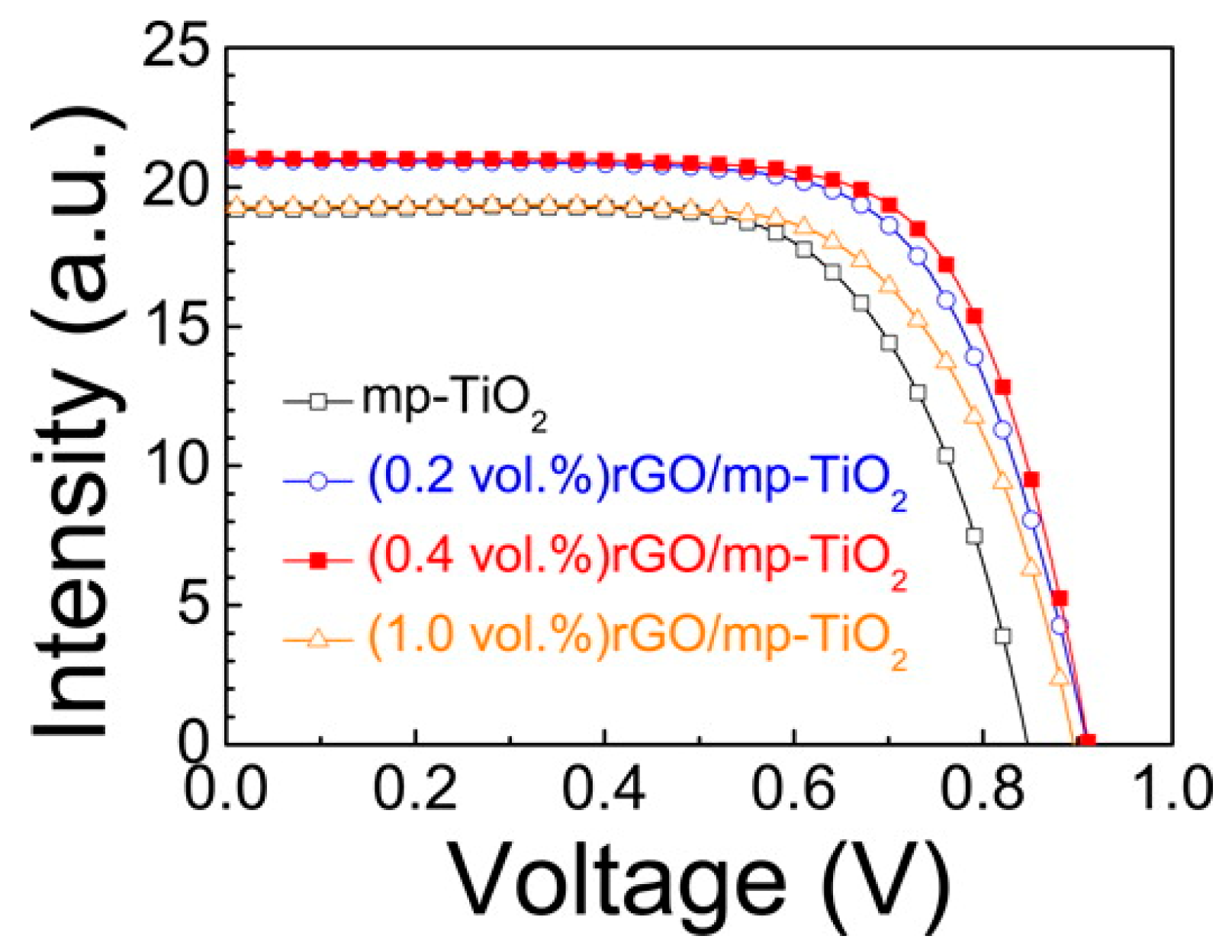
Also, GO and r-GO were investigated to boost the efficiency of PSCs. The r-GO synthesized by Hummers’ method was mixed with TiO2 slurry to form the final mixture and spin coated in a TiO2 blocking layer [62]. By altering the volume percentage of r-GO in the total ETL slurry, the r-GO concentration could be well modified, and, similarly, only a small portion of r-GO has a positive effect on the device performance. This is due to the r-GO light absorption in the visible light area. With an increased amount of r-GO, the incident light that was acquired by perovskite was reduced. Therefore, the Jsc was cut down. According to their results, the 0.4 vol % was the best ratio, with an efficiency of 14.5%, which was clearly higher than their TiO2-only device (11.5%). The corresponding J-V characteristics are shown in Figure 7. Another report using r-GO in both compact and mesoporous TiO2 also showed an increased efficiency with its reference cell. However, this work showed a lower efficiency of 9.3%, with an r-GO ratio of 0.15 wt % in compact TiO2 and 0.015 wt % in meso-TiO2 [63]. Besides the mixed slurry approach, the layer-by-layer method could be also effective and its experimental proof was reported in 2016 [64]. A modified Hummers’ method [59] was used for GO synthesis. Li doping was applied inside the re-dispersed GO solution, and the total mixture was re-dispersed by water/ethanol that was ready for spin coating under an inert atmosphere. By inserting this Li-doped GO layer, the Jsc and fill factor (FF) was boosted but the Voc had a slight decrease due to TiO2 conduction band edge shrinking (negative effect of Li doping). The efficiency of the GO-injected device was 11.8% and the reference cell was 10.3%. Moreover, the GO layer injection significantly reduced the J-V hysteresis. According to the investigators, it is believed that Li-GO layer could reduce the trap-assisted recombination at TiO2/perovskite interface. The addition of Li-GO layer also reduced the device decay rate in the initial stage, but has no clear improvement for the long-term device stability.
3.3.3. Graphene and Graphene Oxide in HTL
Research on using graphene-related films as HTL also attracts great attention. Wu et al. [65] spin-coated GO films that were prepared from a modified Hummer’s method, as described in a previous protocol [66], on ITO substrate as the HTL. The perovskite film grown on GO showed better film coverage and larger crystal size than typical PEDOT:PSS and bare ITO. Also, a strong preferential growth in (110) plane was observed for perovskite on GO layer, indicating high carrier mobility in perovskite films. Thus, the carrier separation and Jsc could be enhanced. The inverted PSC with GO as the HTL achieved a high PCE of 12.40%, as shown in Figure 8, while the one with PEDOT:PSS showed only 9.26%. They also suggested that a higher GO suspension concentration and thicker GO film could have a better enhancement with perovskite, and, hence, increased device efficiency.
Different attempts were made to accomplish this new HTL. The performance of r-GO was compared with the most typical Spiro-OMeTAD as the hole-transport layer [67]. The GO layer was spray-coated under N2 atmosphere on a pre-heated perovskite layer. In addition, the reference samples had either a spin-coated GO layer from the same GO suspension or a Spiro-OMeTAD layer. After evaporating the top Au grid, the J-V characteristics of PSCs showed that the Spiro-OMeTAD had a greater device efficiency due to both kinds of GO layers, and very little statistical difference could be found between the device efficiency of spin-coated and sprayed GO-based PSCs. However, due to a low stability of Spiro-OMeTAD, the efficiency of PSCs with Spiro-OMeTAD suffered a 41% loss after 1987 h. In the meantime, PSCs with GO showed a significantly good stability, and their efficiency increased from 4.87% to 6.62%, which was a 36% efficiency improvement due to better prevention on photo-generated carrier recombination at GO layer than Spiro-OMeTAD [68]. Detailed comparison on device stability could be found in Table 3.
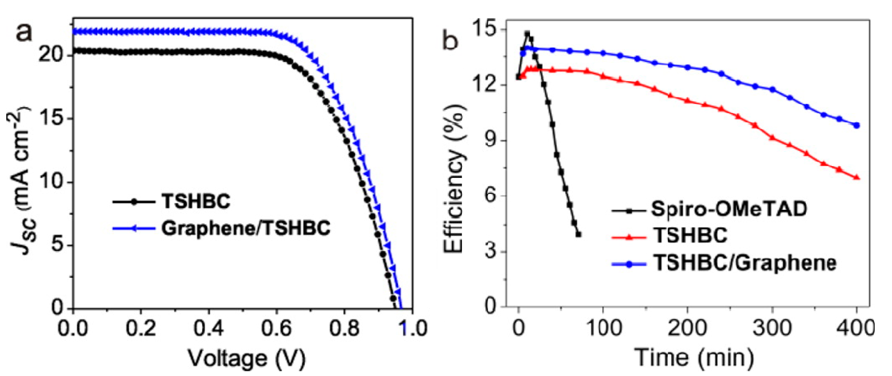
A similar comparison was also observed by Cao et al. [69]. Moreover, the initial device efficiency was also greatly improved in this work: A functionalized nano-graphene hole-transport material (perthiolated trisulfur-annulated hexa-peri-hexabenzocoronene, TSHBC) was applied. The thiol group, according to them, could be a strong binder between perovskite and graphene. Therefore, the hole-transportation rate would be accelerated. They reported an efficiency of 12.81% with a device structure of FTO/TiO2/CH3NH3PbI3/TSHBC/Au. Moreover, due to a better chemical stability of graphene, the fabrication process was finished in the air with 45% humidity, which was a bad condition for Spiro-OMeTAD fabrication. This group further improved their device efficiency up to 14% with introducing extra graphene sheets into TSHBC layer to improve its hole transportation phenomenon. Also, with a higher water contact angle of TSHBC/graphene than Spiro-OMeTAD, the 14% PSCs could gain a better moisture-resistance, which could also extend the device lifetime as shown in Figure 9. Another work from Hong Kong provided a detailed measurement of the hole extraction rate in both single and multilayer graphene hole transport layer, which was 3.7 and 5.1 ns−1, respectively [70]. Their best cell reached an efficiency of 11.5% with the help of multilayer graphene. The graphene HTL, according to their results, formed a Schottky barrier at the perovskite/graphene interface. Thus, the hole extraction and transportation processes could be enhanced while electrons could be blocked and recombination rate was decreased as well.
The investigations were conducted not only on the single graphene/GO HTL but also on the graphene/GO-composited HTL. In 2013, Luo et al. [71] claimed a 13.01% PSC using iodide-reduced GO together with Spiro-OMeTAD as the HTL. After initial GO preparation from both Hummer’s and Offeman’s method, the GO suspension was mixed with the self-prepared FeI2 solution and reduced by HCl. The r-GO and Spiro-OMeTAD were sequentially spin-coated on perovskite. Since r-GO and Spiro-OMeTAD have different energy levels, holes generated in perovskite could flow into either of them. Reduced GO could also extract holes from lower-level Spiro-OMeTAD and bring them to Au contact. Thus, this combined HTL works more efficient than either of them. Also, the existence of r-GO greatly improved the wettability and stability of PSCs. Another composited HTL, GO/PEDOT:PSS, brought an efficiency of 9.7% while the PSCs with PEDOT:PSS and GO showed only 8.2% and 6.4%, respectively [72]. The composited HTL led to the highest shunt resistance (Rsh) and lowest sheet resistance (Rs). The addition of graphene improved the device stability compared with bare PEDOT:PSS. In turns, PEDOT:PSS improved the surface coverage of ultrathin graphene.
3.3.4. Graphene as Contacts
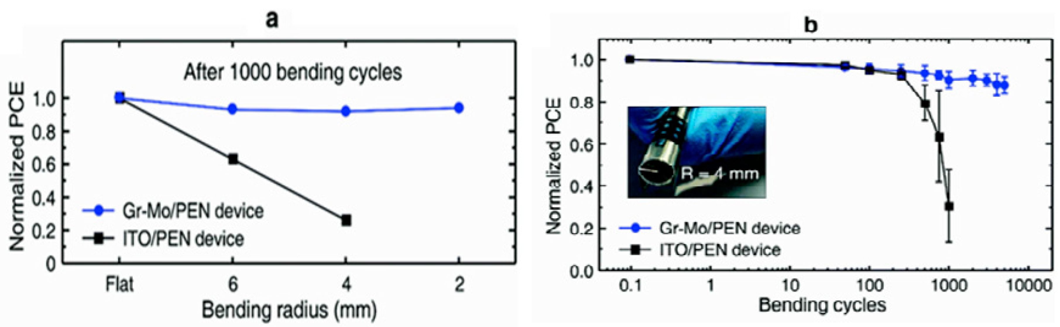
Although application of graphene in ETL and HTL was the primary focus, graphene could also be served as the electrodes of PSCs due to controllable conductivity, great carrier mobility and transparency. PSCs equipped with graphene electrode could be able to accept light from both sides. As reported by You et al. [73], the CVD-synthesized graphene was transferred with PMMA on a thin layer of PEDOT:PSS, which helped to modify the conductivity of thin-layer graphene electrodes. Graphene accumulation would also decrease the sheet resistance but the transparency would be also decreased. Their best PSC was with 2-layer graphene electrodes and showed an efficiency of 12.02% and 11.65% with illumination from FTO and graphene sides, respectively. Sung et al. [74] fabricated graphene on an inverted PSC with similar conductivity assistance. But they inserted a thin MoO3 layer between graphene and PEDOT:PSS due to better wettability of PEDOT:PSS on graphene/MoO3 shown in Figure 10. The device characterization showed 2 nm MoO3 layer had an improvement for both graphene and ITO electrodes: The best graphene-based PSCs showed an efficiency change from 12.1% to 17.1%, while the best ITO-based devices showed 17.6% and 18.8%, respectively. Table 4 showed device parameters for all PSCs. Detail characterization showed the MoO3-composited graphene had a higher work function of 4.71 eV. Also, the graphene sheet resistance dropped down by 5 folds with 2 nm MoO3. These results explained the clear efficiency change. Recently, Yoon et al. [75] fabricated a flexible PSC by using similar electrode design. The PSC had an inverted configuration with the best efficiency of 16.8%, while the flexible ITO electrode acquired 17.3%. However, after 1000 bending cycles, the ITO-based PSCs showed drastic efficiency decrease while the graphene-based PSCs suffered only minor change. Compared with ITO or other metal electrode, graphene electrodes occurred no crack after long-term bending, which showed great potential in flexible PSCs’ fabrication. The detailed comparison could be found in Figure 11.
3.3.5. Other Applications of Graphene in PSCs
In addition, graphene could also be mixed with perovskite slurry before depositing the adsorption layer. Hadadian et al. [76] applied an N-doped r-GO into perovskite slurry and they found an increase of perovskite grain size due to a slower crystallization. The graphene incorporation also brought surface passivation at perovskite/Spiro-OMeTAD interface due to the excellent carrier separation capability of graphene. Their best device had an efficiency of 18.7%, which is by far the best performance among all the graphene-based PSCs. Also, by combining the advantage of graphene at both ETL and HTL, one group acquired an efficiency of 18.2%, which was already close to those top-tier PSCs [77]. However, the 16 h illumination test revealed nearly 70% efficiency loss and a further 1000 h shelf-life condition test displayed about 45% efficiency loss, indicating the graphene-composited interface may not be as stable as predicted.
Overall, graphene has been demonstrated with sufficient space in PSCs. With the proper enhancement of conductivity and surface compatibility, graphene could bring PSCs to the next stage. The soft nature of graphene also provides possibility to produce flexible PSCs, which could be identical to large-scale and roll-to-roll production.
4. Applications and Future Research
The above research indicates that the graphene can be used for enhancing the performance of solar cells in various ways. Firstly, graphene can be used in top and back contacts of CdTe solar cells due to its work function matching with CdTe and a better carrier mobility. However, the top contact needs 1–5 layers of graphene in order to minimize the optical absorptions. Due to the zero bandgap of graphene, a schottky junction would be formed between graphene and CdTe, however; no evidence supports that this kind of junction improves carrier separation process. Similarly, graphene is also applied in graphene-composited CIGS or CZTS system (to replace AZO and/or combine with Mo or other metal contacts) but additional efforts could be made on reducing the contact resistance between graphene and other components (i-ZnO, top grid and/or absorber) in CIGS and CZTS based cells. In PSCs, graphene could be applied in every component: in ETL, graphene was initially mixed with TiO2 but Li-GO/TiO2 double-layer structure was also proved successful. Bu considering the advantage of graphene over FTO, a new ETL/contact structure with graphene and graphene-incorporated ETL might be considered, however; graphene concentration should be maintained at a low level. In HTL fabrication, graphene/GO could be used as HTL by itself or mixed with some typical hole-transport materials. However, the key is to find an efficient structural and electrical binder between graphene/GO and perovskite otherwise the PEC may not be improved. Such binder is also important with graphene front/back contacts in PSCs. In addition, more work could be focused on introducing graphene into perovskite layer due to possibly better perovskite crystal formation, which is vital to improve device efficiency and durability. Table 5 summarizes the key fields towards to those findings and suggestions. Authors expect more investigations will be performed in CZTS-based solar cells in the future.
Since the solar cells are large-area devices, process scalability is very important for a commercial viability of usage of graphene in solar cells. In particular, the top contacts need 1–5 layers of graphene and it is a challenging process to manufacture such materials in large-scale. Also, one of the primary reasons for degradation of PSCs is the heating effect, which produces photo-inactive phase in perovskite layer. Since graphene is one of the highest thermal conductive materials, the heating effect can be significantly controlled by an appropriate level of incorporation of graphene. These research can be very useful steps towards increasing the durability of PSCs. Many investigations indicated that the pristine graphene can be used in solar cells. However, further improvements of conversion efficiency might be possible with functionalized graphene. Therefore, investigations related to the application of functionalized graphene in the solar cells can be very useful in both fundamental and application viewpoints. Also, further investigations are important to understand the application of graphene as front and back contacts of flexible and semitransparent solar cell system.
5. Conclusions
Graphene, with its extremely high carrier mobility and transparency together with suitable work function, had been proved as a suitable replacement of the TCO layer for CdTe and CIGS system. The graphene front contacts could have a mono-layer structure but the back contacts should have adequate thickness to prevent extra current loss. However, the experiment indicated that the graphene layer itself tends to suffer incomplete surface coverage and a higher sheet resistance in a lateral direction, which leads to a current leakage and insufficient carrier transportation. Suitable metallic doping could improve the performance of device. In order to have advantage of band structure, the controllability of number of layers in a graphene manufacturing should be optimized.
For the perovskite solar cells (PSCs), a positive effect has also been demonstrated by application of graphene in almost every component. Compared with the conventional design, the usage of graphene enhanced the carrier extraction and device stability (compared with Spiro-OMeTAD). The flexible devices is also achieved by the fabrication of printable graphene-based PSCs on a soft substrate. Also, the preliminary test showed such flexible cells were durable after a large amount of bending cycles. Moreover, the application of graphene in multiple positions already showed a higher efficiency than PSC without graphene. However, the feasibility studies are necessary to integrate graphene usage in the solar cell manufacturing processes. The application of r-GO in PSCs was also briefly discussed. Although the long-term stability test showed the advantage of graphene over the conventional HTL, the loss of device parameters should be addressed before the commercialization stage.
Acknowledgments
One of the authors, Zhengqi Shi, would like to acknowledge the financial assistance given by the University of Toledo for this study.
Author Contributions
Both authors have analyzed the literature and prepared this manuscript.
Conflicts of Interest
The authors declare no conflict of interest.
References
- Novoselov, K.S.; Geim, A.K.; Morozov, S.V.; Jiang, D.; Katsnelson, M.I.; Grigorieva, I.V.; Dubonos, S.V.; Firsov, A.A. Two-dimensional gas of massless Dirac fermions in graphene. Nature 2005, 438, 197–200. [Google Scholar] [CrossRef] [PubMed] [Green Version]
- Lee, C.; Wei, X.; Kysar, J.W.; Hone, J. Measurement of the elastic properties and intrinsic strength of monolayer grapheme. Science 2008, 321, 385–388. [Google Scholar] [CrossRef] [PubMed]
- Bolotin, K.I.; Sikes, K.J.; Jiang, Z.; Klima, M.; Fudenberg, G.; Hone, J.; Kim, P.; Stormer, H.L. Ultrahigh electron mobility in suspended grapheme. Solid State Commun. 2008, 146, 351–355. [Google Scholar] [CrossRef]
- Nair, R.R.; Blake, P.; Grigorenko, A.N.; Novoselov, K.S.; Booth, T.J.; Stauber, T.; Peres, N.M.R.; Geim, A.K. Fine structure constant defines visual transparency of grapheme. Science 2008, 20, 1308. [Google Scholar] [CrossRef] [PubMed]
- Balandin, A.A.; Ghosh, S.; Bao, W.; Calizo, I.; Teweldebrhan, D.; Miao, F.; Lau, C.N. Superior thermal conductivity of single-layer grapheme. Nano Lett. 2008, 8, 902–907. [Google Scholar] [CrossRef] [PubMed]
- Ganz, E.; Ganz, A.B.; Yang, L.; Dornfeld, M. The initial stages of melting of graphene between 4000 K and 6000 K. Phys. Chem. Chem. Phys. 2017, 19, 3756–3762. [Google Scholar] [CrossRef] [PubMed]
- Gautam, M.; Jayatissa, A.H. Gas sensing properties of graphene synthesized by chemical vapor deposition. Mater. Sci. Eng. C 2011, 31, 1405–1411. [Google Scholar] [CrossRef]
- Gautam, M.; Jayatissa, A.H. Ammonia gas sensing behavior of graphene surface decorated with gold nanoparticles. Solid State Electron. 2012, 78, 159–165. [Google Scholar] [CrossRef]
- Park, D.W.; Schendel, A.A.; Mikael, S.; Brodnick, S.K.; Richner, T.J.; Ness, J.P.; Hayat, M.R.; Atry, F.; Frye, S.T.; Pashaie, R.; et al. Graphene-based carbon-layered electrode array technology for neural imaging and optogenetic applications. Nat. Commun. 2014, 5, 5258. [Google Scholar] [CrossRef] [PubMed]
- Yu, T.; Wang, F.; Xu, Y.; Ma, L.; Pi, X.; Yang, D. Graphene coupled with silicon quantum dots for high-performance bulk-silicon-based Schottky-junction photodetectors. Adv. Mater. 2016, 28, 4912–4919. [Google Scholar] [CrossRef] [PubMed]
- Narayanan, R.; Yamada, H.; Karakaya, M.; Podila, R.; Rao, A.M.; Bandaru, P.R. Modulation of the electrostatic and quantum capacitances of few layered graphenes through plasma processing. Nano Lett. 2015, 15, 3067–3072. [Google Scholar] [CrossRef] [PubMed]
- De Arco, L.G.; Zhang, Y.; Schlenker, C.W.; Ryu, K.; Thompson, M.E.; Zhou, C. Continuous, highly flexible, and transparent graphene films by chemical vapor deposition for organic photovoltaics. ACS Nano 2010, 4, 2865–2873. [Google Scholar] [CrossRef] [PubMed]
- Novoselov, K.S.; Geim, A.K.; Morozov, S.V.; Jiang, D.; Zhang, Y.; Dubonos, S.V.; Grigorieva, I.V.; Firsov, A.A. Electric field effect in atomically thin carbon films. Science 2004, 306, 666–669. [Google Scholar] [CrossRef] [PubMed]
- Rafiee, J.; Mi, X.; Gullapalli, H.; Thomas, A.V.; Yavari, F.; Shi, Y.; Ajayan, P.M.; Koratkar, N.A. Wetting transparency of grapheme. Nat. Mater. 2012, 11, 217–222. [Google Scholar] [CrossRef] [PubMed]
- Das, S.; Drucker, J. Nucleation and growth of single layer graphene on electrodeposited Cu by cold wall chemical vapor deposition. Nanotechnology 2017, 28, 105601. [Google Scholar] [CrossRef] [PubMed]
- Kim, D.Y.; Sinha-Ray, S.; Park, J.J.; Lee, J.G.; Cha, Y.H.; Bae, S.H.; Ahn, J.H.; Jung, Y.C.; Kim, S.M.; Yarin, A.L.; et al. Self-healing reduced graphene oxide films by supersonic kinetic spraying. Adv. Funct. Mater. 2014, 24, 4986–4995. [Google Scholar] [CrossRef]
- Lin, J.; Peng, Z.; Liu, Y.; Ruiz-Zepeda, F.; Ye, R.; Samuel, E.L.G.; Yacaman, M.J.; Yakoboson, B.I.; Tour, J.M. Laser-induced porous graphene films from commercial polymers. Nat. Commun. 2014, 5, 5714. [Google Scholar] [CrossRef] [PubMed]
- Hummers, W.S.; Offeman, R.E. Preparation of graphite oxide. J. Am. Chem. Soc. 1958, 80, 1339. [Google Scholar] [CrossRef]
- Gautam, M.; Shi, Z.; Jayatissa, A.H. Graphene films as transparent electrodes for photovoltaic devices based on cadmium sulfide thin films. Solar Energy Mater. Solar Cells 2017, 163, 1–8. [Google Scholar] [CrossRef]
- Becker, J.J.; Boccard, M.; Campbell, C.M.; Zhao, Y.; Lassise, M.; Holman, Z.C.; Zhang, Y. Loss analysis of monocrystalline CdTe solar cells with 20% active-area efficiency. IEEE J. Photovolt. 2017, 7, 900–905. [Google Scholar] [CrossRef]
- Kato, T.; Honda, A.; Yagioka, T.; Matsuura, T.; Yamamoto, K.; Higashi, S.; Wu, J.L.; Tai, K.F.; Hiroi, H.; Yoshiyama, T.; et al. Enhanced efficiency of Cd-free Cu(In, Ga)(Se, S)2 minimodule via (Zn, Mg)O second buffer layer and alkali post treatment. IEEE J. Photovolt. 2017, 7, 1773–1780. [Google Scholar] [CrossRef]
- Shi, Z.; Attygalle, D.; Jayatissa, A.H. Kesterite-based next generation high performance thin film solar cell: Current progress and future prospects. J. Mater. Sci. Mater. Electron. 2017, 28, 2290–2306. [Google Scholar] [CrossRef]
- Shi, Z.; Jayatissa, A.H. One-pot hydrothermal synthesis and fabrication of kesterite Cu2ZnSn(S, Se)4 thin films. Prog. Nat. Sci. Mater. Int. 2017, 27, 550–555. [Google Scholar] [CrossRef]
- Yang, W.S.; Park, B.W.; Jung, E.H.; Jeon, N.J.; Kim, Y.C.; Lee, D.U.; Shin, S.S.; Seo, J.; Kim, E.K.; Noh, J.H.; et al. Iodide management in formamidinium-lead-halide-based perovskite layers for efficient solar cells. Science 2017, 356, 1376–1379. [Google Scholar] [CrossRef] [PubMed]
- Arora, N.; Dar, M.I.; Hinderhofer, A.; Pellet, N.; Schreiber, F.; Grätzel, S.M.Z.M. Perovskite solar cells with CuSCN hole extraction layers yield stabilized efficiencies greater than 20%. Science 2017. [Google Scholar] [CrossRef] [PubMed]
- Shi, Z.; Jayatissa, A.H.; Peiris, F.C. Fabrication of semiconducting pyrite thin films from hydrothermally synthesized pyrite (FeS2) powder. J. Mater. Sci. Mater. Electron. 2016, 27, 535–542. [Google Scholar] [CrossRef]
- Shockley, W.; Queisser, H.J. Detailed balance limit of efficiency of p-n junction solar cells. J. Appl. Phys. 1961, 32, 510–519. [Google Scholar] [CrossRef]
- Oh, J.S.; Kim, K.N.; Yeom, G.Y. Graphene doping methods and device applications. J. Nanosci. Nanotechnol. 2014, 14, 1120–1133. [Google Scholar] [CrossRef] [PubMed]
- Yu, Y.J.; Zhao, Y.; Ryu, S.; Brus, L.E.; Kim, K.S.; Kim, P. Tuning the graphene work function by electric field effect. Nano Lett. 2009, 9, 3430–3434. [Google Scholar] [CrossRef] [PubMed]
- Parui, S.; Ruiter, R.; Zomer, P.J.; Wojtaszek, M.; van Wees, B.J.; Banerjee, T. Temperature dependent transport characteristics of graphene/n-Si diodes. J. Appl. Phys. 2014, 116, 244505. [Google Scholar] [CrossRef]
- An, Y.; Behnam, A.; Pop, E.; Ural, A. Metal-semiconductor-metal photodetectors based on graphene/p-type silicon Schottky junctions. Appl. Phys. Lett. 2013, 102, 013110. [Google Scholar] [CrossRef]
- Tongay, S.; Lemaitre, M.; Miao, X.; Gila, B.; Appleton, B.R.; Hebard, A.F. Rectification at graphene-semiconductor interfaces: Zero-gap semiconductor-based diodes. Phys. Rev. X 2012, 2, 011002. [Google Scholar] [CrossRef]
- Sonde, S.; Giannazzo, F.; Raineri, V.; Yakimova, R.; Huntzinger, J.R.; Tiberj, A.; Camassel, J. Electrical properties of the graphene/4H-SiC (0001) interface probed by scanning current spectroscopy. Phys. Rev. B 2009, 80, 241406. [Google Scholar] [CrossRef]
- Tongay, S.; Schumann, T.; Hebard, A.F. Graphite based Schottky diodes formed on Si, GaAs, and 4H-SiC substrates. Appl. Phys. Lett. 2009, 95, 222103. [Google Scholar] [CrossRef]
- Wang, J.; Deng, S.; Liu, Z.; Liu, Z. The Rare Two-Dimensional Materials with Dirac Cones. arXiv 2015, arXiv:1410.5895. [Google Scholar]
- Riazimehr, S.; Bablich, A.; Schneider, D.; Kataria, S.R.; Passi, V.; Yim, C.; Duesberg, G.S.; Lemme, M.C. Spectral sensitivity of graphene/silicon heterojunction photodetectors. arXiv 2016, arXiv:1509.01021. [Google Scholar]
- Bi, H.; Huang, F.; Liang, J.; Xie, X.; Jiang, M. Transparent conductive graphene films synthesized by ambient pressure chemical vapor deposition used as the front electrode of CdTe solar cells. Adv. Mater. 2011, 23, 3202–3206. [Google Scholar] [CrossRef] [PubMed]
- Yang, N.; Zhai, J.; Wang, D.; Chen, Y.; Jiang, L. Two-dimensional graphene bridges enhanced photoinduced charge transport in dye-sensitized solar cells. ACS Nano 2010, 4, 887–894. [Google Scholar] [CrossRef] [PubMed]
- Bi, H.; Huang, F.; Liang, J.; Tang, Y.; Lv, X.; Xie, X.; Jiang, M. Large-scale preparation of highly conductive three dimensional graphene and its applications in CdTe solar cells. J. Mater. Chem. 2011, 21, 17366–17370. [Google Scholar] [CrossRef]
- Liang, J.; Bi, H.; Wan, D.; Huang, F. Novel Cu nanowires/graphene as the back contact for CdTe solar cells. Adv. Funct. Mater. 2012, 22, 1267–1271. [Google Scholar] [CrossRef]
- Lin, T.; Huang, F.; Liang, J.; Wang, Y. A facile preparation route for boron-doped graphene, and its CdTe solar cell application. Energy Environ. Sci. 2011, 4, 862–865. [Google Scholar] [CrossRef]
- Brus, V.V.; Maryanchuk, P.D.; Ilashchuk, M.I.; Rappich, J.; Babichuk, I.S.; Kovalyuk, Z.D. Graphitic carbon/n-CdTe Schottky-type heterojunction solar cells prepared by electron-beam evaporation. Sol. Energy 2015, 112, 78–84. [Google Scholar] [CrossRef]
- Lin, S.; Li, X.; Zhang, S.; Wang, P.; Xu, Z.; Zhong, H.; Wu, Z.; Chen, H. Graphene/CdTe heterostructure solar cell and its enhancement with photo-induced doping. Appl. Phys. Lett. 2015, 107, 191106. [Google Scholar] [CrossRef]
- Aldosari, M.; Sohrabpoor, H.; Gorji, N.E. Optical modeling of graphene contacted CdTe solar cells. Superlattices Microstruct. 2016, 92, 242–248. [Google Scholar] [CrossRef]
- Housemand, M.; Zandi, M.H.; Gorji, N.E. SCAPS modeling for degradation of ultrathin CdTe Films: Materials interdiffusion. J. Miner. Met. Mater. Soc. 2015, 67, 2062–2070. [Google Scholar] [CrossRef]
- Okamoto, T.; Hayashi, R.; Ogawa, Y.; Hosono, A.; Doi, M. Fabrication of polycrystalline CdTe thin-film solar cells using carbon electrodes with carbon nanotubes. Jpn. J. Appl. Phys. 2015, 54, 04DR01. [Google Scholar] [CrossRef]
- Kuhn, L.; Gorji, N.E. Review on the graphene/nanotube application in thin film solar cells. Mater. Lett. 2016, 171, 323–326. [Google Scholar] [CrossRef]
- Yin, E.; Zhang, K.; Luo, H.; Cheng, G.; Ma, X.; Xiong, Z.; Xiao, X. Highly efficient graphene-based Cu(In, Ga)Se2 solar cells with large active area. Nanoscale 2014, 6, 10879–10886. [Google Scholar] [CrossRef] [PubMed]
- Dissanayake, D.M.N.M.; Ashraf, A.; Dwyer, D.; Kisslinger, K.; Zhang, L.; Pang, Y.; Efstathiadis, H.; Eisaman, M.D. Spontaneous and strong multi-layer graphene n-doping on soda-lime glass and its application in graphene-semiconductor junctions. Sci. Rep. 2016, 6, 21070. [Google Scholar] [CrossRef] [PubMed]
- Houshmand, M.; Zandi, M.H. Modeling of optical losses in graphene contacted CIGS solar cells. Mod. Phys. Lett. B 2016, 30, 1650342. [Google Scholar] [CrossRef]
- Nikita, K.N.; Gaffar, M.A.; Chowdhury, M.I.B. Exploring the opportunity of using graphene as the transparent conducting layer in CZTS-based thin film solar cells. In Proceedings of the 3rd International Conference on Electrical Engineering and Information Communication Technology (ICEEICT), Dhaka, Bangladesh, 22–24 September 2016; pp. 1–6. [Google Scholar]
- Ishikawa, R.; Oya, T.; Yamada, T.; Nomoto, T.; Tsuboi, N. Highly oriented CuInS2 thin films on graphene electrodes for solar-cell applications. Thin Solid Films 2017, 634, 1–5. [Google Scholar] [CrossRef]
- Kamalanathan, M.; Karuppusamy, S.; Sivakumar, R.; Gopalakrishnan, R. Synthesis of reduced graphene oxide-copper tin sulphide composites and their photoconductivity enhancement for photovoltaic applications. J. Mater. Sci. 2015, 50, 8029–8037. [Google Scholar] [CrossRef]
- Saliba, M.; Matsui, T.; Seo, J.Y.; Domanski, K.; Correa-Baena, J.P.; Nazeeruddin, M.K.; Zakeeruddin, S.M.; Tress, W.; Abate, A.; Hagfeldt, A.; et al. Cesium-containing triple cation perovskite solar cells: Improved stability, reproducibility and high efficiency. Energy Environ. Sci. 2016, 9, 1989–1997. [Google Scholar] [CrossRef] [PubMed]
- Jeon, N.J.; Noh, J.H.; Yang, W.S.; Kim, Y.C.; Ryu, S.; Seo, J.; Seok, S.I. Compositional engineering of perovskite materials for high-performance solar cells. Nature 2015, 517, 476–480. [Google Scholar] [CrossRef] [PubMed]
- Lee, M.M.; Teuscher, J.; Miyasaka, T.; Murakami, T.N.; Snaith, H.J. Efficient hybrid solar cells based on meso-superstructured organometal halide perovskites. Science 2012, 338, 643–647. [Google Scholar] [CrossRef] [PubMed]
- Anaraki, E.H.; Kermanpur, A.; Steier, L.; Domanski, K.; Matsui, T.; Tress, W.; Saliba, M.; Abate, A.; Gratzel, M.; Hagfeldt, A.; et al. Highly efficient and stable planar perovskite solar cells by solution-processed tin oxide. Energy Environ. Sci. 2016, 9, 3128–3134. [Google Scholar] [CrossRef]
- Saliba, M.; Matsui, T.; Domanski, K.; Seo, J.-Y.; Ummadisingu, A.; Zakeeruddin, S.M.; Correa-Baena, J.P.; Tress, W.R.; Abate, A.; Hagfeldt, A.; et al. Incorporation of rubidium cations into perovskite solar cells improves photovoltaic performance. Science 2016, 354, 206–209. [Google Scholar] [CrossRef] [PubMed]
- Wang, J.T.W.; Ball, J.M.; Barea, E.M.; Abate, A.; Webber, J.A.A.; Huang, J.; Saliba, M.; Mora-Sero, I.; Bisquert, J.; Snaith, H.J.; et al. Low-temperature processed electron collection layers of graphene/TiO2 nanocomposites in thin film perovskite solar cells. Nano Lett. 2014, 14, 724–730. [Google Scholar] [CrossRef] [PubMed]
- Zhu, Z.; Ma, J.; Wang, Z.; Mu, C.; Fan, Z.; Du, L.; Bai, Y.; Fan, L.; Yan, H.; Phillips, D.L.; et al. Efficiency enhancement of perovskite solar cells through fast electron extraction: The role of graphene quantum dots. J. Am. Chem. Soc. 2014, 136, 3760–3763. [Google Scholar] [CrossRef] [PubMed]
- Han, G.S.; Song, Y.H.; Jin, Y.U.; Lee, J.W.; Park, N.G.; Kang, B.K.; Lee, J.K.; Cho, I.S.; Yoon, D.H.; Jung, H.S. Reduced graphene oxide/mesoporous TiO2 nanocomposite based perovskite solar cells. ACS Appl. Mater. Interfaces 2015, 7, 23521–23526. [Google Scholar] [CrossRef] [PubMed]
- Tomokazu, U.; Daichi, M.; Jinseok, B.; Satyajit, G.; Seigo, I.; Vaidyanathan (Ravi), S.; Hiroshi, I. Boosting of the performance of perovskite solar cells through systematic introduction of reduced graphene oxide in TiO2 layers. Chem. Lett. 2015, 44, 1410–1412. [Google Scholar]
- Agresti, A.; Pescetelli, S.; Cinà, L.; Konios, D.; Kakavelakis, G.; Kymakis, E.; Carlo, A.D. Efficiency and stability enhancement in perovskite solar cells by inserting lithium-neutralized graphene oxide as electron transporting layer. Adv. Funct. Mater. 2016, 26, 2686–2694. [Google Scholar] [CrossRef]
- Poh, H.L.; Šanek, F.; Ambrosi, A.; Zhao, G.; Sofer, Z.; Pumera, M. Graphenes prepared by Staudenmaier, Hofmann and Hummers methods with consequent thermal exfoliation exhibit very different electrochemical properties. Nanoscale 2012, 4, 3515–3522. [Google Scholar] [CrossRef] [PubMed]
- Wu, Z.; Bai, S.; Xiang, J.; Yuan, Z.; Yang, Y.; Cui, W.; Gao, X.; Liu, Z.; Jin, Y.; Sun, B. Efficient planar heterojunction perovskite solar cells employing graphene oxide as hole conductor. Nanoscale 2014, 6, 10505–10510. [Google Scholar] [CrossRef] [PubMed]
- Liu, Z.; Robinson, J.T.; Sun, X.; Dai, H. PEGylated nanographene oxide for delivery of water-insoluble cancer drugs. J. Am. Chem. Soc. 2008, 130, 10876–10877. [Google Scholar] [CrossRef] [PubMed]
- Yun, J.-M.; Yeo, J.-S.; Kim, J.; Jeong, H.-G.; Kim, D.-Y.; Noh, Y.J.; Kim, S.-S.; Ku, B.-C.; Na, S.-I. Solution-processable reduced graphene oxide as a novel alternative to PEDOT:PSS hole transport layers for highly efficient and stable polymer solar cells. Adv. Mater. 2011, 23, 4923–4928. [Google Scholar] [CrossRef] [PubMed]
- Palma, A.L.; Cinà, L.; Pescetelli, S.; Agresti, A.; Raggio, M.; Paolesse, R.; Bonaccorso, F.; Carlo, A.D. Reduced graphene oxide as efficient and stable hole transporting material in mesoscopic perovskite solar cells. Nano Energy 2016, 22, 349–360. [Google Scholar] [CrossRef]
- Cao, J.; Liu, Y.-M.; Jing, X.; Yin, J.; Li, J.; Xu, B.; Tan, Y.-Z.; Zheng, N. Well-Defined thiolated nanographene as hole-transporting material for efficient and stable perovskite solar cells. J. Am. Chem. Soc. 2015, 137, 10914–10917. [Google Scholar] [CrossRef] [PubMed]
- Yan, K.; Wei, Z.; Li, J.; Chen, H.; Yi, Y.; Zheng, X.; Long, X.; Wang, Z.; Wang, J.; Xu, J.; et al. High-performance graphene-based hole conductor-free perovskite solar cells: Schottky junction enhanced hole extraction and electron blocking. Small 2015, 11, 2269–2274. [Google Scholar] [CrossRef] [PubMed]
- Luo, Q.; Zhang, Y.; Liu, C.; Li, J.; Wang, N.; Lin, H. Iodide-reduced graphene oxide with dopant-free spiro-OMeTAD for ambient stable and high-efficiency perovskite solar cells. J. Mater. Chem. A 2015, 3, 15996–16004. [Google Scholar] [CrossRef]
- Lee, D.-Y.; Na, S.-I.; Kim, S.-S. Graphene oxide/PEDOT:PSS composite hole transport layer for efficient and stable planar heterojunction perovskite solar cells. Nanoscale 2016, 8, 1513–1522. [Google Scholar] [CrossRef] [PubMed]
- You, P.; Liu, Z.; Tai, Q.; Liu, S.; Yan, F. Efficient semitransparent perovskite solar cells with graphene electrodes. Adv. Mater. 2015, 27, 3632–3638. [Google Scholar] [CrossRef] [PubMed]
- Sung, H.; Ahn, N.; Jang, M.S.; Lee, J.-K.; Yoon, H.; Park, N.-G.; Choi, M. Transparent conductive oxide-free graphene-based perovskite solar cells with over 17% efficiency. Adv. Energy Mater. 2016, 6, 1501873. [Google Scholar] [CrossRef]
- Yoon, J.; Sung, H.; Lee, G.; Cho, W.; Ahn, N.; Jung, H.S.; Choi, M. Superflexible, high-efficiency perovskite solar cells utilizing graphene electrodes: Towards future foldable power sources. Energy Environ. Sci. 2017, 10, 337–345. [Google Scholar] [CrossRef]
- Hadadian, M.; Correa-Baena, J.-P.; Goharshadi, E.K.; Ummadisingu, A.; Seo, J.-Y.; Luo, J.; Gholipour, S.; Zakeeruddin, S.M.; Saliba, M.; Abate, A.; et al. Enhancing efficiency of perovskite solar cells via n-doped graphene: Crystal modification and surface passivation. Adv. Mater. 2016, 28, 8681–8686. [Google Scholar] [CrossRef] [PubMed]
- Agresti, A.; Pescetelli, S.; Taheri, B.; Castillo, A.E.D.R.; Cinà, L.; Bonaccorso, F.; Carlo, A.D. Graphene-perovskite solar cells exceed 18% efficiency: A stability study. ChemSusChem 2016, 9, 2609–2619. [Google Scholar] [CrossRef] [PubMed]
Figure 1.
(a) Atomic structure and (b) energy bands of graphene. The energy bands have been calculated by first-principles (black line) and the tight-binding models: green lines indicate calculation assuming (E0 = 0) and red lines indicate cone-like band structure with linear dispersion near Dirac points K and K’ [35].

Figure 2.
J-V plot of the graphene/n-Si diode on (a) linear and (b) semi-logarithmic scale in the dark and under illumination; (c) the graphene/n-Si interface at zero bias voltage. EC, EV, EF, Eg, WG, χSi and Φb indicate conduction band, valence band, Fermi level, bandgap, graphene work function, Si electron affinity and Schottky barrier height, respectively [36].

Figure 3.
(a) Scanning electron microscopy (SEM) of a graphene incorporated CdTe film, insert figure was the top-view. (b) A schematic draw of 3D graphene-incorporated CdTe solar cell. (c) Band structure of the CdTe solar cell with graphene back contact. (d) J–V curve of CdTe solar cell with graphene back contact [39].

Figure 4.
Current density versus voltage (J-V) characteristics of the graphene added devices with and without CdSe QDs under (a) AM1.5G illumination and (b) dark. The inset of (a) shows statistical results of devices with and without QDs. (c) External quantum efficiency (EQE) curves of the devices with and without CdSe QDs. (d) The absorption spectrum of the CdSe QDs [43].

Figure 5.
Schematic of multilayer arrangement in possible graphene-based CIGS device [48]. Graphene is incorporated at step-4 in all processes except standard process.
Figure 5.
Schematic of multilayer arrangement in possible graphene-based CIGS device [48]. Graphene is incorporated at step-4 in all processes except standard process.

Figure 6.
(a) Cross-sectional SEM image and (b) energy levels of the PSC with a graphene-TiO2 composite as the electron transport layer (ETL). (c) The series resistance of the perovskite solar cells (PSCs) with a graphene-TiO2 composite or TiO2 only as the ETL. (d) J-V characteristics of the PSCs with different electron collection layers under AM 1.5G and dark [60].

Figure 7.
J-V curve of rGO/ mesoporous-TiO2 nanocomposite based perovskite solar cell with varying rGO contents (0.2 vol %, 0.4 vol %, and 1.0 vol %). The black line stands for the reference cell with mesoporous-TiO2 nanolayers [62].
Figure 7.
J-V curve of rGO/ mesoporous-TiO2 nanocomposite based perovskite solar cell with varying rGO contents (0.2 vol %, 0.4 vol %, and 1.0 vol %). The black line stands for the reference cell with mesoporous-TiO2 nanolayers [62].

Figure 8.
(a) J–V characteristics and (b) EQE spectrum of the champion device with graphene/graphene oxide (GO) layer [65].
Figure 8.
(a) J–V characteristics and (b) EQE spectrum of the champion device with graphene/graphene oxide (GO) layer [65].

Figure 9.
(a) Best I−V curves of TSHBC (perthiolated trisulfur-annulated hexa-peri-hexabenzocoronene) and G/TSHBC-based cells and (b) Device stability test with AM1.5G under 45% humidity [69].
Figure 9.
(a) Best I−V curves of TSHBC (perthiolated trisulfur-annulated hexa-peri-hexabenzocoronene) and G/TSHBC-based cells and (b) Device stability test with AM1.5G under 45% humidity [69].

Figure 10.
PEDOT:PSS droplet contact angles on (a) as-prepared graphene, (b) graphene covered with 1 nm MoO3, (c) graphene covered with 2 nm MoO3, (d) as-prepared ITO, (e) UVO-treated ITO, (f) ITO covered with 1 nm MoO3 after UVO treatment. The insets in (a–c) showed the optical images of PEDOT:PSS/MAPbI3 films fabricated on the corresponding glass/graphene surfaces [74].

Figure 11.
(a) Normalized PCEs of the Gr-Mo/PEN and ITO/PEN devices measured after 1000 bending cycles with bending radius of flat, 6, 4, and 2 mm. (b) Normalized PCEs vs bending cycles at a bending radius of 4 mm for the Gr-Mo/PEN and ITO/PEN devices. The inset photograph shows the actual bending situation [75].


Table 1.
Device performances of the CdTe cells with four different back contacts [40]. This table contains conductivity (σ), carrier mobility (μ), open circuit voltage (Voc), short circuit current density (Jsc), fill factor (FF) and efficiency (Eff) for back contacts made with Cu thin films (Cu TFs) followed by a thick Ni layer, graphite or graphene paste containing Cu particles (Cu Ps, ≈75 μm in diameter) and copper nanowires (Cu NWs)/graphene.
| Back Contact Material | σ [S cm-1] | μ [cm2 V-1 s-1] | Voc [mV] | Jsc [mA cm-2] | FF [%] | Eff. [%] |
|---|---|---|---|---|---|---|
| Cu NWs/Graphene | 16.7 | 16.2 | 801 | 22.4 | 67.4 | 12.1 |
| Cu Ps/Graphene | 14.2 | 13.2 | 805 | 21.3 | 68.1 | 11.7 |
| Cu Ps/Graphite | 5.5 | 5.0 | 790 | 21.2 | 62.5 | 10.5 |
| Cu TF | - | - | 740 | 21.1 | 58.0 | 9.1 |
Table 2.
Graphene-composited copper indium gallium sulfide (CIGS) cell performance [48].
Table 2.
Graphene-composited copper indium gallium sulfide (CIGS) cell performance [48].
| Samples | TCE | Process [Thickness of i-ZnO] | Voc [mV] | Jsc [mA/cm2] | Fill Factor [%] | PCE [%] |
|---|---|---|---|---|---|---|
| #1 | 150nm AZO | Reference [50 nm] | 601 | 32.8 | 74.3 | 14.9 |
| #2 | 1-layer G | Process A [50 nm] | 543 | 0.93 | 25.3 | 0.43 |
| #3 | 400nm PMMA/1-layer G | Process B [50 nm] | 595 | 23.5 | 40.4 | 5.63 |
| #4 | 400nm PMMA/4-layer G | Process B [50 nm] | 596 | 27.4 | 44.2 | 7.20 |
| #5 | 400nm PMMA/4-layer G | Process C [125 nm] | 595 | 31.2 | 56.3 | 10.5 |
| #6 | 400nm PMMA/4-layer G | Process C [200 nm] | 603 | 30.1 | 52.2 | 9.50 |
| #7 | 150nm PMMA/4-layer G | Process D [125 nm] | 601 | 32.4 | 69.1 | 13.5 |
Table 3.
Device stability test results (1987 h) for both kinds of PSCs (perovskite solar cells) [68].
Table 3.
Device stability test results (1987 h) for both kinds of PSCs (perovskite solar cells) [68].
| HTM | Voc [V] | Jsc [mA cm−2] | FF [%] | PCE [%] | PCE Relative Variation [%] |
|---|---|---|---|---|---|
| Spiro-OMeTAD As-Prepared | 1.02 | 15.70 | 68.78 | 11.06 | −41 |
| Spiro-OMeTAD 1987 h | 1.00 | 10.50 | 61.75 | 6.50 | |
| RGO As-Prepared | 0.91 | 8.95 | 59.78 | 4.87 | +36 |
| RGO 1987 h | 0.95 | 11.5 | 60.54 | 6.62 |
Table 4.
Device parameters of PSCs with graphene/MoO3 and indium-tin-oxides (ITO) electrodes [74].
Table 4.
Device parameters of PSCs with graphene/MoO3 and indium-tin-oxides (ITO) electrodes [74].
| Sample ID | Electrode | MoO3 Thickness [nm] | Voc [V] | Jsc [mA cm-2] | FF | PCE [%] | Best PCE [%] |
|---|---|---|---|---|---|---|---|
| G-M1 | Graphene | 1 | 0.72 ± 0.36 | 17.6 ± 6.3 | 0.45 ± 0.09 | 6.7 ± 4.2 | 12.1 |
| G-M2 | 2 | 1.03 ± 0.02 | 21.9 ± 0.4 | 0.72 ± 0.02 | 16.1 ± 0.6 | 17.1 | |
| G-M4 | 4 | 1.00 ± 0.01 | 22.9 ± 0.4 | 0.70 ± 0.02 | 15.9 ± 0.5 | 16.2 | |
| ITO-M0 | ITO | 0 | 0.96 ± 0.01 | 21.4 ± 0.5 | 0.83 ± 0.02 | 17.0 ± 0.4 | 17.6 |
| ITO-M1 | 1 | 0.97 ± 0.01 | 22.6 ± 0.4 | 0.83 ± 0.01 | 18.2 ± 0.5 | 18.8 | |
| ITO-M2 | 2 | 0.95 ± 0.01 | 22.2 ± 0.4 | 0.76 ± 0.01 | 16.1 ± 0.4 | 16.9 | |
| ITO-M4 | 4 | 0.94 ± 0.01 | 21.0 ± 0.4 | 0.74 ± 0.01 | 14.7 ± 0.6 | 15.7 |
Table 5.
Findings and suggestions of graphene application on thin film solar cells.
| System | Front Contact | Back Contact | Absorber | ETL | HTL |
|---|---|---|---|---|---|
| CdTe | Thin-layer graphene (1–5 layers) | Multi-layer graphene with metal | - | - | - |
| CIGS or CZTS | 1–5 layer graphene, need extra surface treatment to decrease Rs | Multi-layer graphene with metal, need extra surface treatment to decrease Rs | - | Reduced-GO/TiO2 enhanced η. | - |
| PSC | Thin-layer graphene with interfacial layer for better wettability | Graphene or graphene with metal, need interfacial layer, thickness profile vary | Mix graphene from the initial synthesis | Low concentration with TiO2, mixed or separately coated | Need suitable interfacial layer to connect graphene and perovskite |
© 2017 by the authors. Licensee MDPI, Basel, Switzerland. This article is an open access article distributed under the terms and conditions of the Creative Commons Attribution (CC BY) license (http://creativecommons.org/licenses/by/4.0/).
Share and Cite
MDPI and ACS Style
Shi, Z.; Jayatissa, A.H. The Impact of Graphene on the Fabrication of Thin Film Solar Cells: Current Status and Future Prospects. Materials 2018, 11, 36. https://doi.org/10.3390/ma11010036
AMA Style
Shi Z, Jayatissa AH. The Impact of Graphene on the Fabrication of Thin Film Solar Cells: Current Status and Future Prospects. Materials. 2018; 11(1):36. https://doi.org/10.3390/ma11010036
Chicago/Turabian StyleShi, Zhengqi, and Ahalapitiya H. Jayatissa. 2018. "The Impact of Graphene on the Fabrication of Thin Film Solar Cells: Current Status and Future Prospects" Materials 11, no. 1: 36. https://doi.org/10.3390/ma11010036
Note that from the first issue of 2016, this journal uses article numbers instead of page numbers. See further details here.