Magnetic Moments and Electron Transport through Chromium-Based Antiferromagnetic Nanojunctions


 ,
,  , and
, and
Abstract
1. Introduction
2. Computational Details
3. Results and Discussion
3.1. Bulk Cr
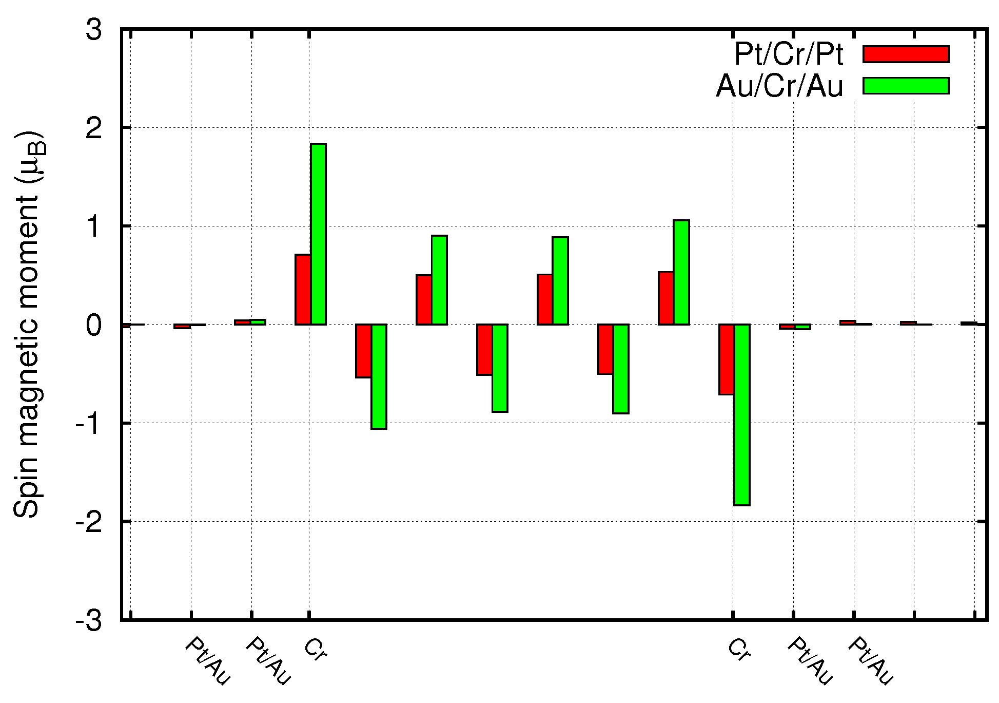
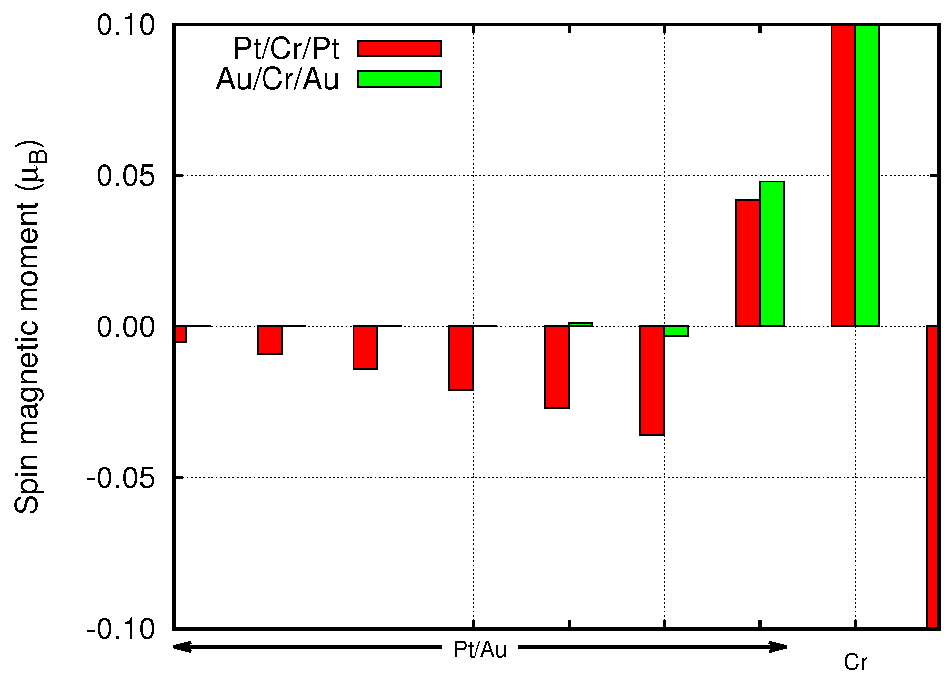
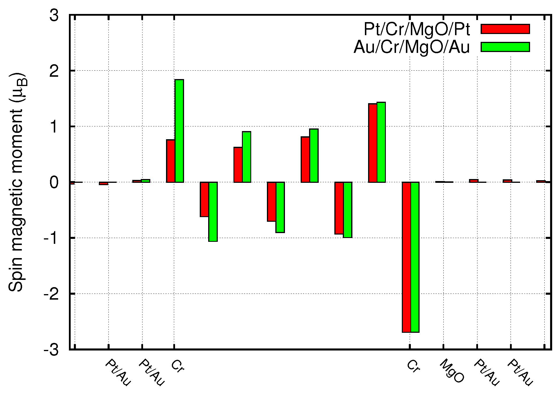
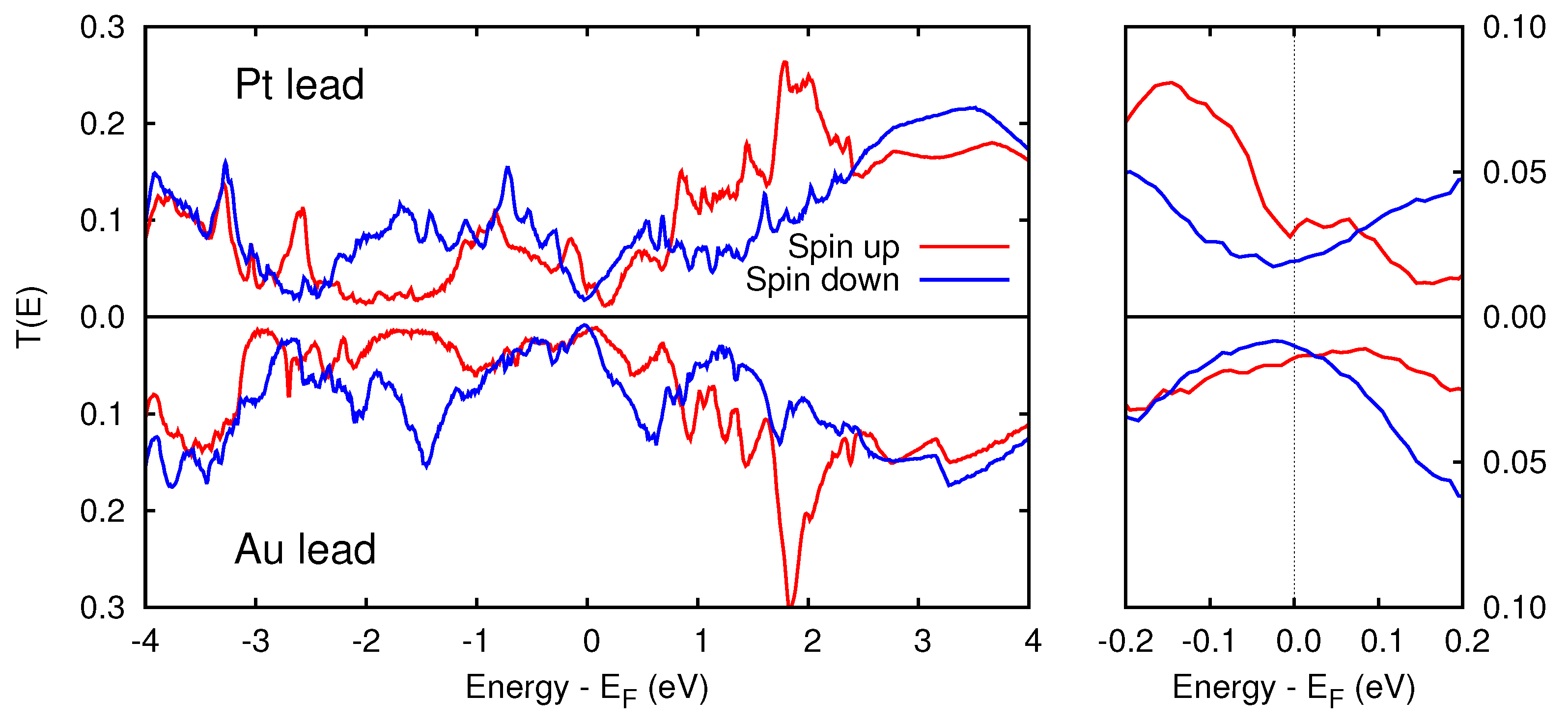
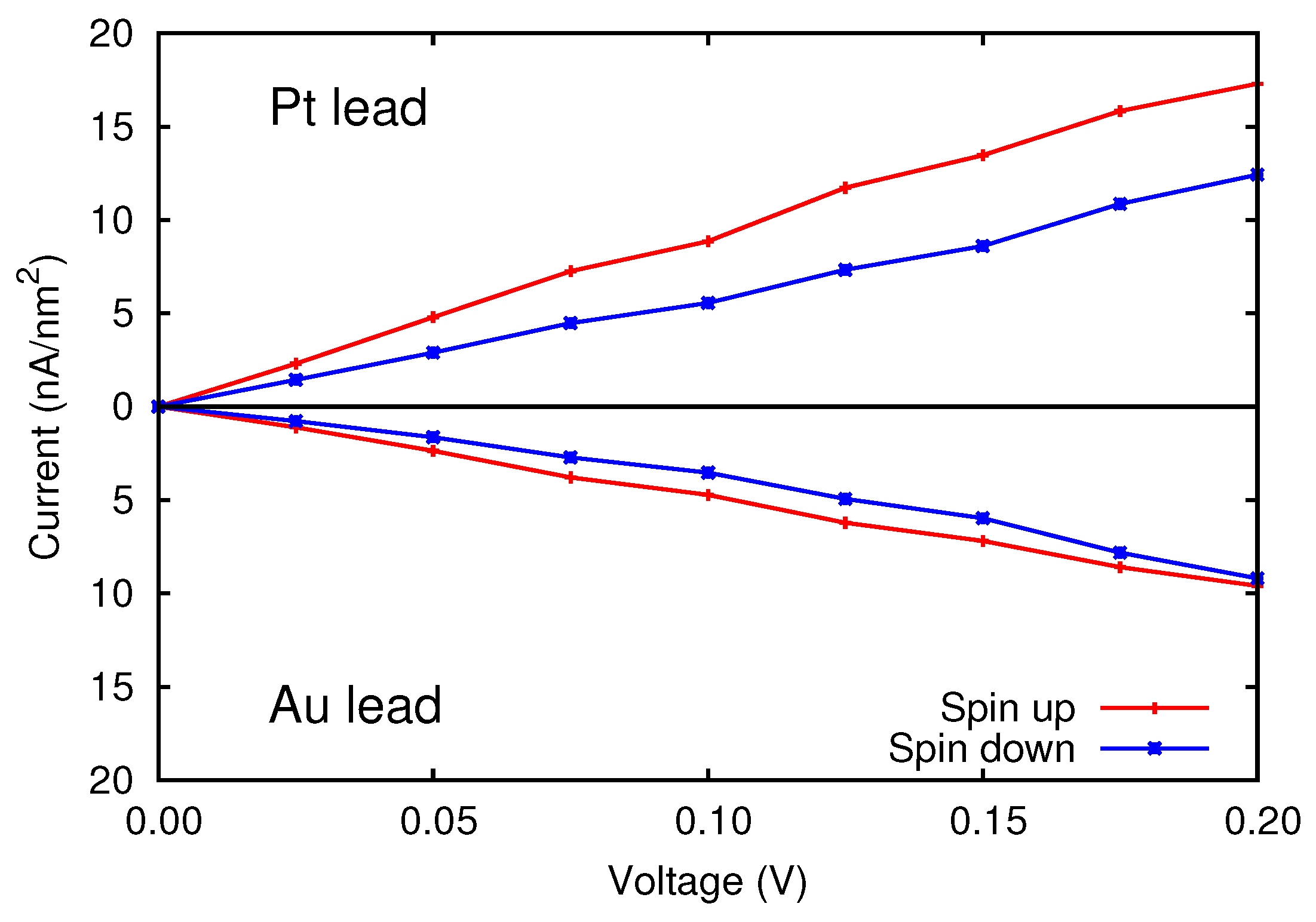
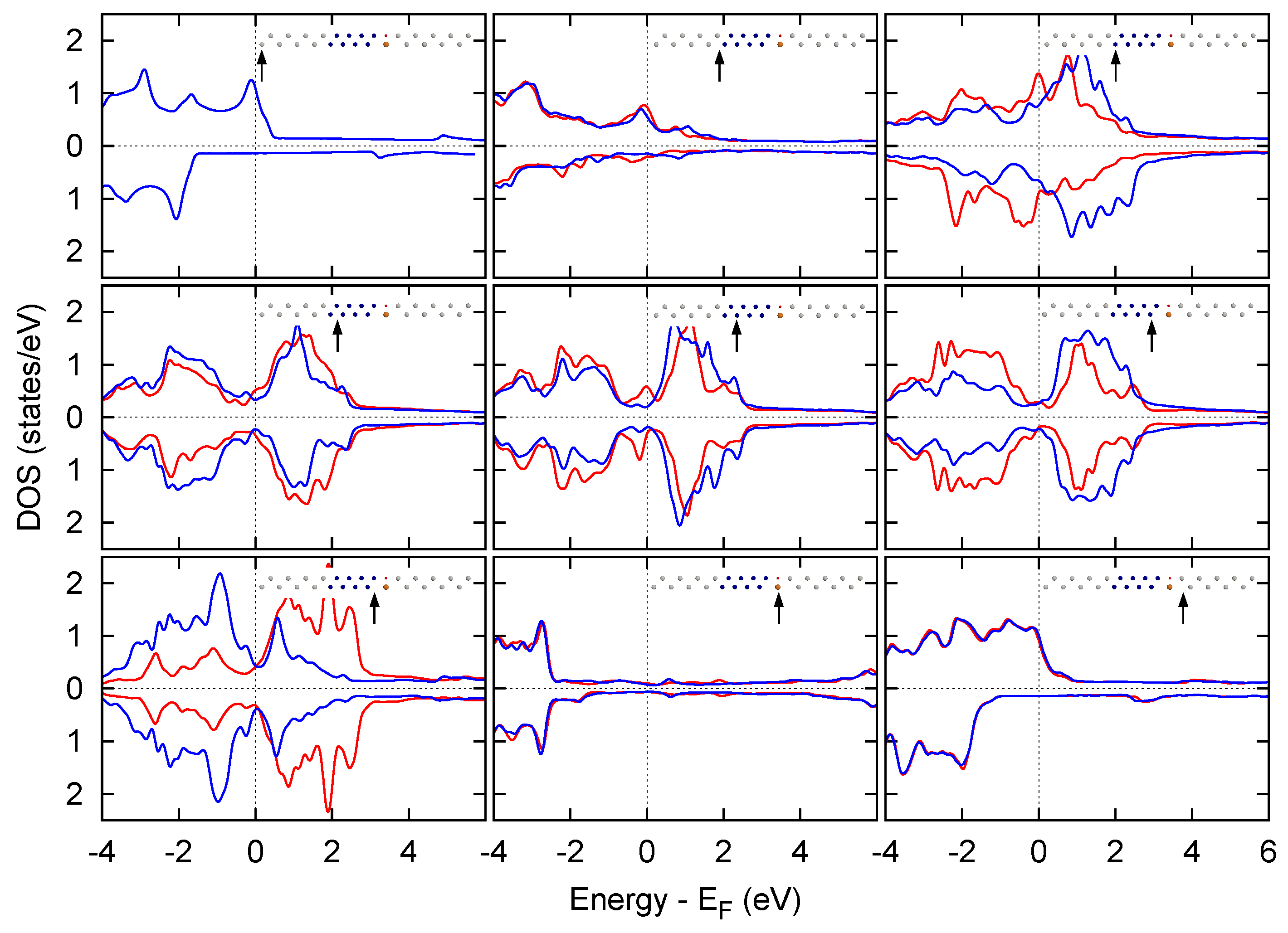
3.2. Metal/Cr/Metal
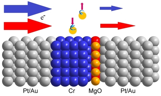
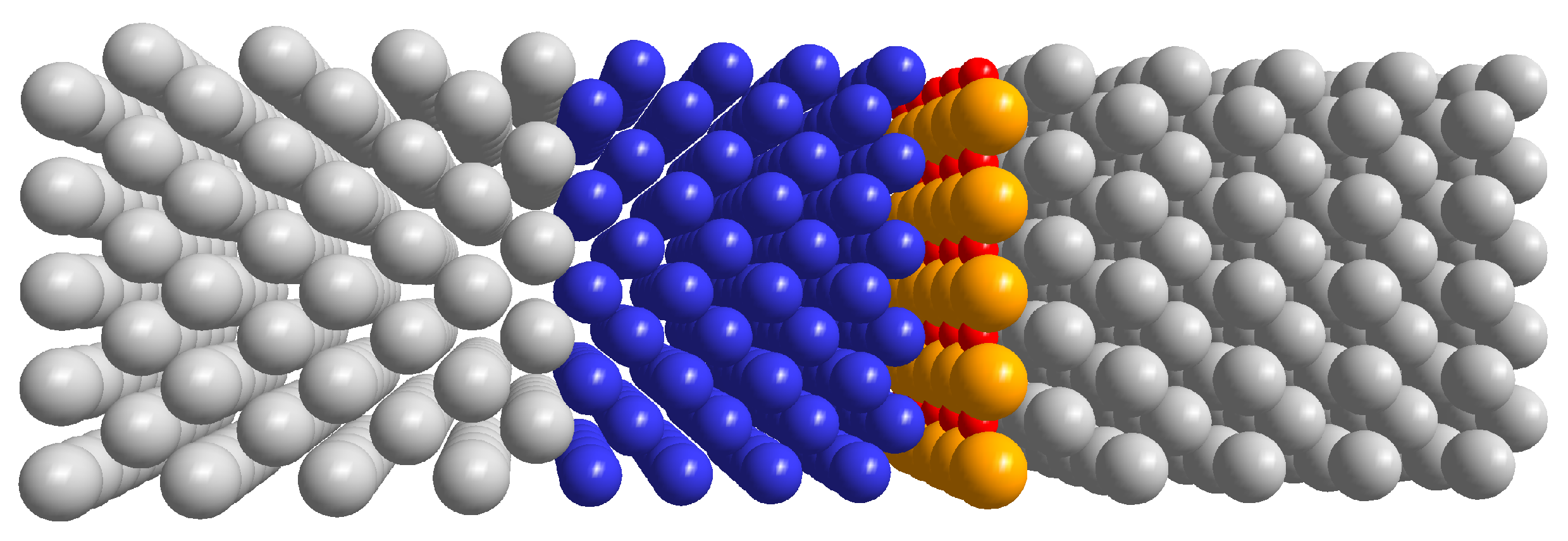
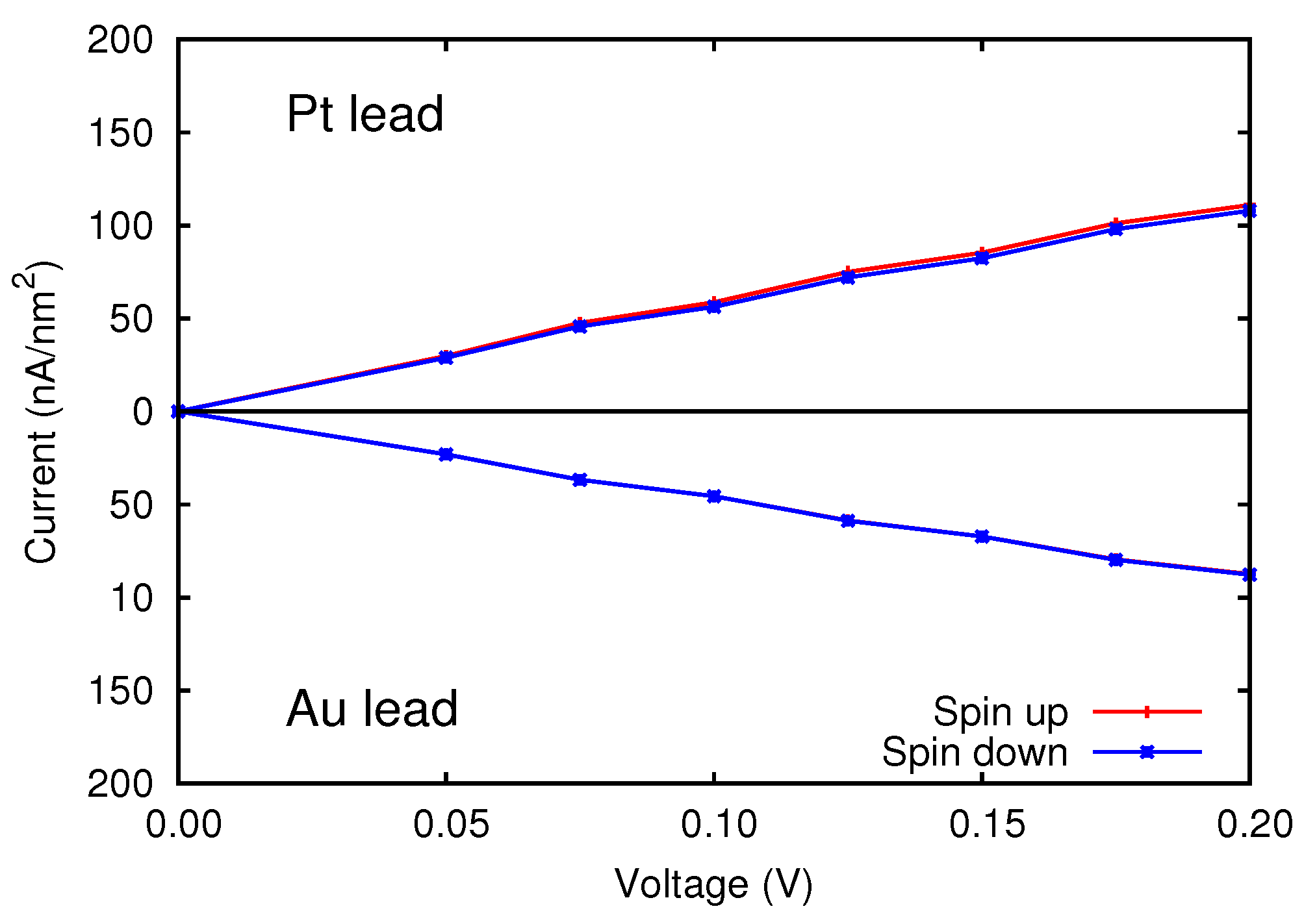
3.3. Metal/Cr/MgO/Metal
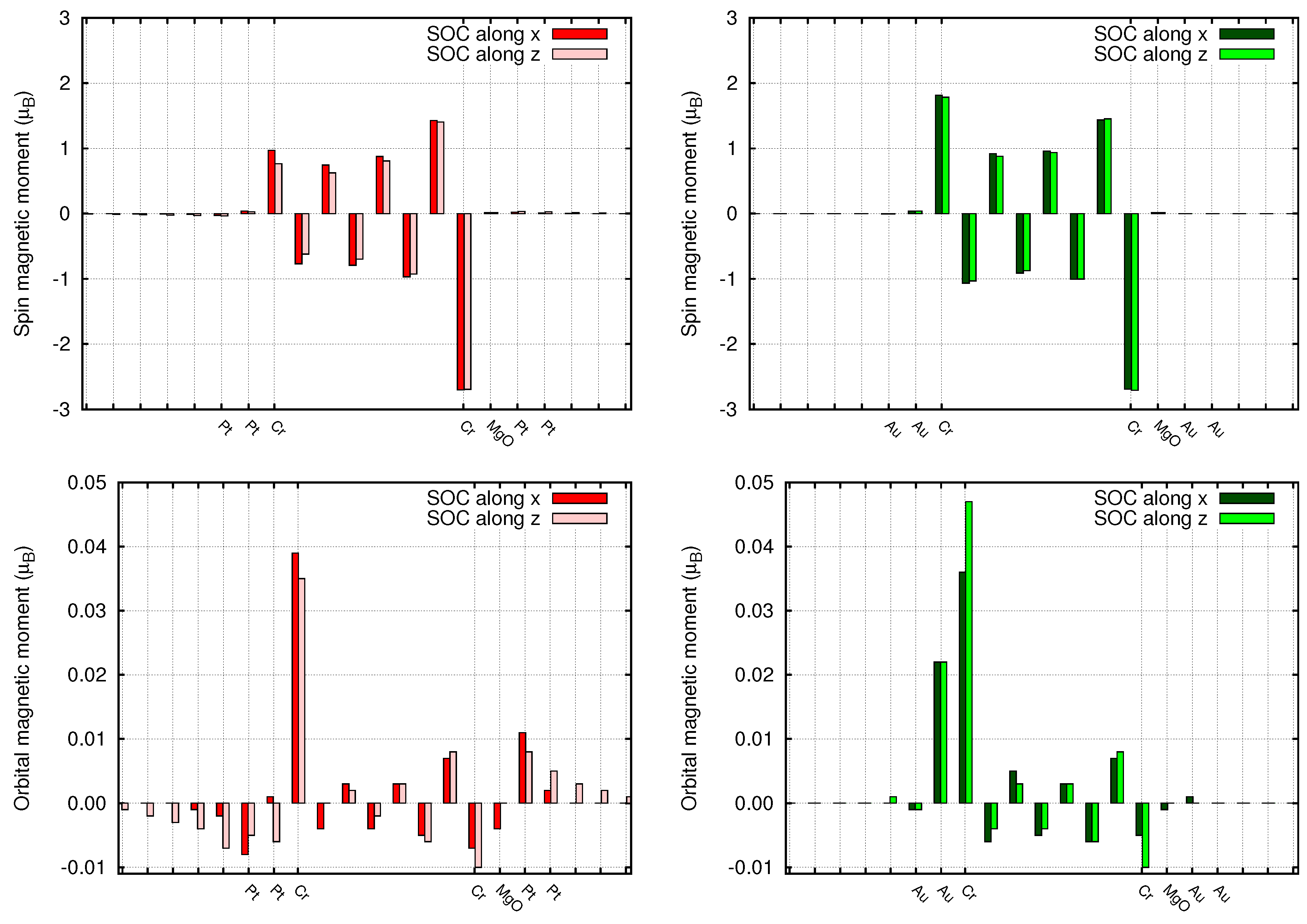
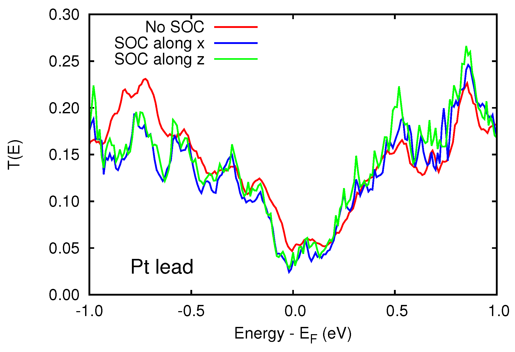
4. Spin-Orbit Calculations
5. Conclusions
Author Contributions
Funding
Acknowledgments
Conflicts of Interest
Abbreviations
| AFM | antiferromagnetic |
| AHE | anomalous Hall effect |
| AMR | anisotropic magnetoresistance |
| COHP | crystal orbitals Hamilton populations |
| DFT | density functional theory |
| DOS | density of states |
| FM | ferromagnetic |
| GGA | generalized gradient approximation |
| GMR | giant magnetoresistance |
| LDA | local density approximation |
| NM | non-magnetic |
| PDOS | projected density of states |
| SOC | spin-orbit coupling |
| TMR | tunnel magnetoresistance |
| XMCD | x-ray magnetic circular dichroism |
References
- Baibich, M.N.; Broto, J.M.; Fert, A.; Nguyen Van Dau, F.; Petroff, F.; Eitenne, P.; Creuzet, G.; Friederich, A.; Chazelas, J. Giant magnetoresistance of (001)Fe/(001)Cr magnetic superlattices. Phys. Rev. Lett. 1988, 61, 2472. [Google Scholar] [CrossRef] [PubMed]
- Binasch, G.; Grünberg, P.; Saurenbach, F.; Zinn, W. Enhanced magnetoresistance in layered magnetic structures with antiferromagnetic interlayer exchange. Phys. Rev. B 1989, 39, 4828. [Google Scholar] [CrossRef]
- Xie, Z.; Lv, H.; Li, L.; Xu, M. The tunneling magnetic resistance in ferromagnetic junctions with spin-filter composite tunnel barriers. J. Magn. Magn. Mater. 2016, 405, 353–357. [Google Scholar] [CrossRef]
- Tang, J.; Ke, Y.; He, W.; Zhang, X.; Zhang, W.; Li, N.; Zhang, Y.; Li, Y.; Cheng, Z. Ultrafast Photoinduced Multimode Antiferromagnetic Spin Dynamics in Exchange-Coupled Fe/RFeO3 (R = Er or Dy) Heterostructures. Adv. Mater. 2018, 30, 1706439. [Google Scholar] [CrossRef] [PubMed]
- Jungwirth, T.; Marti, X.; Wadley, P.; Wunderlich, D. Antiferromagnetic spintronics. Nat. Nanotechnol. 2016, 11, 231–241. [Google Scholar] [CrossRef] [PubMed]
- Belabbes, A.; Bihlmayer, G.; Bechstedt, F.; Blügel, S.; Manchon, A. Hund’s Rule-Driven Dzyaloshinskii- Moriya Interaction at 3d–5d Interfaces. Phys. Rev. Lett. 2016, 117, 247202. [Google Scholar] [CrossRef] [PubMed]
- del Castillo, E.; Achilli, S.; Cargnoni, F.; Ceresoli, D.; Soave, R.; Trioni, M.I. Spin-filtering in graphene junctions with Ti and Co adsorbates. Chem. Phys. 2016, 478, 91–96. [Google Scholar] [CrossRef]
- Hohenberg, P.; Kohn, W. Inhomogeneous electron gas. Phys. Rev. 1964, 136, B864. [Google Scholar] [CrossRef]
- Kohn, W.; Sham, L.J. Self-Consistent Equations Including Exchange and Correlation Effects. Phys. Rev. 1965, 140, A1133. [Google Scholar] [CrossRef]
- Soler, J.M.; Artacho, E.; Gale, J.D.; García, A.; Junquera, J.; Ordejón, P.; Sánchez-Portal, D. The SIESTA method for ab initio order-N materials simulation. J. Phys. Condens. Matter 2002, 14, 2745. [Google Scholar] [CrossRef]
- Ceperley, D.M.; Alder, B.J. Ground state of the electron gas by a stochastic method. Phys. Rev. Lett. 1980, 45, 566. [Google Scholar] [CrossRef]
- Troullier, N.; Martins, J.L. Efficient pseudopotentials for plane-wave calculations. Phys. Rev. B 1991, 43, 1993. [Google Scholar] [CrossRef]
- Cottenier, S.; De Vries, B.; Meersschaut, J.; Rots, M. What density-functional theory can tell us about the spin-density wave in Cr. J. Phys. Condens. Matter 2002, 14, 3275. [Google Scholar] [CrossRef]
- Soulairol, R.; Fu, C.; Barreteau, C. Structure and magnetism of bulk Fe and Cr: From plane waves to LCAO methods. J. Phys. Condens. Matter 2010, 22, 295502. [Google Scholar] [CrossRef] [PubMed]
- Landauer, R. Spatial variation of currents and fields due to localized scatterers in metallic conduction. IBM J. Res. Dev. 1957, 1, 223–231. [Google Scholar] [CrossRef]
- Büttiker, M. Scattering theory of thermal and excess noise in open conductors. Phys. Rev. Lett. 1990, 65, 2901. [Google Scholar] [CrossRef] [PubMed]
- Büttiker, M. Scattering theory of current and intensity noise correlations in conductors and wave guides. Phys. Rev. B 1992, 46, 12485. [Google Scholar] [CrossRef]
- Brandbyge, M.; Mozos, J.L.; Ordejón, P.; Taylor, J.; Stokbro, K. Density-functional method for nonequilibrium electron transport. Phys. Rev. B 2002, 65, 165401. [Google Scholar] [CrossRef]
- Ferrer, J.; Lambert, C.J.; Garcıa-Suarez, V.M.; Manrique, D.Z.; Visontai, D.; Oroszlany, L.; Rodrıguez-Ferradas, R.; Grace, I.; Bailey, S.W.D.; Gillemot, K.; et al. GOLLUM: A next-generation simulation tool for electron, thermal and spin transport. New J. Phys. 2014, 16, 093029. [Google Scholar] [CrossRef]
- Kittel, C. Introduction to Solid State Physics; Wiley: New York, NY, USA, 1996. [Google Scholar]
- Arrott, A.; Werner, S.A. Neutron-Diffraction Study of Dilute Chromium Alloys with Iron. Phys. Rev. 1967, 153, 624. [Google Scholar] [CrossRef]
- Dronskowski, R.; Blochl, P.E. Crystal Orbital Hamilton Populations (COHP): Energy-Resolved Visualization of Chemical Bonding in Solids Based on Density-Functional Calculations. J. Phys. Chem. 1993, 97, 8617. [Google Scholar] [CrossRef]
- Rogalev, A.; Ollefs, K.; Wilhelm, F. X-Ray Magnetic Circular Dichroism. In X-ray Absorption and X-ray Emission Spectroscopy; John Wiley & Sons: Chichester, UK, 2016; Chapter 23; pp. 671–694. [Google Scholar]
- Nagaosa, N.; Sinova, J.; Onoda, S.; MacDonald, A.H.; Ong, N.P. Anomalous Hall effect. Rev. Mod. Phys. 2010, 82, 1539. [Google Scholar] [CrossRef]
- Guo, G.Y.; Murakami, S.; Chen, T.W.; Nagaosa, N. Intrinsic Spin Hall Effect in Platinum: First-Principles Calculations. Phys. Rev. Lett. 2008, 100, 096401. [Google Scholar] [CrossRef] [PubMed]


© 2018 by the authors. Licensee MDPI, Basel, Switzerland. This article is an open access article distributed under the terms and conditions of the Creative Commons Attribution (CC BY) license (http://creativecommons.org/licenses/by/4.0/).
Share and Cite
Bragato, M.; Achilli, S.; Cargnoni, F.; Ceresoli, D.; Martinazzo, R.; Soave, R.; Trioni, M.I. Magnetic Moments and Electron Transport through Chromium-Based Antiferromagnetic Nanojunctions. Materials 2018, 11, 2030. https://doi.org/10.3390/ma11102030
Bragato M, Achilli S, Cargnoni F, Ceresoli D, Martinazzo R, Soave R, Trioni MI. Magnetic Moments and Electron Transport through Chromium-Based Antiferromagnetic Nanojunctions. Materials. 2018; 11(10):2030. https://doi.org/10.3390/ma11102030
Chicago/Turabian StyleBragato, Marco, Simona Achilli, Fausto Cargnoni, Davide Ceresoli, Rocco Martinazzo, Raffaella Soave, and Mario Italo Trioni. 2018. "Magnetic Moments and Electron Transport through Chromium-Based Antiferromagnetic Nanojunctions" Materials 11, no. 10: 2030. https://doi.org/10.3390/ma11102030
APA StyleBragato, M., Achilli, S., Cargnoni, F., Ceresoli, D., Martinazzo, R., Soave, R., & Trioni, M. I. (2018). Magnetic Moments and Electron Transport through Chromium-Based Antiferromagnetic Nanojunctions. Materials, 11(10), 2030. https://doi.org/10.3390/ma11102030