Tunable Coupled-Resonator-Induced Transparency in a Photonic Crystal System Based on a Multilayer-Insulator Graphene Stack

1
College of Electronic Science and Engineering, National University of Defense Technology, Changsha 410073, China
2
School of Physical and Electronic Science, Changsha University of Science and Technology, Changsha 410114, China
*
Author to whom correspondence should be addressed.
Materials 2018, 11(10), 2042; https://doi.org/10.3390/ma11102042
Submission received: 18 September 2018
/
Revised: 16 October 2018
/
Accepted: 17 October 2018
/
Published: 19 October 2018
(This article belongs to the Special Issue Transparent Conductive Films and Their Applications)
Abstract
:We achieve the effective modulation of coupled-resonator-induced transparency (CRIT) in a photonic crystal system which consists of photonic crystal waveguide (PCW), defect cavities, and a multilayer graphene-insulator stack (MGIS). Simulation results show that the wavelength of transparency window can be effectively tuned through varying the chemical potential of graphene in MGIS. The peak value of the CRIT effect is closely related to the structural parameters of our proposed system. Tunable Multipeak CRIT is also realized in the four-resonator-coupled photonic crystal system by modulating the chemical potentials of MGISs in different cavity units. This system paves a novel way toward multichannel-selective filters, optical sensors, and nonlinear devices.
1. Introduction
The electromagnetically induced transparency (EIT) effect, which is a quantum interference phenomenon that forms a sharp transparency window over a broad transmission spectrum, has a wide range of potential applications in the fields of slow optical propagation, the transfer of quantum correlation, and nonlinear optical processes [1,2,3]. EIT-like optical responses can be obtained in classical resonator systems and many optical devices, such as grating and plasmonic resonator antennas, which has opened up a pathway in photonics, offering potential for smaller devices to be used for the manipulation and transmission of light [4,5]. The EIT-like effect discovered in the coupled-resonator photonic systems is also called coupled-resonator-induced transparency (CRIT). In previous studies, it was theoretically predicted and experimentally demonstrated that the CRIT effect can efficiently provide tunable transparency on the optical chip due to the significant reduction in the threshold power for optical bistability [6,7,8,9,10]. However, varying the optical dispersion relations, symmetries, and spatial distribution once the physical parameters of the system are fixed is difficult, which means the tunability of CRIT would be limited after the fabrication of the whole resonant system.
Since its discovery in 2004, graphene, a monolayer of carbon atoms arranged in a two-dimensional (2D) hexagonal lattice, has received considerable attention due to its electrical and thermal properties, as well as unique atomic thickness [11,12]. An undoped graphene monolayer absorbs approximately 2.3% of normal incident light across the visible and infrared range, which is high given its single atom thickness [13,14]. The conductivity of graphene can be tuned under electric/magnetic biasing or chemical doping; thus, a variety of graphene-based structures have been proposed to achieve many tunable optical responses, such as propagation in optical waveguides, perfect absorption in photonic crystal arrays, resonance on metamaterials, and nonlinear phenomena [15,16]. However, graphene is generally thought to not conduct sufficiently well to replace metals in optical devices, since it is too “thin” to sustain intense resonance [17,18]. To overcome this limitation, multiple graphene structures have been proposed to replace the monolayer graphene due to the enlarged amplitude of the graphene-light interaction. For example, Zhu et al. [19] designed a terahertz fishnet metamaterial consisting of a gallium arsenide substrate sandwiched between multi-layer graphene-dielectric composites, which dynamically controlled the left-handed features by applying external bias to shift the Fermi level in graphene. Su et al. [20] proposed an ultra-thin terahertz metamaterial absorber based on graphene/MgF2 multilayer stacking unit cells arrayed on a gold (Au)-film plane and obtained two total absorption peaks for the incident light in the terahertz range.
In the present study, we design a novel coupled-resonator photonic crystal system, which is composed of a photonic crystal waveguide (PCW) side coupled with two kinds of resonant cavities: one embedded with a multilayer graphene-insulator stack (MGIS) directly coupled to the PCW, and a defect cavity coupled to the first one. The light-graphene interaction in our proposed structure can be significantly enhanced due to the combination of multiple-layer graphene stacks and resonance defect cavities. The transmission spectrum of our proposed system exhibits a transparency window over the resonant band due to the interference between the optical pathways in the two cavities, which reveals a classical CRIT effect. The peak frequency of CRIT can be adjusted by varying the chemical potential of graphene. Furthermore, we design a four-resonator-coupled photonic crystal system and obtain a tunable multipeak CRIT effect.
2. Theoretical Modeling
The top view and side view of MGIS are schematically visualized in Figure 1a. Monolayer graphene with a thickness of hg = 0.34 nm is separated by dielectric layers [21]. Here, we chose Al2O3 as the insulating dielectric with a relative permittivity of , which is also a universal material used in supporting the multiple graphene structures [10,22]. Distributing the carriers into multiple stacks effectively enhances the magnitude of resonance compared with doping in single-layer graphene, which can promote the light-graphene interaction [23]. The thickness of the Al2O3 layer should be a deep subwavelength thickness, but thick enough to avoid the interaction between adjacent graphene layers (e.g., interlayer transitions) [24], thus we define . In addition, the radius of MGIS is set as . The MGIS can be homogenized and viewed as an anisotropic uniaxial medium using the effective medium approximation, and its effective out-of-plane and in-plane permittivities are derived by taking the long-wavelength limit of the Bloch theory [25]:
where and are the permittivity parallel and perpendicular to the horizontal plane, respectively; represents the angular frequency; and is the surface conductivity of monolayer graphene, which contains two contributed portions: represents absorption due to intraband electron-photon scattering, and is caused by the interband electron transition process. Their expressions are given by the Kubo formula [26]:
where is the charge of the electron, T is the temperature, is the reduced Planck constant, is the Boltzmann constant, and is the chemical potential of graphene. represents the damping constant, which can be defined as , where is the Fermi velocity and is the electron mobility [19]. From Equations (1) and (2), the value of is closely connected with the chemical potential, which can be modulated by chemical doping methods or applying gate voltage [27,28].
Composed of periodical silicon medium elements, 2D photonic crystal systems have potential for optical communication given their potential ability to control the propagation of light [29,30]. As shown in Figure 1c, our proposed photonic crystal system mainly consisted of a photonic crystal waveguide (PCW), a directly side-coupled cavity (Cavity A), and a defect cavity (Cavity B). The PCW was formed by removing a specific row of silicon elements, which realize guiding and trapping the transverse-magnetic (TM) light in the remaining empty space as light injected and coupled into the photonic crystal system [31]. The bottom illustration in Figure 1c is the side view of our proposed system. Since the system is fabricated by a periodic silicon rods array, both the top and bottom surface are loaded with silicon substrate to support the whole structure and guarantee the normal propagation of the incident wave in PCW. Figure 1d shows the top view of the proposed system. We defined the lattice constant of our proposed system as 400 nm, the width of the excitation port of PCW as , and the radius of the silicon element as 90 nm. The height of the proposed system was set as 251.4 nm. Cavity A, which was fabricated by embedding the MGIS into the resonant cavity to replace the original silicon element of the structure, was located at distance 2d from the center of the PCW. The radius of the MGIS in Cavity A was equal to , as shown in Figure 1a. The defect cavity Cavity B was formed by a 3 × 3 silicon element array with a periodic radius of . Although the tunable CRIT effect in our paper was only studied in theory and simulated on software, the modeling process of MGIS has already been presented experimentally in previous studies [10,11]. The first step of the process, presented in Figure 1b, is coating the monolayer graphene and dielectric layer by turns to obtain an unpatterned MGIS on the substrate; then, the next step is patterning the unpatterned MGIS into the desirable shape, such as a cylinder; the third step is reserving only one MGIS on the substrate and eliminating the others; and the last step is coating silicon on the substrate and patterning the silicon layer to the photonic crystal system. In the whole of the fabricating process, a great challenge is how to keep the MGIS unpatterned and stable in the last step.
As the incident wave passed through the coupled aperture, the energy was coupled into Cavity A through the dielectric aperture and excited the resonant modes at special wavelengths. Here, the temporal coupled-mode theory can be used to analyze the dynamic transmission characteristics of our proposed system. As shown in Figure 1e, denotes the coupling coefficient between PCW and Cavity A, and is the decay rate due to the internal loss in Cavity A, which is mainly caused by the photonic crystal structure itself. denotes the coupling coefficient between Cavity A and Cavity B. Since the light-graphene interaction in MGIS can absorb considerable injected energy in Cavity A, the value of is closely related to the absorption performance of MGIS. , , and represent the input, reflection, and output field amplitude, respectively, and the differential relationships between the parameters above can be expressed as [32]:
where and denote the normalized amplitude of Cavity A and Cavity B, respectively; and represent the resonant frequency of Cavity A and Cavity B, respectively. Given the power conservation and the time reversal symmetry, the relationship among the amplitudes in PCW can be calculated as: and . In the linear system, since the field everywhere oscillates and the input frequency is , we have and . When the input field is launched to the left port (), the transmission coefficient of the whole system is derived as:
Particularly, without Cavity B, the transmission coefficient can be simplified as:
We calculated the transmission response to verify the CRIT effect of our proposed system when the parameters in Equations (5) and (6) were set to , , , , and . Figure 2a shows the transmission spectrum as the incident wave varies from 900 to 1500 nm, both with and without Cavity B. When Cavity A was not side-coupled with Cavity B, the value of was zero, and the spectrum exhibited a dip at the resonance wavelength due to the destructive interference between the incident wave and the escaped power from Cavity A. However, when Cavity A was side-coupled with Cavity B, a narrow transparency window appeared in the center of a broader transmitted dip, which showed an EIT-like phenomenon. This performance is also known as CRIT, similar to EIT in the atomic system, which is derived from the destructive interference between the two optical pathways passing and bypassing Cavity B. For Equation (5), under the condition of , the value of can be simplified as , which means an obvious transparency window. Figure 2b,c reveal the evolution of the transmission spectrum with the values of and , respectively. The results show that the peak value of the transparency window gradually increased as increased from 1 × 10¹² rad·s−1 to 9 × 10¹² rad·s−1, whereas the frequency corresponding to the transparency window processed a nearly linear blue shift as increased from 3.4 × 10¹⁴ rad·s−1 to 3.6 × 10¹⁴ rad·s−1. The CRIT effect can be used to design bandpass plasmonic filters, thus the coupling coefficients and resonant frequencies of the cavities enable control of the filtering features, such as wavelength and bandwidth [33].
3. Simulation Results
The transmission response of the proposed photonic crystal system was investigated numerically using the rigorous finite element method implemented on software COMSOL. Particularly, we define the scattering boundary condition on the top and bottom surfaces, which can effectively eliminate the losses caused by environments such as substrates. For the permittivity parameters of MGIS mentioned in Equations (1) and (2), at room temperature, we assumed that the chemical potential was 0.8 eV, the Fermi velocity was c/300 m/s, and the electron mobility was 10,000 cm2/Vs. We first simulated the transmission spectrum of our system without Cavity B. Figure 3a (red line) shows that there is a sharp resonant band over the wavelength range from 1240.0 nm to 1280.0 nm, and the transmission coefficient nearly reduced to zero at about 1256.2 nm. In Figure 3b (red line), when Cavity A is coupled with Cavity B, a transparency window is formed in the resonant stop band and the transmission coefficient can reach 0.36 at about 1255.1 nm, which denotes a typical CRIT phenomenon. The results are in good agreement with the theoretical modeling in Figure 2a. Since the permittivity of MGIS can be effectively modulated by tuning the chemical potential of graphene by applying gate voltage, we also discussed the transmission spectrum with different values of . In Figure 3a, the wavelength corresponding to the resonance gradually increases from 1256.2 nm to 1261.8 nm as decreases from 0.8 eV to 0.4 eV. In Figure 3b, the wavelength corresponding to the transparency window displays a red shift to 1260.9 nm and the peak value gradually decreases from 0.36 to 0.17.
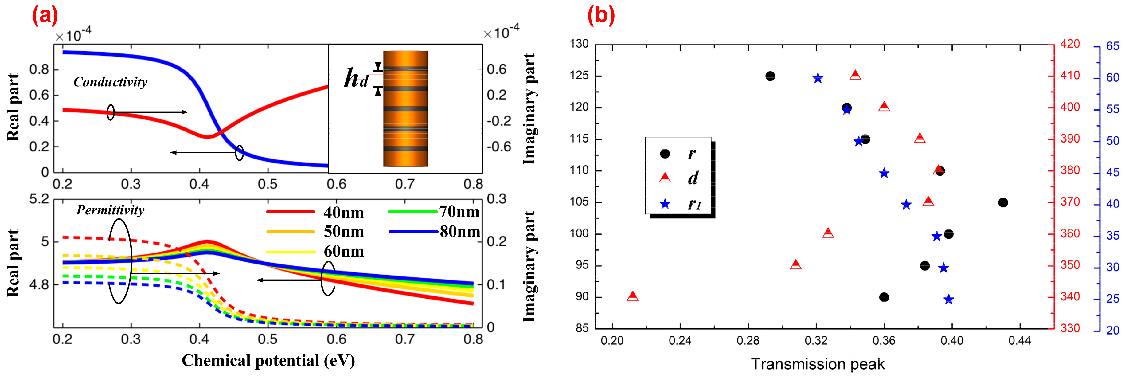
Here, we introduce the dielectric resonator perturbation theory to explain the variation in wavelength corresponding to the resonant band and transparency window along with the chemical potential in Figure 3. According to Equations (1) and (2), we first calculated the value of and at about 1250 nm, corresponding to the photon energy , as shown in Figure 4a. For the conductivity of the monolayer graphene, the real part (blue line) reduced rapidly when was in the region of 0.3 to 0.5 eV, but changed slowly in other regions, while the imaginary part (red line) first decreased and then increased as increased. Thus, we observed that graphene’s conductivity is strongly dispersive and extremely sensitive to the bias Fermi level, which immediately suggests the potential for graphene’s usage in tunable optical metamaterials and metadevices. For the permittivity of MGIS, in contrast to the variation trend of , the real part of (solid line) first increased and then decreased, while the imaginary part (dashed line) reduced rapidly in the region of 0.3 to 0.5 eV, but changed slowly in other regions. Particularly, the modulation amplitude of significantly enhanced as decreased from 80 nm to 40 nm, which means we can improve the tunability of by moderately reducing the thickness of the dielectric layer. Since we only tuned the permittivity of MGIS with relying on the applied voltage and maintained the volume of Cavity A, according to the perturbation theory, the modulation for the resonant frequency of Cavity A under the condition without volume dilatation can be expressed as:
where and represent the E-field intensity and H-field intensity in Cavity A before perturbation, respectively;, , and are the resonant wavelength, permittivity, and permeability of Cavity A before perturbation, respectively; and , , and are the corresponding variations after perturbation. In the case of ,. The permittivity of MGIS displayed a negative relationship with chemical potential in the region of 0.4 to 0.8 eV (Figure 4a), which means the resonant wavelength of Cavity A decreases as increases. The wavelength of the transparency window is positively related to resonant wavelength (Figure 2c). Thus, with analysis combined with the perturbation theory, we drew the conclusion that as increases from 0.4 eV to 0.8 eV, the wavelength of the transparency window shows a blue shift, which perfectly matches the simulation results, as shown in Figure 3b.
From the simulation above, the performance of the CRIT effect was verified to be closely related to the chemical potential of MGIS. The performance can be effectively changed by tuning the structural parameters of the proposed photonic crystal system. Here, we mainly discuss the value of the transparency peak with different parameters, including the radius of the silicon element, the lattice constant , and the radius of the elements in Cavity B. As shown in Figure 4b, defining the chemical potential of graphene at about 0.8 eV, the transparency peak first increased and then declined as r increased from 90 to 125 nm, and reached 0.43 when was equal to 105 nm. A similar trend also occurred as d increased from 340 to 410 nm. These variations can be explained by the appropriate reduction in the lattice constant or increase in the radius of the element alleviating the propagation loss and leading to an improvement of transmission [34,35]. However, a too compact configuration of elements can destroy the periodic property of the whole photonic crystal system and hold the incident wave back to the defect cavity. The decrease in can affect the resonant property of Cavity B, resulting in a gradual increase in the transparency window from 0.32 to 0.4. In order to better understand the physical mechanism of the CRIT effect, we also plotted the power flow distributions when the value of the chemical potential was set as 0.8 eV, which reflected the transmission path of the incident light wave in our proposed system. Figure 5a–c show the power flow distributions corresponding to the dots “a”, “b”, and “c” in Figure 3a, respectively. Consistent with the variation trend in the transmission spectrum, the incident waves can pass through the PCW smoothly at about 1247.1 nm and 1265.3 nm; conversely, the propagation dissipates rapidly and most of the power is concentrated into Cavity A at about 1256.2 nm. These results verify that the resonance band is due to the absorption of MGIS caused by the enhanced graphene-light interaction. Figure 5d–f show the power flow distributions corresponding to the dots “d”, “e”, and “f” in Figure 3b, respectively. There is coherence enhancement between the electric fields in Cavity A and in Cavity B at about 1255.1 nm, whereas the incident light in PCW is in-phase with the wave in Cavity A. Thus, the CRIT effect can also be explained by the interference between the two optical pathways: the direct excitation of resonant mode in Cavity A by the incident wave and the excitation by coupling with Cavity B [36]. The variation in the chemical potential of graphene in MGIS directly affects the interference between the PCW and resonant cavities to change the CRIT effect. In addition, at about 1252.3 nm and 1258.2 nm, there is an anti-phase of the wave between Cavity A and Cavity B, which means the conditions of resonance destruction are perfectly satisfied and lead to the cut-off of propagation.
4. Discussion
4.1. Multipeak CRIT Effect
For the multi-resonator-coupled photonic crystal system in Figure 6a, the dynamic transmission features can be investigated using temporal coupled-mode theory. The transmission coefficient of incident light passing through the ith side-coupled-cavity unit is:
where , , and represent the decay rates in the ith cavity unit; and and are the resonant frequency of cavities. The propagation waves in the PCW should satisfy the relationship in the steady state:
where represents the phase difference between the ith and i + 1th cavity unit, which can be expressed as [37,38]:
where is the separation distance between the ith and i + 1th cavity units, is the light velocity in a vacuum, is the effective refractive index of the fundamental mode in the PCW, and and are the permittivity of vacuum and the MGIS in Cavity A, respectively. is the additional phase shift of Cavity B. Assume that the parameters of the whole system are equal to the values defined in Figure 3. The real part of the refractive index as a function of incident wavelength calculated by Equation (11) is shown in Figure 6b. When , the value of gradually decreases from 1.472 to 1.401 as the wave frequency increases from 1000 nm to 1400 nm. Since the permittivity of graphene is modulated with the chemical potential, we found that the integral level of the refractive index declined as reduced to 0.4 eV. In addition, Figure 6b shows the value of as a function of incident wavelength (black dotted line) when , which makes the value of satisfy the odd times of π. In the region of , the variation in tends to be stable. As a result, according to Equations (10) and (11), to realize a multipeak CRIT effect in our proposed system, both the distance between adjacent cavity units and the resonant property of each cavity are important factors.
A four-resonator-coupled photonic crystal system was designed as an example to investigate the multipeak CRIT effect. The separations of adjacent cavity units (, , and ) were set to 2800 nm uniformly, which is precisely seven times the lattice constant . The wavelength of the transparency window in Figure 3 could be tuned from 1255.1 nm to 1260.9 nm by tuning the chemical potential of graphene from 0.8 eV to 0.4 eV. However, this modulation was far from the satisfactory range to achieve the multi-wavelength CRIT effect. An effective method to broaden the modulated range of resonance is changing the radius of the unit in the defect cavity (the unit here is MGIS), which was a common method used to realize the multi-mode effect in prior studies [39,40]. As a result, the radius of MGIS in our proposed structure was set to 45, 47, 49, and 51 nm,. Assume that the chemical potentials of graphene in different cavity units are defined as , , , and . Figure 7a reveals the transmission spectrum over the wavelength range from 1240 nm to 1290 nm on the condition that . In this case, there are four transparency peaks (peak 1 to peak 4) located at 1256.4, 1262.1, 1269.9, and 1277.5 nm, respectively, with peak values of about 0.38, 0.31, 0.19, and 0.23, respectively. The difference in peak values can be explained by two reasons: the difference in the coupling effect between Cavity A and Cavity B at different wavelengths and the interference between adjacent cavity units. To further investigate the tunability of our proposed system with MGIS, we tuned the value of to 0.68 eV and the value of to 0.89 eV and found that peak 1 and peak 2 combined into one peak at about 1257.1 nm with a peak value of 0.42, as seen in Figure 7b. This can be explained by the shift in the transparency window along with the chemical potential according to the perturbation theory in Equation (7). Figure 7c illustrates the amalgamation of peaks 3 and 4 at about 1275.2 nm when the values of and were tuned to 0.55 and 0.93 eV, respectively. When further tuning the chemical potential of the MGIS in these four cavity units simultaneously, as shown in Figure 7d, the four transparency peaks in Figure 7a simplified into only two peaks with smaller Q-factors. The modulation property of the multipeak CRIT effect in a multiple cavities system based on MGIS has meaningful applications in terms of broadening the sidelobes of filters and tunable multichannel photonic crystal waveguide.
4.2. Electrical Modulation of MGIS
The voltage required to effectively tune the chemical potential of graphene is the key to achieving tunability of the proposed CRIT effect. Here, the relationship between the chemical potential of graphene and applied voltage can be denoted by [41]:
where (1 × 10⁶ m/s) is the Fermi velocity for graphene and (~24 mF/m2) is the effective capacitance per unit area. The intrinsic carrier concentration is a constant for monolayer graphene, which is about 1.17 × 10¹⁷ m−3. As graphene is supported on the top of an Al2O3 dielectric, can be expressed as [42]:
where (~8.854 × 10⁻¹² F/m) denotes the permittivity of the vacuum and denotes the offset voltage caused by doping, which can be obtained from Equations (12) and (13) as varies with the thickness of Al2O3, as well as the offset voltage . As shown in Figure 8, assuming that is equal to zero, the required to tune increasing from 0.4 eV to 0.8 eV decreases from 52.9 V to 24.4 V as decreases from 80 nm to 40 nm. By fixing the value of at 50 nm and improving from 1 to 5 V, we found that can further decrease to 5.9 V, which means that using doped graphene in MGIS is an effective method to create a realistic tunable CRIT effect in our proposed system suitable for practical application.
5. Conclusions
In this study, we proposed a novel photonic crystal system, which includes a PCW and a defect cavity side-coupled with a resonant cavity embedded with MGIS. As confirmed by simulations on COMSOL, the resonant wavelength of CRIT in our designed system could be effectively tuned from 1255.1 nm to 1260.9 nm as the chemical potential of MGIS decreased from 0.8 eV to 0.4 eV. Meanwhile, the value of the transmission peak is verified to be closely related to the structural parameters, such as the lattice constant, radius of silicon unit in defect cavity, and so on. In addition, a multipeak CRIT effect was realized in a four-resonator-coupled photonic crystal system. By tuning the chemical potentials of MGISs in different cavities felicitously, we can obtain four-peak CRIT, three-peak CRIT, and two-peak CRIT. What is more, we also found that the voltage required to tune the chemical potential of MGIS from 0.8 eV to 0.4 eV can be effectively reduced to 5.9 V via doping graphene. All these results confirm the excellent characteristics of our proposed system, which provides promise for further research in the field of graphene-based integrated nanophotonic devices, multichannel-selective filters, and optical sensors.
Author Contributions
Conceptualization, J.T. and H.L.; Methodology, H.L.; Software, H.L. and P.L.; Validation, H.L., P.L. and L.B.; Formal Analysis, S.Z.; Investigation, L.B.; Resources, P.L.; Data Curation, H.L.; Writing-Original Draft Preparation, H.L.; Writing-Review & Editing, H.L.; Visualization, H.L.; Supervision, P.L.; Project Administration, S.Z.; Funding Acquisition, P.L.
Funding
This research was funded by the Nature Science Foundation of China (Grants: No. 61372029 and No. 61601491).
Conflicts of Interest
The authors declare no conflict of interest.
References
- Cao, G.T.; Li, H.J.; Zhan, S.P.; Xu, H.Q.; Liu, Z.M.; He, Z.H.; Wang, Y. Formation and evolution mechanisms of plasmon-induced transparency in MDM waveguide with two stub resonators. Opt. Express 2013, 21, 9198–9205. [Google Scholar] [CrossRef] [PubMed]
- Lu, H.; Liu, X.M.; Mao, D. Plasmonic analog of electromagnetically induced transparency in multi-nanoresonator-coupled waveguide systems. Phys. Rev. A 2012, 85, 053803. [Google Scholar] [CrossRef]
- Fleischhauer, M.; Imamoglu, A.; Marangos, J.P. Electromagnetically induced transparency: Optics in coherent media. Rev. Mod. Phys. 2005, 77, 633. [Google Scholar] [CrossRef]
- Lai, G.; Liang, R.S.; Zhang, Y.J.; Bian, Z.Y.; Yi, L.X.; Zhan, G.Z.; Zhao, R.T. Double plasmonic nanodisks design for electromagnetically induced transparency and slow light. Opt. Express 2015, 23, 6554–6561. [Google Scholar] [CrossRef] [PubMed]
- Yang, X.; Yu, M.; Kwong, D.L.; Wong, C.W. All-optical analog to electromagnetically induced transparency in multiple coupled photonic crystal cavities. Phys. Rev. Lett. 2009, 102, 173902. [Google Scholar] [CrossRef] [PubMed]
- Huo, Y.J.; Sandhu, S.; Pan, J.; Stuhrmann, N.; Povinelli, M.L.; Kahn, J.M.; Harris, J.S.; Fejer, M.M.; Fan, S.H. Experimental demonstration of two methods for controlling the group delay in a system with photonic-crystal resonators coupled to a waveguide. Opt. Lett. 2011, 36, 1482–1484. [Google Scholar] [CrossRef] [PubMed]
- Mingaleev, S.F.; Miroshnichenko, A.E.; Kivshar, Y.S. Low-threshold bistability of slow light in photonic-crystal waveguides. Opt. Express 2007, 15, 12380–12385. [Google Scholar] [CrossRef] [PubMed]
- Vlasov, Y.A.; McNab, S.J. Coupling into the slow light mode in slab-type photonic crystal waveguides. Opt. Lett. 2006, 31, 50–52. [Google Scholar] [CrossRef] [PubMed] [Green Version]
- Lu, H.; Liu, X.; Wang, L.; Gong, Y.; Mao, D. Ultrafast all-optical switching in nanoplasmonic waveguide with Kerr nonlinear resonator. Opt. Express 2011, 19, 2910–2915. [Google Scholar] [CrossRef] [PubMed]
- Yan, H.G.; Li, X.S.; Chandra, B.; Tulevski, G.; Wu, Y.Q.; Freitag, M.; Zhu, W.J.; Avouris, P.; Xia, F.N. Tunable infrared plasmonic devices using graphene/insulator stacks. Nat. Nanotechnol. 2012, 7, 330. [Google Scholar] [CrossRef] [PubMed]
- Chang, Y.C.; Liu, C.H.; Liu, C.H.; Zhang, S.; Marder, S.R.; Narimanov, E.E.; Zhong, Z.; Norris, T.B. Realization of mid-infrared graphene hyperbolic metamaterials. Nat. Commun. 2016, 7, 10568. [Google Scholar] [CrossRef] [PubMed] [Green Version]
- Pasanen, P.; Voutilainen, M.; Helle, M.; Song, X.; Hakonen, P.J. Graphene for future electronics. Phys. Scr. 2012, 2012, 014025. [Google Scholar] [CrossRef]
- Hao, R.; Du, W.; Chen, H.S.; Jin, X.F.; Yang, L.Z.; Li, E.P. Ultra-compact optical modulator by graphene induced electro-refraction effect. Appl. Phys. Lett. 2013, 103, 061116. [Google Scholar] [CrossRef]
- Huang, X.J.; Leng, T.; Georgiou, T.; Abraham, J.; Nair, R.R.; Novoselov, K.S.; Hu, Z.R. Graphene oxide dielectric permittivity at GHz and it applications for wireless humidity sensing. Sci. Rep. 2018, 8, 43. [Google Scholar] [CrossRef] [PubMed]
- Madani, A.; Babaei, M. Tunable polarization sensitive absorber made of graphene-based hyperbolic metamaterials. Superlattice Microst. 2017, 102, 470–476. [Google Scholar] [CrossRef]
- Bian, L.A.; Liu, P.G.; Han, Z.Z.; Li, G.S.; Mao, J. Near-unity absorption in a graphene-embedded defective photonic crystals array. Superlattice Microst. 2017, 104, 461–469. [Google Scholar] [CrossRef]
- Tassin, P.; Koschny, T.; Kafesaki, M.; Soukoulis, C.M. A comparison of graphene, superconductors and metals as conductors for metamaterials and plasmonics. Nat. Photonics 2012, 6, 259–264. [Google Scholar] [CrossRef] [Green Version]
- Liu, H.Q.; Liu, P.G.; Bian, L.A.; Liu, C.X.; Zhou, Q.H. An electro-optic modulator side-coupled with photonic crystal nanobeam loaded graphene/Al2O3 multilayer stack. Opt. Mat. Express 2018, 8, 761–774. [Google Scholar] [CrossRef]
- Zhu, W.R.; Xiao, F.J.; Kang, M.; Sikdar, D.; Premaratne, M.L. Tunable terahertz left-handed metamaterial based on multi-layer graphene-dielectric composite. Appl. Phys. Lett. 2014, 104, 051902. [Google Scholar] [CrossRef]
- Su, Z.X.; Yin, J.B.; Zhao, X.P. Terahertz dual-band metamaterial absorber based on graphene/MgF2 multilayer structures. Opt. Express 2015, 23, 1679–1690. [Google Scholar] [CrossRef] [PubMed]
- Vicarelli, L.; Vitiello, M.S.; Coquillat, D.; Lombardo, A.; Ferrari, A.C.; Knap, W.; Polini, M.; Pellegrini, V.; Tredicucci, A. Graphene field-effect transistors as room-temperature terahertz detectors. Nat. Mater. 2012, 11, 865–871. [Google Scholar] [CrossRef] [PubMed] [Green Version]
- Dong, Y.F.; Liu, P.G.; Yu, D.W.; Li, G.S.; Tao, F. Dual-band reconfigurable terahertz patch antenna with graphene-stack-based backing cavity. IEEE Antenna Wirel. Propag. Lett. 2016, 1536, 1541–1544. [Google Scholar] [CrossRef]
- Othman, M.A.K.; Guclu, C.; Capolino, F. Graphene-based tunable hyperbolic metamaterials and enhanced near-field absorption. Opt. Express 2013, 21, 7614–7632. [Google Scholar] [CrossRef] [PubMed]
- Balandin, A.A.; Ghosh, S.; Bao, W.; Calizo, I.; Teweldebrhan, D.; Miao, F.; Lau, C.N. Superior thermal conductivity of single-layer graphene. Nano Lett. 2008, 8, 902–907. [Google Scholar] [CrossRef] [PubMed]
- Wangberg, R.; Elser, J.; Narimanov, E.E.; Podolskiy, V.A. Nonmagnetic nanocomposites for optical and infrared negative-refractive-index media. J. Opt. Soc. Am. B 2006, 23, 498–505. [Google Scholar] [CrossRef]
- Novoselov, K.S.; Fal, V.I.; Colombo, L.; Gellert, P.R.; Schwab, M.G.; Kim, K. A roadmap for graphene. Nature 2012, 490, 192–200. [Google Scholar] [CrossRef] [PubMed]
- Chen, S.S.; Wu, Q.Z.; Mishra, C.; Kang, J.Y.; Zhang, H.J.; Cho, K.; Cai, W.W.; Balandin, A.A.; Ruoff, R.S. Thermal conductivity if isotopically modified graphene. Nat. Mater. 2012, 11, 203–207. [Google Scholar] [CrossRef] [PubMed]
- Farhat, M.; Rockstuhl, C.; Bagci, H. A 3D tunable and multi-frequency graphene plasmonic cloak. Opt. Express 2013, 21, 12592–12603. [Google Scholar] [CrossRef] [PubMed] [Green Version]
- Zhao, Y.; Qian, C.; Qiu, K.; Gao, Y.; Xu, X. Ultrafast optical switching using photonic molecules in photonic crystal waveguides. Opt. Express 2015, 23, 9211–9220. [Google Scholar] [CrossRef] [PubMed]
- Li, J.T.; White, T.P.; Faolain, L.O.; Iglesias, A.G.; Krauss, T.F. Systematic design of flat band slow light in photonic crystal waveguides. Opt. Express 2008, 16, 6227–6232. [Google Scholar] [CrossRef] [PubMed]
- Zhou, H.; Gu, T.Y.; McMillan, J.F.; Yu, M.B.; Lo, G.Q.; Kwong, D.L.; Feng, G.Y.; Zhou, S.H.; Wong, C.W. Enhanced photoresponsivity in graphene-silicon slow-light photonic crystal waveguides. Appl. Phys. Lett. 2016, 108, 111106. [Google Scholar] [CrossRef] [Green Version]
- Tang, B.; Dai, L.; Jiang, C. Electromagnetic response of a compound plasmonic–dielectric system with coupled-grating-induced transparency. Phys. Lett. A 2012, 376, 1234–1238. [Google Scholar] [CrossRef]
- Lu, H.; Liu, X.M.; Wang, G.X.; Mao, D. Tunable high-channel-count bandpass plasmonic filters based on an analogue of electromagnetically induced transparency. Nanotechnology 2012, 23, 444003. [Google Scholar] [CrossRef] [PubMed]
- Hughes, S.; Ramunno, L.; Young, J.F.; Sipe, J.E. Extrinsic optical scattering loss in photonic crystal waveguides: Role of fabrication disorder and photon group velocity. Phys. Rev. Lett. 2005, 94, 033903. [Google Scholar] [CrossRef] [PubMed]
- McNab, S.J.; Moll, N.; Vlasov, Y.A. Ultra-low loss photonic intergrated circuit with membrane-type photonic crystal waveguides. Opt. Express 2003, 11, 2927–2939. [Google Scholar] [CrossRef] [PubMed]
- Chen, Z.; Wang, W.H.; Cui, L.; Yu, L.; Duan, G.Y.; Zhao, Y.F.; Xiao, J.H. Spectral splitting based on electromagnetically induced transparency in plasmonic waveguide resonator system. Plasmonics 2015, 10, 721–727. [Google Scholar] [CrossRef]
- Han, Z.; Forsberg, E.; He, S. Surface plasmon Bragg gratings formed in metal-insulator-metal waveguides. IEEE Photon. Technol. Lett. 2007, 19, 91–93. [Google Scholar] [CrossRef]
- Gong, Y.; Liu, X.; Wang, L. High-channel-count plasmonic filter with the metal-insulator-metal Fibonacci-sequence gratings. Opt. Lett. 2010, 35, 285–287. [Google Scholar] [CrossRef] [PubMed]
- Fussell, D.P.; Hughes, S.; Dignam, M.M. Influence of fabrication disorder on the optical properties of coupled-cavity photonic crystal waveguides. Phys. Rev. B 2008, 78, 144201. [Google Scholar] [CrossRef]
- Varmazyari, V.; Habibiyan, H.; Ghafoorifard, H. All-optical tunable slow light achievement in photonic crystal coupled-cavity waveguides. Appl. Opt. 2013, 52, 6497–6505. [Google Scholar] [CrossRef] [PubMed]
- Pan, T.; Qiu, C.; Wu, J.; Jiang, X.; Liu, B.; Yang, Y.; Zhou, H.; Soref, R.; Su, Y. Analysis of an electro-optic modulator based on a graphene-silicon hybrid 1D photonic crystal nanobeam cavity. Opt. Express 2015, 23, 23357–23364. [Google Scholar] [CrossRef] [PubMed]
- Majumdar, A.; Kim, J.; Vuckovic, J.; Wang, F. Electrical Control of Photonic Crystal Cavity by Graphene. In Proceedings of the CLEO: Science and Innovations 2013, San Jose, CA, USA, 9–14 June 2013. [Google Scholar]
Figure 1.
(a) The top view and side view of a multilayer graphene-insulator stack (MGIS) and (b) the modeling process of MGIS. (c) Schematic perspective view (the bottom illustration shows the side view), (d) top view, and (e) propagating model of the proposed photonic crystal system.
Figure 1.
(a) The top view and side view of a multilayer graphene-insulator stack (MGIS) and (b) the modeling process of MGIS. (c) Schematic perspective view (the bottom illustration shows the side view), (d) top view, and (e) propagating model of the proposed photonic crystal system.

Figure 2.
(a) Transmission spectrum of the proposed system calculated by the temporal coupled-mode theory. (b) Evolution of transmission spectrum with the coupling coefficient varying from 1 × 10¹² rad·s−1 to 9 × 10¹² rad·s−1 when the other parameters are fixed. (c) Evolution of transmission spectrum with the resonant frequency of Cavity A varying from 3.4 × 10¹⁴ rad·s−1 to 3.6 × 10¹⁴ rad·s−1 when the other parameters are fixed.

Figure 3.
Simulation results of transmission spectrum of our proposed photonic crystal system as the chemical potential of MGIS varies from 0.8 eV to 0.4 eV, in (a) without Cavity B and (b) with Cavity B.
Figure 3.
Simulation results of transmission spectrum of our proposed photonic crystal system as the chemical potential of MGIS varies from 0.8 eV to 0.4 eV, in (a) without Cavity B and (b) with Cavity B.

Figure 4.
(a) At a wavelength of 1250 nm, the conductivity of the monolayer graphene (blue line represents real part and red line represents imaginary part) and the in-plane permittivity of MGIS with different values of (solid line represents real part and dotted line represents imaginary part) as a function of . (b) The variation trend in the transmission peak when with different structural parameters.

Figure 5.
In case of , the power flow distribution of our proposed photonic crystal system without Cavity B at about (a) 1247.1 nm, (b) 1256.2 nm, and (c) 1265.3 nm, and with Cavity B at about (d) 1252.3 nm, (e) 1255.1 nm, and (f) 1258.2 nm.
Figure 5.
In case of , the power flow distribution of our proposed photonic crystal system without Cavity B at about (a) 1247.1 nm, (b) 1256.2 nm, and (c) 1265.3 nm, and with Cavity B at about (d) 1252.3 nm, (e) 1255.1 nm, and (f) 1258.2 nm.

Figure 6.
(a) Propagation model of the multi-nanoresonator-coupled photonic crystal systems. (b) Real part of the effective refractive index in the PCW with and the approximately optimal separation corresponds to the adjacent cavity units phase equal to for the central wavelength.
Figure 6.
(a) Propagation model of the multi-nanoresonator-coupled photonic crystal systems. (b) Real part of the effective refractive index in the PCW with and the approximately optimal separation corresponds to the adjacent cavity units phase equal to for the central wavelength.

Figure 7.
Transmission spectrum of our proposed four-resonator-coupled photonic crystal system when: (a) ; (b) , , and ; (c) , , and ; and (d) , , , and .
Figure 7.
Transmission spectrum of our proposed four-resonator-coupled photonic crystal system when: (a) ; (b) , , and ; (c) , , and ; and (d) , , , and .

Figure 8.
The relationship between and for different thicknesses of the Al2O3 layer considering the offset voltage caused by doping on graphene.
Figure 8.
The relationship between and for different thicknesses of the Al2O3 layer considering the offset voltage caused by doping on graphene.

© 2018 by the authors. Licensee MDPI, Basel, Switzerland. This article is an open access article distributed under the terms and conditions of the Creative Commons Attribution (CC BY) license (http://creativecommons.org/licenses/by/4.0/).
Share and Cite
MDPI and ACS Style
Liu, H.; Tan, J.; Liu, P.; Bian, L.-a.; Zha, S. Tunable Coupled-Resonator-Induced Transparency in a Photonic Crystal System Based on a Multilayer-Insulator Graphene Stack. Materials 2018, 11, 2042. https://doi.org/10.3390/ma11102042
AMA Style
Liu H, Tan J, Liu P, Bian L-a, Zha S. Tunable Coupled-Resonator-Induced Transparency in a Photonic Crystal System Based on a Multilayer-Insulator Graphene Stack. Materials. 2018; 11(10):2042. https://doi.org/10.3390/ma11102042
Chicago/Turabian StyleLiu, Hanqing, Jianfeng Tan, Peiguo Liu, Li-an Bian, and Song Zha. 2018. "Tunable Coupled-Resonator-Induced Transparency in a Photonic Crystal System Based on a Multilayer-Insulator Graphene Stack" Materials 11, no. 10: 2042. https://doi.org/10.3390/ma11102042
Note that from the first issue of 2016, this journal uses article numbers instead of page numbers. See further details here.