Investigation of the Electrical Characteristics of Bilayer ZnO/In2O3 Thin-Film Transistors Fabricated by Solution Processing

1
Department of Electronic Engineering, Hallym University, Chuncheon 24252, Korea
2
Department of Environmental Sciences & Biotechnology, Hallym University, Chuncheon 24252, Korea
3
School of Software, Hallym University, Chuncheon 24252, Korea
*
Author to whom correspondence should be addressed.
†
These authors contributed equally to this work.
Materials 2018, 11(11), 2103; https://doi.org/10.3390/ma11112103
Submission received: 2 October 2018
/
Revised: 23 October 2018
/
Accepted: 25 October 2018
/
Published: 26 October 2018
(This article belongs to the Special Issue Selected Papers from IEEE ICASI 2018)
Abstract
:Metal-oxide thin-film transistors (TFTs) have been developed as promising candidates for use in various electronic and optoelectronic applications. In this study, we fabricated bilayer zinc oxide (ZnO)/indium oxide (In2O3) TFTs by using the sol-gel solution process, and investigated the structural and chemical properties of the bilayer ZnO/In2O3 semiconductor and the electrical properties of these transistors. The thermogravimetric analysis results showed that ZnO and In2O3 films can be produced by the thermal annealing process at 350 °C. The grazing incidence X-ray diffraction patterns and X-ray photoemission spectroscopy results revealed that the intensity and position of characteristic peaks related to In2O3 in the bilayer structure were not affected by the underlying ZnO film. On the other hand, the electrical properties, such as drain current, threshold voltage, and field-effect mobility of the bilayer ZnO/In2O3 TFTs obviously improved, compared with those of the single-layer In2O3 TFTs. Considering the energy bands of ZnO and In2O3, the enhancement in the TFT performance is explained through the electron transport between ZnO and In2O3 and the formation of an internal electric field in the bilayer structure. In the negative gate-bias stress experiments, it was found that the internal electric field contributes to the electrical stability of the bilayer ZnO/In2O3 TFT by reducing the negative gate-bias-induced field and suppressing the trapping of holes in the TFT channel. Consequently, we suggest that the bilayer structure of solution-processed metal-oxide semiconductors is a viable means of enhancing the TFT performance.
1. Introduction
Metal-oxide semiconductors have been widely studied, given their excellent electrical conductivity and optical transmittance. Thin-film transistors (TFTs) with a metal-oxide semiconductor as the conductive channel layer have also been widely used in various electronic fields. Among them, TFTs based on zinc oxide (ZnO) and indium oxide (In2O3) have made great progress [1,2,3]. This research has led to many methods being proposed to improve the electrical characteristics and stability of metal-oxide semiconductor-based TFTs. These include ternary and multi-element oxides, such as gallium tin oxide, indium zinc oxide, indium gallium oxide, and indium gallium zinc oxide, which have been used as functional semiconductor layers [4,5,6,7,8,9]. The addition of dopants can also improve the TFT performance, such as In-doped ZnO, Al-doped ZnO, Gd-doped In2O3, and Ga-doped In2O3 [10,11,12,13]. A new method using an active bilayer structure has been proposed, and it has been confirmed that the electrical characteristics and stability of the TFT can be improved by using this method [14]. In particular, the bilayer structured TFT uses two metal oxides as the channel layer and combines the advantages of the two semiconductor layers to improve the TFT characteristics. For example, bilayer metal oxide TFTs based on ZnO/ZnO:H, InGaZnO/InGaZnO:Ti, and In2O3/InGaO have recently been reported [15,16,17].
In this study, we fabricated bilayer ZnO/In2O3 TFTs by using the sol-gel solution process and investigated the electrical characteristics of these TFTs, compared to those of a single-layer In2O3 TFT. The prepared films were analyzed by X-ray photoemission spectroscopy (XPS), grazing incidence X-ray diffraction patterns (GIXRD), and field-emission scanning electron microscopy (FE-SEM). The electrical properties of the single- and bilayer TFTs were studied by analyzing the output, transfer, and hysteresis characteristics. The operational stability of the fabricated TFTs was also examined via negative gate-bias stress experiments. The comparative analyses of experimental results enable us to explain how the bilayer ZnO/In2O3 structure affects the TFT performance.
2. Materials and Methods
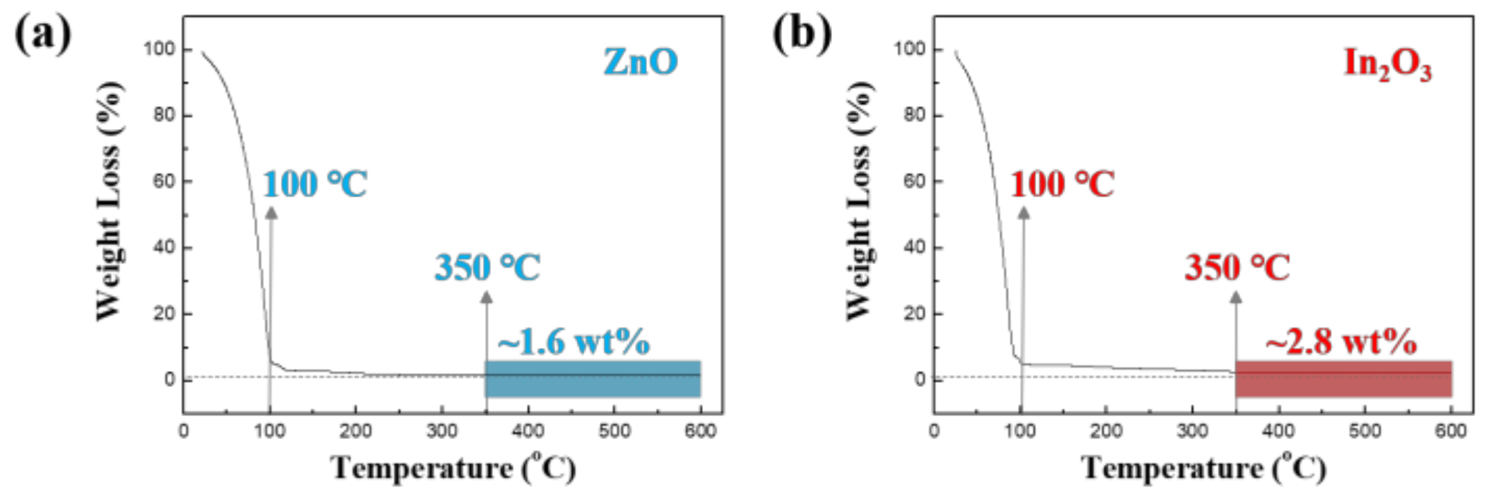
Indium nitrate hydrate (In(NO3)3∙xH2O) (300.83 g/mol, Sigma-Aldrich, St. Louis, MO, USA) and zinc nitrate hydrate (Zn(NO3)2∙xH2O) (189.40 g/mol, Sigma-Aldrich, St. Louis, MO, USA) were used as precursors in this experiment. The precursor solutions were prepared by dissolving In(NO3)3∙xH2O (0.2 M) and Zn(NO3)2∙xH2O (0.1 M) in 2-methoxyethanol (CH3OCH2CHOH) (Sigma-Aldrich, St. Louis, MO, USA). To obtain a homogeneously mixed precursor solution, the prepared solutions were stirred on a hot plate at 75 °C for 6 h by using a magnetic bar. Thermogravimetric analysis (TGA) (N-1000, Sinco, Seoul, Korea) was used to analyze and compare the thermal decomposition processes of the ZnO and In2O3 precursor solutions. The measurement was carried out by raising the temperature from 25 to 600 °C at a heating rate of 10 °C /min in a nitrogen atmosphere. The TGA curves for the precursor solutions prepared in the experiment are shown in Figure 1. We can see that the initial large weight loss (>90%) of the ZnO and In2O3 solutions occurs below 100 °C, this being a result of the evaporation of the solvent and the decomposition of the precursor. In this process, the Zn(NO3)2∙xH2O and In(NO3)3∙xH2O solutions are hydrolyzed to Zn(OH)2 and In(OH)3, respectively. Thereafter, as the temperature continues to rise, the weight loss of both samples gradually slows and becomes constant. This phenomenon is due to the dehydroxylation process of Zn(OH)2 and In(OH)3 to form ZnO and In2O3 [18]; the thermal decomposition of Zn(OH)2 to produce ZnO and H2O takes place at a temperature of 100–250 °C and that of In(OH)3 to produce In2O3 and H2O occurs at 340–850 °C. Furthermore, the weight loss for both precursors is observed to be negligible at temperatures above 350 °C. This indicates that an annealing temperature of 350 °C can be used to convert the precursor solutions into ZnO and In2O3 films.
In this study, solution-processed metal oxide TFTs were fabricated on boron-doped silicon wafers with a 100-nm thermally grown silicon dioxide (SiO2) dielectric layer. To improve the chemical compatibility between the interface of the SiO2 and semiconductor layer, the surface of the cleaned substrate was hydrophilized for 10 s with O2 plasma; a radio frequency power of 40 W was applied with an oxygen flow rate of 9 sccm. For the fabrication of the single-layer In2O3 films, the 0.2 M In2O3 precursor solution was filtered using a 0.2-μm polytetrafluorethylene (PTFE) syringe filter and then spin-coated onto the O2 plasma-treated substrate at 5000 rpm for 35 s. To form the In2O3 semiconductor layer, the spin-coated film was dried on a hotplate at 110 °C for 2 min and then annealed in a furnace at 350 °C for 2 h. For the bilayer case, the ZnO film was first formed on the O2 plasma-treated substrate. In detail, the 0.1 M ZnO precursor solution was filtered through a 0.2-μm PTFE filter and then spin-coated onto the O2 plasma-treated substrates at 4000 rpm. The spin-coated film was dried on a hotplate at 110 °C for 2 min and then annealed at the same temperatures as the In2O3. Subsequently, In2O3 was formed on the ZnO thin film by applying the same process as that used to produce the single-layer In2O3 film. To complete the TFT structure, 40-nm-thick Al source and drain electrodes were thermally deposited onto the semiconductor layer through a shadow mask; the channel width (W) and length (L) were 800 and 50 μm, respectively. Figure 2 shows schematic representations of the bottom-gate/top-contact TFT structures having the In2O3 and ZnO/In2O3 semiconductor layers.
The chemical characteristics of the oxide films were investigated using an X-ray photoelectron spectroscope (K-Alpha, Thermo Scientific, Waltham, MA, USA), and the crystallographic properties were characterized using an X-ray diffractometer (DMAX-2500, Rigaku, Tokyo, Japan). The surface morphologies of the films were examined using a field-emission scanning electron microscope (S-4300, Hitachi, Ibaraki, Japan). The electrical characteristics of the TFTs were evaluated using a semiconductor analyzer (4200-SCS, Keithley, Seoul, Korea).
3. Results and Discussion
Figure 3a–f shows the surface and cross-sectional FE-SEM images of the solution-processed In2O3, ZnO, and ZnO/In2O3 films, respectively. As shown in Figure 3a, the surface of the single-layer In2O3 film exhibits structural defects, such as cracks, voids, and grain boundaries. Figure 3b shows that the distribution of particles on the surface of the ZnO thin film is non-uniform and partially agglomerated. However, such particles on the surface of the underlying ZnO film barely affected the formation of the top layer In2O3 in the bilayer ZnO/In2O3 film. In fact, the surface morphology of the bilayer ZnO/In2O3 film shown in Figure 3c is similar to that of the single-layer In2O3 film shown in Figure 3a. Noteworthy are the grain boundaries in these films. The results suggest that grain boundary effects should be taken into account for analyzing the electrical characteristics of In2O3-based TFTs. From the cross-sectional FE-SEM images in Figure 3d–f, the thicknesses of the In2O3, ZnO, and ZnO/In2O3 films were approximately 22–25 nm, 11–18 nm, and 29–32 nm, respectively.
To investigate the crystallinity of the single-layer In2O3 and bilayer ZnO/In2O3 films, the prepared precursor solutions were spin-coated onto the Si substrates. Figure 4 shows the GIXRD patterns of the Si substrate and the prepared films. By varying the angles of incidence, we found four relatively sharp peaks on the prepared films. This indicates that the single-layer In2O3 and bilayer ZnO/In2O3 films exhibit a polycrystalline structure. Among them, the diffraction peaks appearing at 50–60° in Figure 4a coincide with the Si (100) substrate [19], while the two diffraction peaks appearing at about 30.6 and 35.5° in Figure 4b are the (222) and (400) peaks of In2O3, respectively [20]. The fact that diffraction peaks corresponding to In2O3 in the single- and bilayer films do not change significantly indicates that the crystallinity of the top layer In2O3 is not affected by the underlying ZnO film. However, no diffraction peak of crystalline ZnO is observed in the bilayer film, indicating that the solution-processed ZnO film had an amorphous structure in this study.
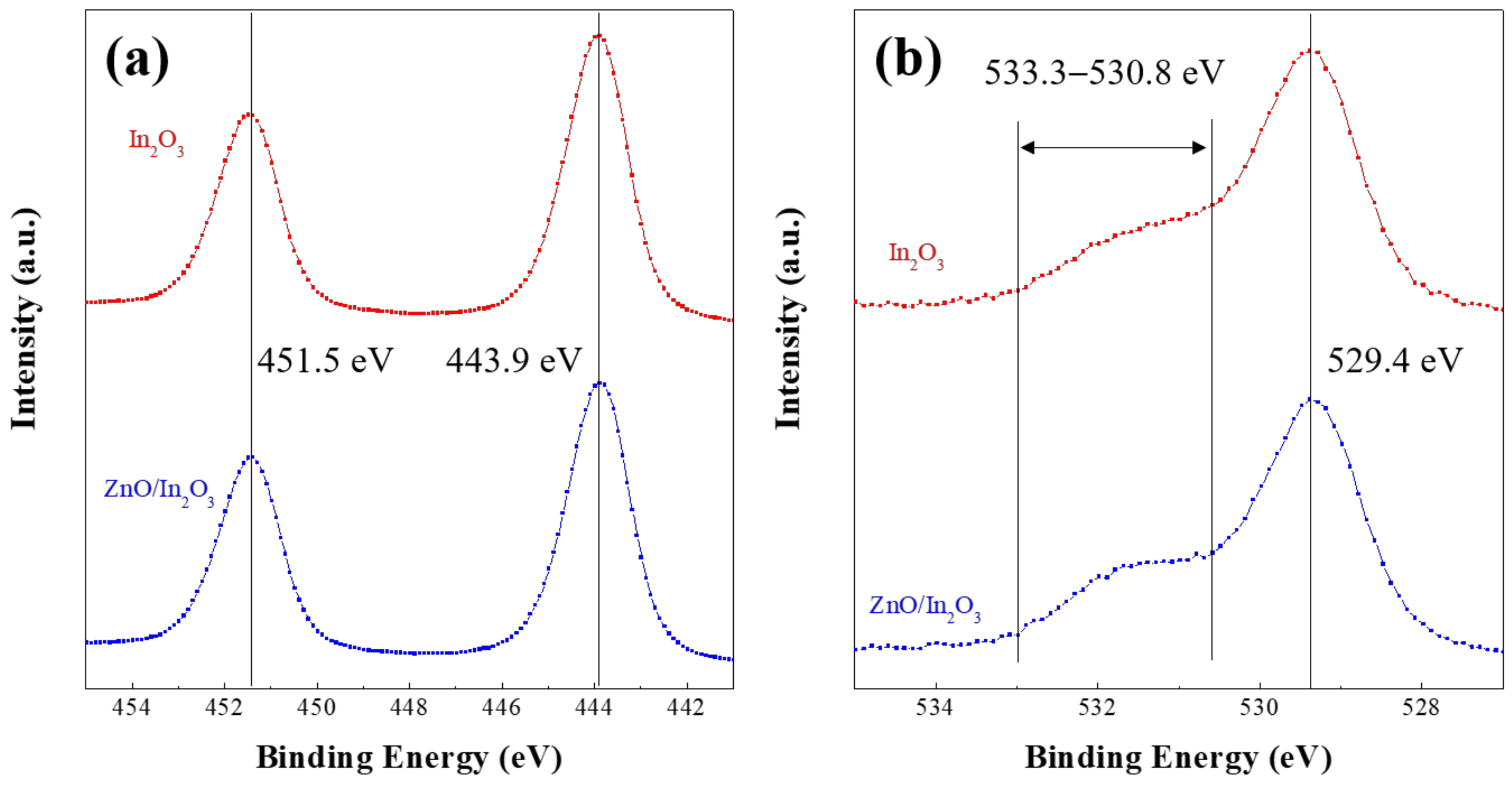
To understand the chemical characteristics of the prepared single- and bilayer films, the surface chemistry and electronic structure of the films were analyzed by using XPS. Figure 5a,b shows the high-resolution XPS spectra of the In 3d and O 1s orbitals in the single-layer In2O3 and bilayer ZnO/In2O3 films, respectively. As shown in Figure 5a, the two binding energy peaks of approximately 451.5 and 443.9 eV in the In 3d XPS spectrum are known to originate from the In 3d3/2 and In 3d5/2 orbitals, respectively [21]. The difference between these two binding energies corresponds to the spin-orbit splitting energy of 7.6 eV, suggesting that the valency of the indium in the film is mainly +3 [22]. We can see that the intensity and binding energy of the In 3d peak of the single- and bilayer do not change significantly. These results indicate that the chemical properties of the In2O3 film are not affected by the underlying ZnO film. Figure 5b shows the high-resolution O 1s XPS peaks of the single-layer In2O3 and bilayer ZnO/In2O3 films. The O 1s peak can be deconvoluted into two peaks in each curve. Among them, the lower binding energy peaks near 529.4 eV are attributed to the lattice oxygen [23,24]. It is known that the shoulders of the spectral region between 530.8 and 533.3 eV originate from the oxygen deficiency and the surface-absorbed oxygen species [23,24]. The comparable XPS results of both films indicate that the distribution of oxygen atoms or ions is not varied by the film structure. Accordingly, the XRD and XPS results confirm that there is no meaningful difference in the crystalline and chemical characteristics of In2O3 between the single-layer In2O3 and bilayer ZnO/In2O3 films.
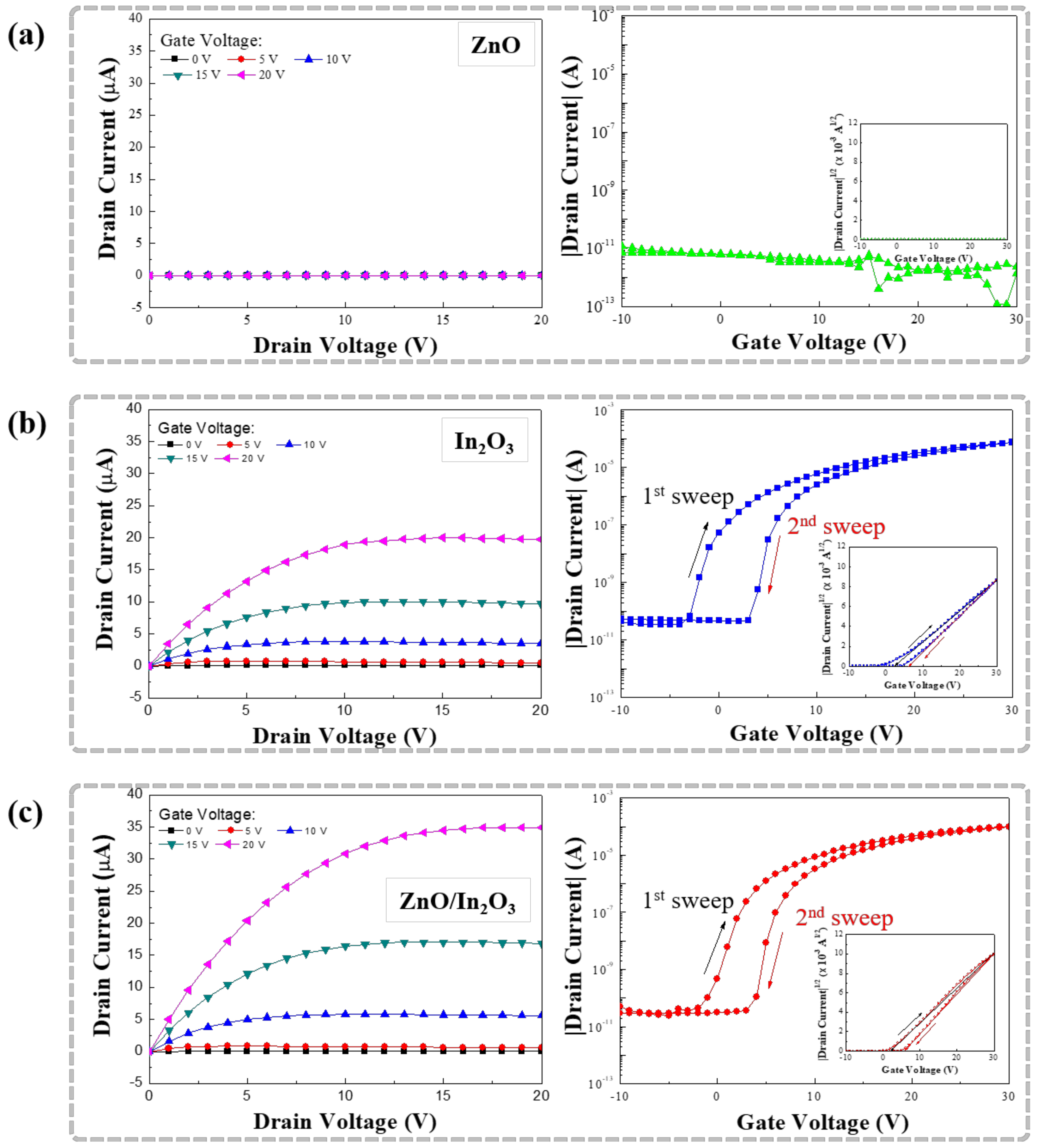
To investigate the difference in the level of performance of the TFTs, the output, transfer, and hysteresis characteristics of the transistors based on the single- and bilayer semiconductors were measured. Figure 6a–c shows the electrical characteristics of the ZnO, In2O3, and ZnO/In2O3 TFTs, respectively. Figure 6a shows that the single-layer ZnO TFT does not function as a TFT, primarily because of the very low thickness (approximately 11–18 nm) of the ZnO semiconductor layer prepared by the solution process. Similar results were found in other experiments upon the preparation of ZnO TFTs by the solution method [10]. On the other hand, the single-layer In2O3 and bilayer ZnO/In2O3 transistors exhibit typical operating characteristics of TFTs as shown in Figure 6b,c. The results indicate that the In2O3 serves as a semiconductor both in the single- and bilayer TFTs. In the measurement of the electrical characteristics of the TFTs, the output characteristics of the prepared TFTs were measured by changing the drain voltage (VD) from 0 to 20 V in increments of 1 V at different constant gate voltages (VG). The value of VG was increased from 0 to 20 V in increments of 5 V. It can be seen from the output characteristic curve that the In2O3 and ZnO/In2O3 TFTs possess excellent saturation characteristics. With the increase in VD, the drain current (ID) increases significantly, indicating that the devices possess significant n-type field-effect characteristics. Additionally, in the case of the bilayer ZnO/In2O3 TFT, the output currents improve under the same measurement conditions. The transfer characteristics were measured at a constant VD of 15 V, while the VG was reversibly swept from −10 to 30 V in increments of 1 V. The on/off current ratios (Ion/Ioff), estimated from the ID–VG curves, were approximately 2.1 × 10⁶ and 3.4 × 10⁶ for the single-layer In2O3 and bilayer ZnO/In2O3 TFTs, respectively. Regarding the performance parameters obtained from the transfer characteristics, the field-effect mobility (μ) in the saturation region can be calculated by the following equation:
where Ci is the capacitance per unit area of the gate dielectric layer and VTH is the threshold voltage. The μ values in the saturation region were approximately 0.3 and 0.5 cm2/Vs for the single- and bilayer TFTs, respectively. The VTH value was also extracted by linear extrapolation of the square root of the ID–VG curve. The VTH value (approximately 1.8 V) of the bilayer ZnO/In2O3 TFT was lower than that (approximately 2.4 V) of the single-layer In2O3 TFT; these values were taken from the transfer characteristics which were firstly measured by sweeping VG from −10 to 30 V. Accordingly, it is confirmed that the bilayer ZnO/In2O3 film contributes to enhancing the TFT performance in terms of drain current, field-effect mobility, and threshold voltage. However, the hysteresis phenomenon in the transfer characteristics of TFTs was not so reduced, even if the bilayer was used. From Figure 6b,c, the clockwise hysteresis is observed in the transfer curves both for the single-layer In2O3 and bilayer ZnO/In2O3 TFTs, which results in a VTH shift (ΔVTH) toward a positive direction upon reversing the VG sweep direction. The obtained ΔVTH values were approximately 3.9 and 3.8 V for the In2O3 and ZnO/In2O3 TFTs, respectively. Since grain boundaries in the solution-processed In2O3 semiconductor layer act as charge-trapping centers during TFT operation [25,26], the comparable ΔVTH values and clockwise hysteresis in our results are due to the polycrystalline nature of In2O3 observed in Figure 3 and Figure 4, not due to the influence of the bilayer structure. Table 1 summarizes the performance parameters of the fabricated TFTs.
Since the crystalline and chemical characteristics of the top In2O3 layer in the bilayer structure are quite comparable to those of the single-layer In2O3 film, the enhancement in the electrical properties of the bilayer ZnO/In2O3 TFT may be explained with the band offset between ZnO and In2O3. Previously, it was reported that, when the vacuum level is set to 0 eV, the valence and conduction bands of In2O3 are positioned at deeper energy levels than those of ZnO [27]. This suggests that the band offset between ZnO and In2O3 may cause charge transport in the bilayer structure. Given that ZnO has a lower Fermi level (approximately 3.2 eV) than that (approximately 4.3 eV) of In2O3 [28,29], it is possible that electrons in the Fermi level of ZnO migrate to that of In2O3 in the bilayer structure, as depicted in Figure 7a. In consequence, the electron migration from ZnO into In2O3 will deplete the electrons near the surface of the underlying ZnO film and then the electron-depletion layer will be positively charged. Such an electron transport phenomenon in the bilayer structure thus forms an internal electric field at the ZnO/In2O3 interface, as shown in Figure 7b. A likely explanation is that the electron migration from the underlying ZnO film increases the carrier concentration in In2O3 and the internal electric field reduces the threshold voltage of the ZnO/In2O3 TFTs by being superimposed on the gate electric field. These behaviors effectively contribute to increasing the drain current and field-effect mobility. Consequently, the enhanced performance of the ZnO/In2O3 TFT can be understood through the electron transport between ZnO and In2O3 and the formation of an internal electric field in the bilayer ZnO/In2O3 structure.
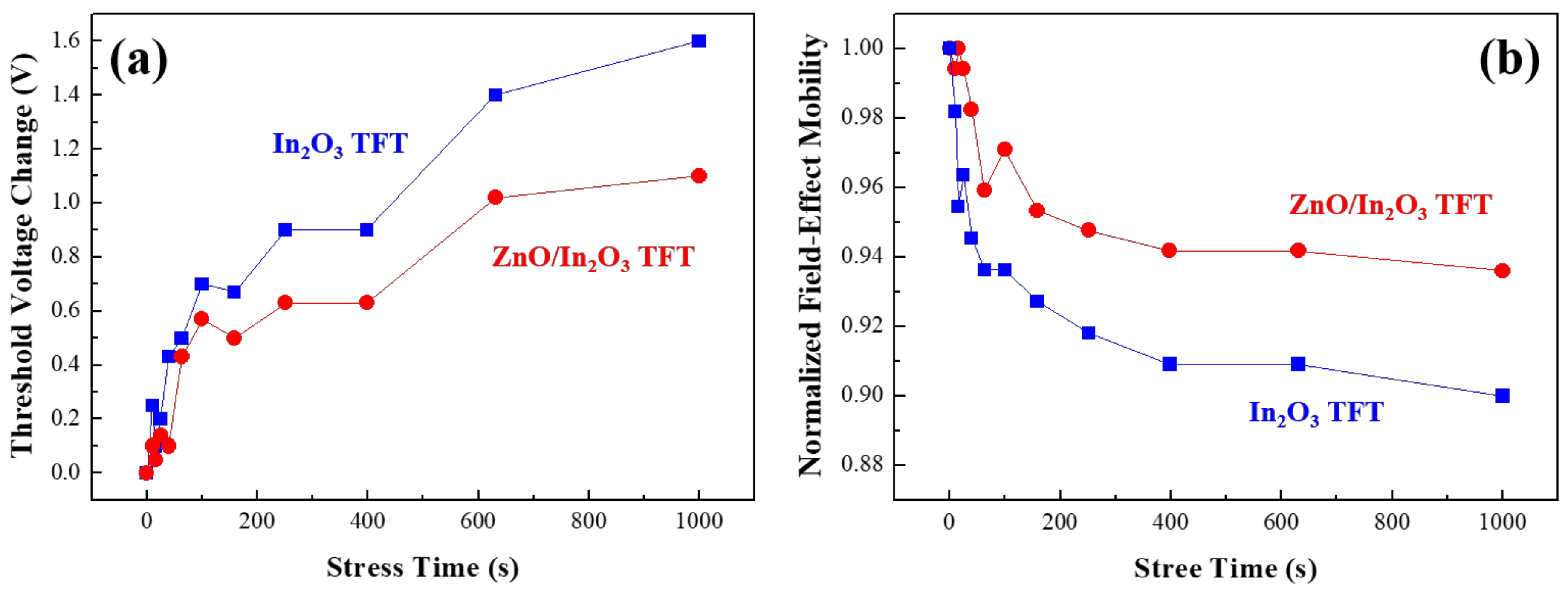
In the literature, it was reported that the time for which TFTs in active-matrix displays are exposed to negative gate bias is more than 500 times longer than that under positive gate bias [30]. Taking into account the significance of negative bias stress, we subjected the single-layer In2O3 and bilayer ZnO/In2O3 TFTs to a negative gate-bias stress. For this experiment, a constant VG of −15 V was applied for an extended time period up to 1000 s, while the source was grounded, and the drain was set at 0 V. After applying a negative gate-bias stress for each stress time, the transfer characteristics of the In2O3 and ZnO/In2O3 TFTs were measured by changing VG from −10 to 30 V in increments of 1 V with VD fixed at 15 V. Figure 8a shows the changes in VTH according to the bias-stress time, which were obtained by subtracting the initial VTH (at stress time = 0 s) from the sequentially measured VTH values. The In2O3 and ZnO/In2O3 TFTs exhibited the positive values of the change in VTH, indicating that VTH was shifted toward a positive direction with proceeding the negative gate-bias stress. The positive shift of VTH can be ascribed to the influence of holes that are trapped in the TFT channel under a prolonged negative gate-bias stress [31,32]. Note that an additional positive voltage should be applied to the gate electrode to form an n-channel after repelling trapped holes, thereby causing a positive shift in VTH. Figure 8b shows the plots of normalized field-effect mobility μ versus bias-stress time; the obtained μ values were normalized with respect to the initial value. Clearly, the μ values of the In2O3 and ZnO/In2O3 TFTs decreased with a negative gate-bias stress. The decrease in μ elucidates that holes, which are trapped in the TFT channel during the negative gate-bias stress, deteriorate the electron transport. The most important observation here is that the positive shift in VTH and the decrease in μ were more pronounced in the single-layer In2O3 TFT than that for the bilayer case. Compared to the results of the single-layer In2O3 TFT, the small changes in VTH and μ of the bilayer ZnO/In2O3 TFT suggest that the internal electric field shown in Figure 7b is effective in reducing the negative gate-bias-induced field and suppressing the trapping of holes in the TFT channel. This explains how the internal electric field induced in the bilayer contributes to the electrical stability of transistors. However, the effects of air molecules on the electrical stability of the fabricated TFTs could not be explored in this study because the transistors were not passivated. To reach a more definite conclusion about the stability issues for the solution-processed bilayer ZnO/In2O3 TFTs, further studies should focus on the environmental stability of the transistors.
4. Conclusions
In summary, the single-layer In2O3 and bilayer ZnO/In2O3 TFTs were fabricated using the sol-gel spin-coating method, and the electrical characteristics of the resulting TFTs were investigated. From the GIXRD and XPS results, the intensity and position of the diffraction peaks related to In2O3 in the bilayer ZnO/In2O3 film were similar to those of the single-layer In2O3 film. This indicates that the underlying ZnO layer does not affect the crystallinity or chemical composition of the top In2O3 layer. In our results, the electrical characteristics of the TFTs were improved by using the bilayer ZnO/In2O3 semiconductor. Considering the energy bands of ZnO and In2O3, the enhancement in the performance of the bilayer TFTs, such as drain current, threshold voltage, and field-effect mobility, could be explained by the electron transport between ZnO and In2O3 and the formation of an internal electric field in the bilayer ZnO/In2O3 structure. In the negative gate-bias stress experiments, we found that the internal electric field helps to improve the electrical stability of the bilayer ZnO/In2O3 TFT by reducing the negative gate-bias-induced field and suppressing the trapping of holes in the TFT channel. However, the clockwise hysteresis and positive threshold voltage shift invariably occurred both in the single-layer In2O3 and bilayer ZnO/In2O3 TFTs owing to the grain boundaries in the In2O3 film. This means that grain boundaries in polycrystalline In2O3 thin films dictate the hysteresis behavior of these TFTs because they can act as trapping centers for mobile charge carriers. Consequently, this study demonstrates that the bilayer structure of solution-processed metal-oxide semiconductors is a viable means of enhancing the TFT performance. Since the rough surface of the underlying ZnO film may cause electron scattering in the TFT channel, we suggest that improving the surface morphology of the underlying ZnO films can further enhance the electrical properties of the solution-processed bilayer TFTs.
Author Contributions
H.L. and X.Z. contributed equally to the fabrication of TFTs, the experimental measurements (TGA characteristics, crystalline and morphological characteristics, and electrical characteristics), and the writing of the manuscript. J.W.K. and E.-J.K. contributed to the analysis of XPS results of the fabricated films. J.P. supervised the whole procedure and contributed to the analysis of the experimental results and the writing of the manuscript. All authors participated in the discussion and commented on the paper.
Funding
This research was supported by Hallym University Research Fund, 2017 (HRF-LGR-2017-0003).
Conflicts of Interest
The authors declare no conflict of interest.
References
- Hoffman, R.L.; Norris, B.J.; Wager, J.F. ZnO-based transparent thin-film transistors. Appl. Phys. Lett. 2003, 82, 733–735. [Google Scholar] [CrossRef]
- Hwang, Y.H.; Seo, J.S.; Yun, J.M.; Park, H.; Yang, S.; Park Ko, S.H.; Bae, B.S. An ‘aqueous route’ for the fabrication of low-temperature-processable oxide flexible transparent thin-film transistors on plastic substrates. NPG Asia Mater. 2013, 5, e45. [Google Scholar] [CrossRef]
- Kim, S.J.; Yoon, S.; Kim, H.J. Review of solution-processed oxide thin-film transistors. Jpn. J. Appl. Phys. 2014, 53, 02BA02. [Google Scholar] [CrossRef]
- Zhang, X.; Lee, H.; Kim, J.; Kim, E.J.; Park, J. Solution-processed gallium–tin-based oxide semiconductors for thin-film transistors. Materials 2017, 11, 46. [Google Scholar] [CrossRef] [PubMed]
- Matsuda, T.; Umeda, K.; Kato, Y.K.; Nishimoto, D.; Furuta, M.; Kimura, M. Rare-metal-free high-performance Ga–Sn–O thin film transistor. Sci. Rep. 2017, 7, 44326. [Google Scholar] [CrossRef] [PubMed]
- Lee, D.H.; Chang, Y.J.; Herman, G.S.; Chang, C.H. A general route to printable high-mobility transparent amorphous oxide semiconductors. Adv. Mater. 2007, 19, 843–847. [Google Scholar] [CrossRef]
- Sheng, J.; Park, E.J.; Shong, B.; Park, J.S. Atomic layer deposition of an indium gallium oxide thin film for thin-film transistor applications. ACS Appl. Mater. Interfaces 2017, 9, 23934–23940. [Google Scholar] [CrossRef] [PubMed]
- Hu, S.; Ning, H.; Lu, K.; Fang, Z.; Li, Y.; Yao, R.; Xu, M.; Wang, L.; Peng, J.; Lu, X. Mobility enhancement in amorphous In–Ga–Zn–O thin-film transistor by induced metallic in nanoparticles and Cu electrodes. Nanomaterials 2018, 8, 197. [Google Scholar] [CrossRef] [PubMed]
- Kumomi, H.; Nomura, K.; Kamiya, T.; Hosono, H. Amorphous oxide channel TFTs. Thin Solid Films 2008, 516, 1516–1522. [Google Scholar] [CrossRef]
- Zhang, X.; Lee, H.; Kwon, J.H.; Kim, E.J.; Park, J. Low-concentration indium doping in solution-processed zinc oxide films for thin-film transistors. Materials 2017, 10, 880. [Google Scholar] [CrossRef] [PubMed]
- Lin, Y.H.; Thomas, S.R.; Faber, H.; Li, R.; McLachlan, M.A.; Patsalas, P.A.; Anthopoulos, T.D. Al-Doped ZnO Transistors Processed from Solution at 120 °C. Adv. Electron. Mater. 2016, 2, 1600070. [Google Scholar] [CrossRef]
- Lee, S.H.; Kim, T.; Lee, J.; Avis, C.; Jang, J. Solution-processed gadolinium doped indium-oxide thin-film transistors with oxide passivation. Appl. Phys. Lett. 2017, 110, 122102. [Google Scholar] [CrossRef]
- Jeong, S.; Lee, J.Y.; Ham, M.H.; Song, K.; Moon, J.; Seo, Y.H.; Ryu, B.H.; Choi, Y. Bendable thin-film transistors based on sol-gel derived amorphous Ga-doped In2O3 semiconductors. Supperlattices Microstruct. 2013, 59, 21–28. [Google Scholar] [CrossRef]
- Chauhan, R.N.; Tiwari, N.; Liu, P.T.; Shieh, H.P.D.; Kumar, J. Silicon induced stability and mobility of indium zinc oxide based bilayer thin film transistors. Appl. Phys. Lett. 2016, 109, 202107. [Google Scholar] [CrossRef]
- Abliz, A.; Huang, C.W.; Wang, J.; Xu, L.; Liao, L.; Xiao, X.; Wu, W.W.; Fan, Z.; Jiang, C.; Li, J.; et al. Rational design of ZnO:H/ZnO bilayer structure for high-performance thin-film transistors. ACS Appl. Mater. Interfaces 2016, 8, 7862–7868. [Google Scholar] [CrossRef] [PubMed]
- Hsu, H.H.; Chang, C.Y.; Cheng, C.H.; Chiou, S.H.; Huang, C.H. High mobility bilayer metal-oxide thin film transistors using titanium-doped InGaZnO. IEEE Electron. Device Lett. 2014, 35, 87–89. [Google Scholar] [CrossRef]
- Yu, X.; Zhou, N.; Smith, J.; Lin, H.; Stallings, K.; Yu, J.; Marks, T.J.; Facchetti, A. Synergistic approach to high-performance oxide thin film transistors using a bilayer channel architecture. ACS Appl. Mater. Interfaces 2013, 5, 7983–7988. [Google Scholar] [CrossRef] [PubMed]
- Li, X.; Li, Q.; Xin, E.; Zhang, J. Sol-gel processed indium zinc oxide thin film and transparent thin-film transistors. J. Sol-Gel Sci. Technol. 2013, 65, 130–134. [Google Scholar] [CrossRef]
- Zhao, L.Y.; Jalili, H.; Panjwani, N.; Chan, T.; He, Z.H.; Heinig, N.F.; Leung, K.T. Formation of ferromagnetic iron core-shell nanocubes on a H-terminated Si(100) surface by electrodeposition. Electrochem. Solid-State Lett. 2007, 10, K47–K49. [Google Scholar] [CrossRef]
- Khan, M.A.M.; Khan, W.; Ahamed, M.; Alhoshan, M. Structural and optical properties of In2O3 nanostructured thin film. Mater. Lett. 2012, 79, 119–121. [Google Scholar] [CrossRef]
- Gurlo, A.; Ivanovskaya, M.; Pfau, A.; Weimar, U.; Göpel, W. Sol-gel prepared In2O3 thin films. Thin Solid Films 1997, 307, 288–293. [Google Scholar] [CrossRef]
- Tetzner, K.; Isakov, I.; Regoutz, A.; Payne, D.J.; Anthopoulos, T.D. The impact of post-deposition annealing on the performance of solution-processed single layer In2O3 and isotype In2O3/ZnO heterojunction transistors. J. Mater. Chem. C 2017, 5, 59–64. [Google Scholar] [CrossRef]
- Lee, H.; Zhang, X.; Hwang, J.; Park, J. Morphological influence of solution-processed zinc oxide films on electrical characteristics of thin-film transistors. Materials 2016, 9, 851. [Google Scholar] [CrossRef] [PubMed]
- Nayak, P.K.; Hedhili, M.N.; Cha, D.; Alshareef, H.N. High performance In2O3 thin film transistors using chemically derived aluminum oxide dielectric. Appl. Phys. Lett. 2013, 103, 033518. [Google Scholar] [CrossRef]
- Leoppäniemi, J.; Huttunen, O.-H.; Majumdar, H.; Alastalo, A. Flexography-printed In2O3 semiconductor layers for high-mobility thin-film transistors on flexible plastic substrate. Adv. Mater. 2015, 27, 7168–7175. [Google Scholar] [CrossRef]
- Gupta, D.; Anand, M.; Ryu, S.W.; Choi, Y.K.; You, S. Nonvolatile memory based on sol-gel ZnO thin-film transistors with Ag nanoparticles embedded in the ZnO/gate insulator interface. Appl. Phys. Lett. 2008, 93, 224106. [Google Scholar] [CrossRef]
- Ganose, A.M.; Scanlon, D.O. Band gap and work function tailoring of SnO2 for improved transparent conducting ability in photovoltaics. J. Mater. Chem. C 2016, 4, 1467–1475. [Google Scholar] [CrossRef]
- Lang, O.; Pettenkofer, C.; Sánchez-Royo, J.F.; Segura, A.; Klein, A.; Jaegermann, W. Thin film growth and band lineup of In2O3 on the layered semiconductor InSe. J. Appl. Phys. 1999, 86, 5687. [Google Scholar] [CrossRef]
- Dearden, C.A.; Walker, M.; Beaumont, N.; Hancox, I.; Unsworth, N.K.; Sullivan, P.; McConville, C.F.; Jones, T.S. High voltage hybrid organic photovoltaics using a zinc oxide acceptor and a subphthalocyanine donor. Phys. Chem. Chem. Phys. 2014, 16, 18926–18932. [Google Scholar] [CrossRef] [PubMed] [Green Version]
- Conley, J.F. Instabilities in amorphous oxide semiconductor thin-film transistors. IEEE Trans. Device Mater. Reliab. 2010, 10, 460–475. [Google Scholar] [CrossRef]
- Mathews, W.P.; Vemuri, R.N.P.; Alford, T.L. Influence of extended bias stress on the electrical parameters of mixed oxide thin film transistors. Circuits Syst. 2012, 3, 295–299. [Google Scholar] [CrossRef]
- Zhang, X.; Ndabakuranye, J.P.; Kim, D.W.; Choi, J.S.; Park, J. Stability study of solution-processed zinc tin oxide thin-film transistors. Electron. Mater. Lett. 2015, 11, 964–972. [Google Scholar] [CrossRef]
Figure 1.
Thermogravimetric analysis (TGA) curves of (a) ZnO and (b) In2O3 precursor solutions.

Figure 2.
(a) Single-layer In2O3 thin-film transistor (TFT) and (b) bilayer ZnO/In2O3 TFT.

Figure 3.
Surface and cross-sectional field-emission scanning electron microscopy (FE-SEM) images of the single-layer (a,d) In2O3 and (b,e) ZnO films, and (c,f) bilayer ZnO/In2O3 film.
Figure 3.
Surface and cross-sectional field-emission scanning electron microscopy (FE-SEM) images of the single-layer (a,d) In2O3 and (b,e) ZnO films, and (c,f) bilayer ZnO/In2O3 film.

Figure 4.
Grazing incidence X-ray diffraction patterns (GIXRD) patterns of (a) Si wafer; (b) single-layer In2O3, and bilayer ZnO/In2O3 films.
Figure 4.
Grazing incidence X-ray diffraction patterns (GIXRD) patterns of (a) Si wafer; (b) single-layer In2O3, and bilayer ZnO/In2O3 films.

Figure 5.
High-resolution X-ray photoemission spectroscopy (XPS) spectra of (a) In 3d and (b) O 1s orbitals in the single-layer In2O3 and bilayer In2O3/ZnO.
Figure 5.
High-resolution X-ray photoemission spectroscopy (XPS) spectra of (a) In 3d and (b) O 1s orbitals in the single-layer In2O3 and bilayer In2O3/ZnO.

Figure 6.
Electrical characteristics of TFTs fabricated with the (a) ZnO; (b) In2O3 and (c) ZnO/In2O3.
Figure 6.
Electrical characteristics of TFTs fabricated with the (a) ZnO; (b) In2O3 and (c) ZnO/In2O3.

Figure 7.
(a) Energy band structures of ZnO and In2O3 and (b) Description of internal electric field induced at the ZnO/In2O3 interface.
Figure 7.
(a) Energy band structures of ZnO and In2O3 and (b) Description of internal electric field induced at the ZnO/In2O3 interface.

Figure 8.
Variations in (a) threshold voltage and (b) field-effect mobility of the In2O3 and ZnO/In2O3 TFTs as a result of negative gate-bias stress.
Figure 8.
Variations in (a) threshold voltage and (b) field-effect mobility of the In2O3 and ZnO/In2O3 TFTs as a result of negative gate-bias stress.


Table 1.
Performance parameters of the fabricated TFTs.
| TFT | Threshold Voltage (V) | Mobility (cm2/Vs) | Ion/Ioff | △VTH (V) |
|---|---|---|---|---|
| ZnO | - | - | - | - |
| In2O3 | 2.4 ± 0.1 | 0.3 ± 0.1 | 2.1 × 10⁶ | 3.9 |
| ZnO/In2O3 | 1.8 ± 0.2 | 0.5 ± 0.1 | 3.4 × 10⁶ | 3.8 |
© 2018 by the authors. Licensee MDPI, Basel, Switzerland. This article is an open access article distributed under the terms and conditions of the Creative Commons Attribution (CC BY) license (http://creativecommons.org/licenses/by/4.0/).
Share and Cite
MDPI and ACS Style
Lee, H.; Zhang, X.; Kim, J.W.; Kim, E.-J.; Park, J. Investigation of the Electrical Characteristics of Bilayer ZnO/In2O3 Thin-Film Transistors Fabricated by Solution Processing. Materials 2018, 11, 2103. https://doi.org/10.3390/ma11112103
AMA Style
Lee H, Zhang X, Kim JW, Kim E-J, Park J. Investigation of the Electrical Characteristics of Bilayer ZnO/In2O3 Thin-Film Transistors Fabricated by Solution Processing. Materials. 2018; 11(11):2103. https://doi.org/10.3390/ma11112103
Chicago/Turabian StyleLee, Hyeonju, Xue Zhang, Jung Won Kim, Eui-Jik Kim, and Jaehoon Park. 2018. "Investigation of the Electrical Characteristics of Bilayer ZnO/In2O3 Thin-Film Transistors Fabricated by Solution Processing" Materials 11, no. 11: 2103. https://doi.org/10.3390/ma11112103
Note that from the first issue of 2016, this journal uses article numbers instead of page numbers. See further details here.