Article

Wafer-Scale Hierarchical Nanopillar Arrays Based on Au Masks and Reactive Ion Etching for Effective 3D SERS Substrate

Jiangxi Key Laboratory of Surface Engineering, Jiangxi Science and Technology Normal University, Nanchang 330013, China
*
Author to whom correspondence should be addressed.
Materials 2018, 11(2), 239; https://doi.org/10.3390/ma11020239
Submission received: 10 January 2018 / Revised: 27 January 2018 / Accepted: 29 January 2018 / Published: 4 February 2018

Abstract

:
Two-dimensional (2D) periodic micro/nanostructured arrays as SERS substrates have attracted intense attention due to their excellent uniformity and good stability. In this work, periodic hierarchical SiO2 nanopillar arrays decorated with Ag nanoparticles (NPs) with clean surface were prepared on a wafer-scale using monolayer Au NP arrays as masks, followed by reactive ion etching (RIE), depositing Ag layer and annealing. For the prepared SiO2 nanopillar arrays decorated with Ag NPs, the size of Ag NPs was tuned from ca. 24 to 126 nanometers by controlling the deposition thickness of Ag film. Importantly, the SiO2 nanopillar arrays decorated with Ag NPs could be used as highly sensitive SERS substrate for the detection of 4-aminothiophenol (4-ATP) and rhodamine 6G (R6G) due to the high loading of Ag NPs and a very uniform morphology. With a deposition thickness of Ag layer of 30 nm, the SiO2 nanopillar arrays decorated with Ag NPs exhibited the best sensitive SERS activity. The excellent SERS performance of this substrate is mainly attributed to high-density “hotspots” derived from nanogaps between Ag NPs. Furthermore, this strategy might be extended to synthesize other nanostructured arrays with a large area, which are difficult to be prepared only via conventional wet-chemical or physical methods.

Graphical Abstract

1. Introduction

Surface enhanced Raman scattering (SERS) has been considered as a promising spectroscopic technique for label-free and nondestructive trace detection for biological and chemical analytes at super low concentration with ultra-sensitivity [1,2,3,4,5,6,7]. The Raman scattering signals of the analytes adsorbed on a rough surface of plasmonic metals could be amplified by several orders of magnitude [8,9,10,11]. Noble metal (Au and Ag) nanoparticles (NPs) can generate intense electromagnetic field due to localized surface plasmon resonance (LSPR), resulting in excellent activity as a SERS substrate [9]. The places where the electromagnetic field is extremely strong for enhancing Raman scattering are called “hotspots”, which mainly depend on the nanogap, morphology, size and nature of the metal materials [12]. In recent decades, significant efforts have been raised to construct SERS substrates by synthesizing Au, Ag and Au–Ag alloyed NPs with different size and morphologies, such as concave trisoctahedral and calyptriform Au nanocrystal [13], porous Au NPs [14], porous Au–Ag alloyed nanocubes [15], Ag–Au hybrid nanosponges [16] and AuAg bimetallic nanoparticles [17]. For example, Gao and co-workers fabricated porous Au–Ag alloy NPs with clean surface via a dealloying process. The high porosity of theses Au–Ag alloyed NPs can produce abundant inherent “hotspots” and the clean surfaces make these “hotspots” readily accessible for target molecules. These conditions make the producing Au–Ag alloyed NPs show excellent SERS activity [18].
The uniformity and reproducibility of the SERS substrate should also be improved in addition to the activity of the SERS substrate. Two-dimensional (2D) periodic micro/nanostructured arrays using as SERS substrates have attracted intense attention due to their excellent uniformity and good stability [19,20,21,22,23]. This kind of SERS substrates was mainly constructed using monolayer colloidal crystals as template, followed by solution-dipping or electrochemical deposition technique [20,21,22,23]. For instance, Meng and co-workers fabricated hierarchical periodic Ag nanorod bundles arrays as SERS substrates with good uniformity and reproducibility. The Ag nanorod bundles arrays were constructed by using 2D ordered anodic aluminum oxide (AAO) membrane and polystyrene (PS) nanosphere array as a dual template, followed by electrodepositing. In each bundle, “hot spots” are generated between adjacent Ag nanorods after solution evaporation, leading to the SERS sensor with high sensitivity [23]. However, although these methods have the advantages of low costs, they need complex and strict preparation procedure. Additionally, these fabrication methods suffer from significantly low production yield as only a small area array is fabricated in each process, which seriously hinders their further practical applications. Over the past decade, many significant efforts have been devoted to maximizing the sensitivity of these substrates rather than addressing the issue of expanding the area. Nevertheless, for practical applications it remains highly desirable to prepare SERS substrates with a large area.
In this work, a facile method has been presented to fabricate 2D SiO2 nanopillars decorated with Ag NPs arrays as SERS substrates in a large area with a well-controllable morphology. The 2D SiO2 nanopillar array was prepared using 2D Au NPs arrays as a template combined with reactive ion etching (RIE). After depositing a layer of Ag on the as-prepared SiO2 nanopillar array, it was annealed at 600 °C for 2 h to form 2D SiO2 nanopillar arrays decorated with Ag NPs. The area of as-obtained arrays can achieve wafer-scale with a very uniform morphology. Importantly, after depositing 30 nm Au layer, the SiO2 nanopillar decorated with Ag NPs array could be used as highly sensitive SERS substrates for the detection of 4-aminothiophenol (4-ATP) and rhodamine 6G (R6G). By effectively controlling the deposition thickness of Ag layer, the size of Ag NPs could be tuned from ca. 24 to 126 nm. When the deposition thickness of Ag layer is 30 nm, the SiO2 nanopillar arrays decorated with Ag NPs possess highly sensitive SERS activity. The excellent SERS performance of this substrate is mainly attributed to high-density “hotspots” derived from nanogaps between Ag NPs. Furthermore, this strategy might be extended to synthesize other nanostructures with a large area, which are difficult to be prepared only via conventional wet-chemical or physical methods.

2. Materials and Methods

2.1. Materials

Polystyrene (PS) microspheres suspension (2.50 wt. % in water, 500 nm in diameter) was purchased from Alfa Aesar Corporation (Heysham, UK). The reagents including ethanol, acetone, H2SO4 and NH3.H2O were bought from Sinopharm Chemical Reagent Co., Ltd. (Shanghai, China). 4-ATP and R6G were obtained from Aladdin Industrial Corporation (Hangzhou, China). SiO2 substrate was offered by TRION Technology Corporation (Tempe, AZ, USA). The targets of pure Au and Ag (99.99%) were bought from ZhongNuo Advanced Material Technology Corporation (Beijing, China). Deionized water was prepared with a Milli-Q water purification system (Merck, Darmstadt, Germany). All the chemicals were of analytical grade and were used without further purification.

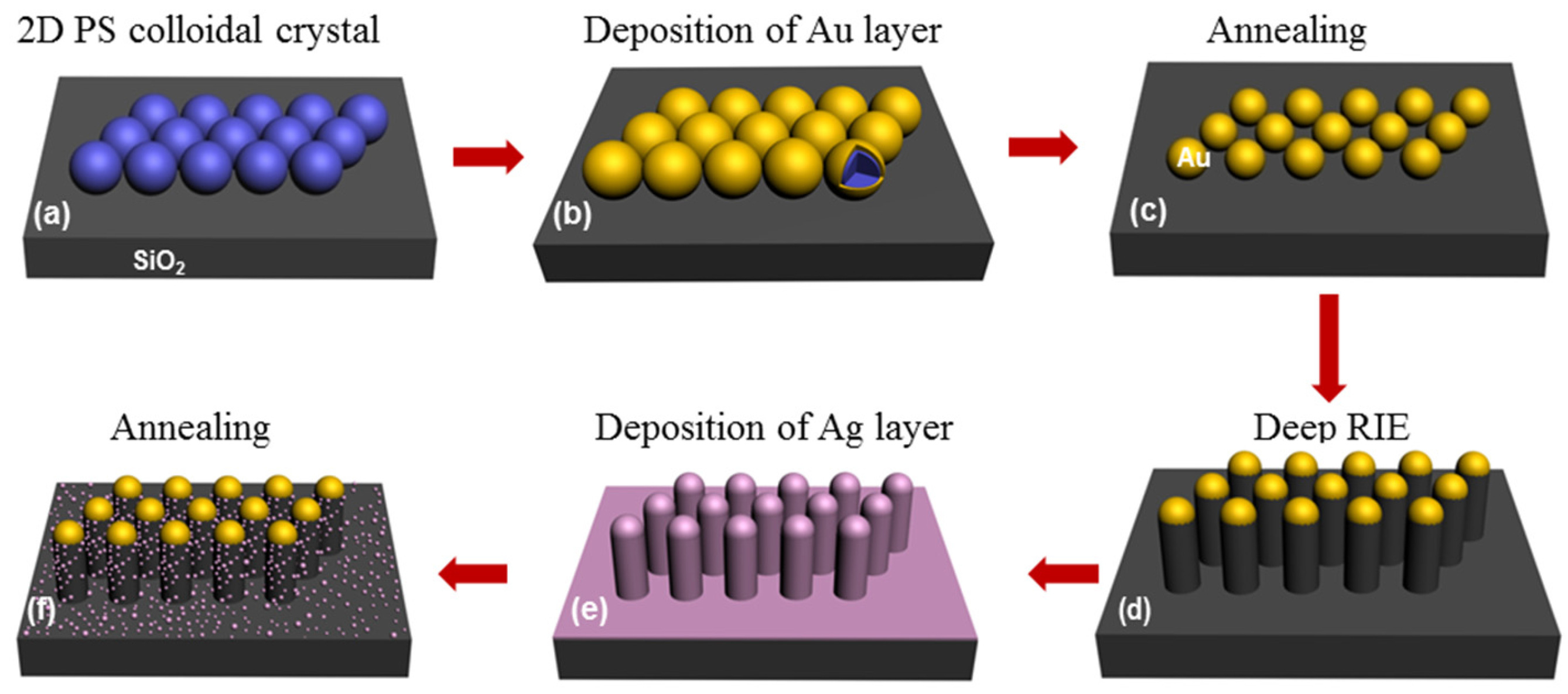
2.2. Fabrication of the SiO2 Nanopillar Arrays Decorated with Ag NPs

The hierarchical SiO2 nanopillar arrays decorated with Ag NPs @ Au film were fabricated as following process (Figure 1). Briefly, 2D Au NPs arrays with hexagonal non-close-packed (HNCP) arrangement on SiO2 substrate was fabricated by using the 2D PS colloidal crystal as a template and further annealing, as previously reported (Figure 1a–c) [24,25]. Subsequently, the as-prepared 2D Au NPs arrays on the SiO2 substrate with the periodic length of 500 nm and diameter of 260 nm as a mask was put into the RIE chamber (Sirus T2, TRION Technology, Clearwater, FL, USA) for etching (Figure 1d). During the RIE process, etching-reactive gases CHF3 and O2 were introduced into the chamber with a flow of 46 and 4 sccm, under the pressure at 120 mTorr, etching power of 150 W and etching time for 1500 s, respectively. The SiO2 nanopillar arrays were fabricated in this process. After that, a layer of Ag was deposited on the as-formed SiO2 nanopillar arrays by an ion-beam coater with a sputtering current of 20 mA under different deposition time. To make the Ag film disperse evenly on the surfaces of the nanopillars, during the depositing process of Ag layer, the samples were placed at 45° for the first deposition and then rotated about 90° along the normal of sample for further depositing with the same parameters until return to original position. The thickness of Ag layer was tuned by deposition time. Then, the SiO2 nanopillar arrays with deposited Ag layer was calcined at 600 °C for 2 h to form the SiO2 nanopillar arrays decorated with Ag NPs. Finally, 30 nm Au film was deposited on the as-prepared SiO2 nanopillar arrays decorated with Ag NPs before further SERS measurement.

2.3. Characterization

The morphologies of as-prepared samples were characterized by a field-emission scanning electron microscope (FE-SEM, Sirion200, FEI, Hillsboro, OR, USA). 4-ATP and R6G were used as a probe molecule to evaluate the SERS performance of the as-fabricated active substrates. SERS measurements were conducted by a confocal microprobe Raman spectrometer (Reni Shaw inVia Reflex, London, UK) with a laser beam of 532 nm wavelength. The laser operated at 5 mW and the integral time was 9 s. Before SERS measurements, the as-fabricated active substrates were immersed in 10 mL 4-ATP alcoholic solution or R6G aqueous solution with different concentrations for 30 min, cleaned with deionized water several times, and then dried in a flow of nitrogen. For comparison, all the samples share the same condition of adsorption and measurement of Raman spectrum.

3. Results and Discussion

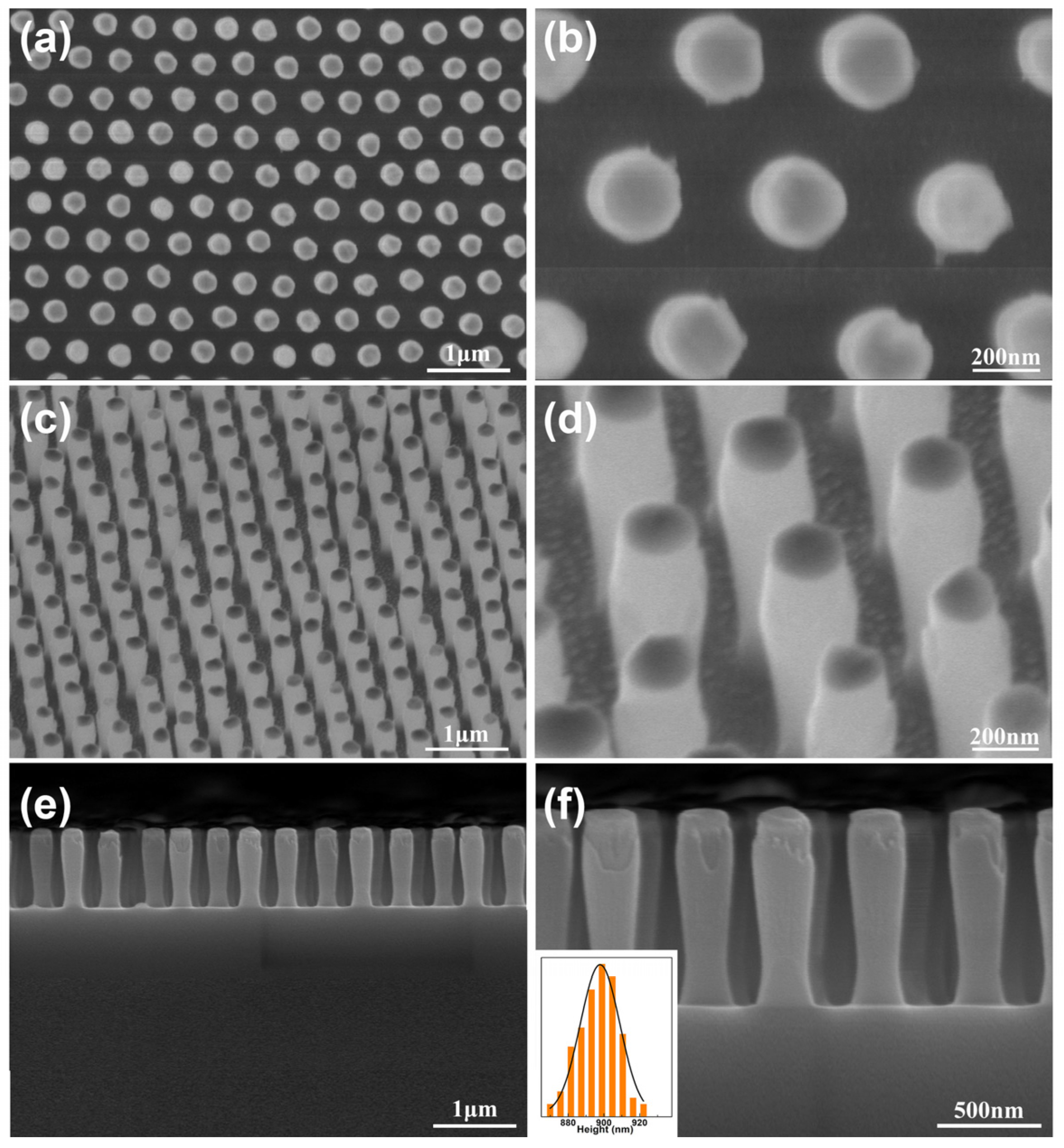
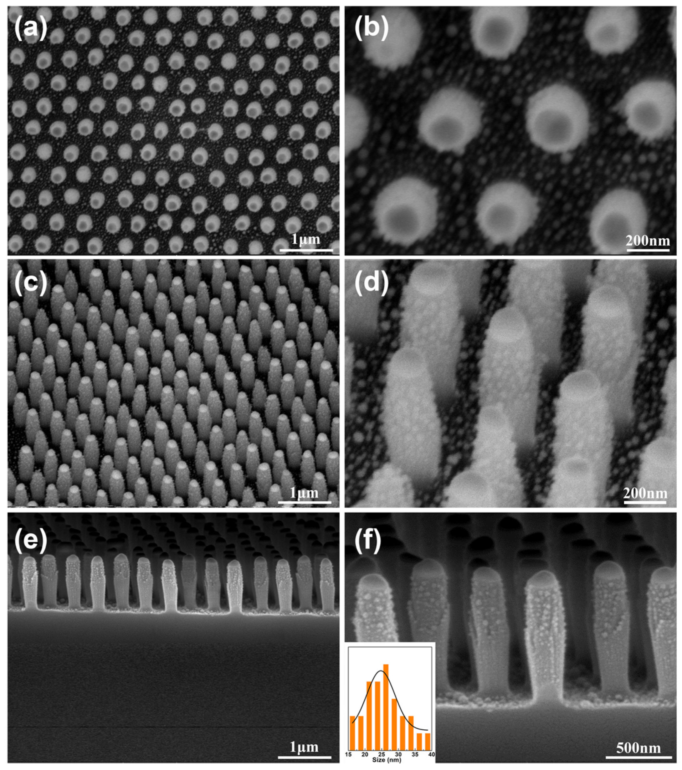
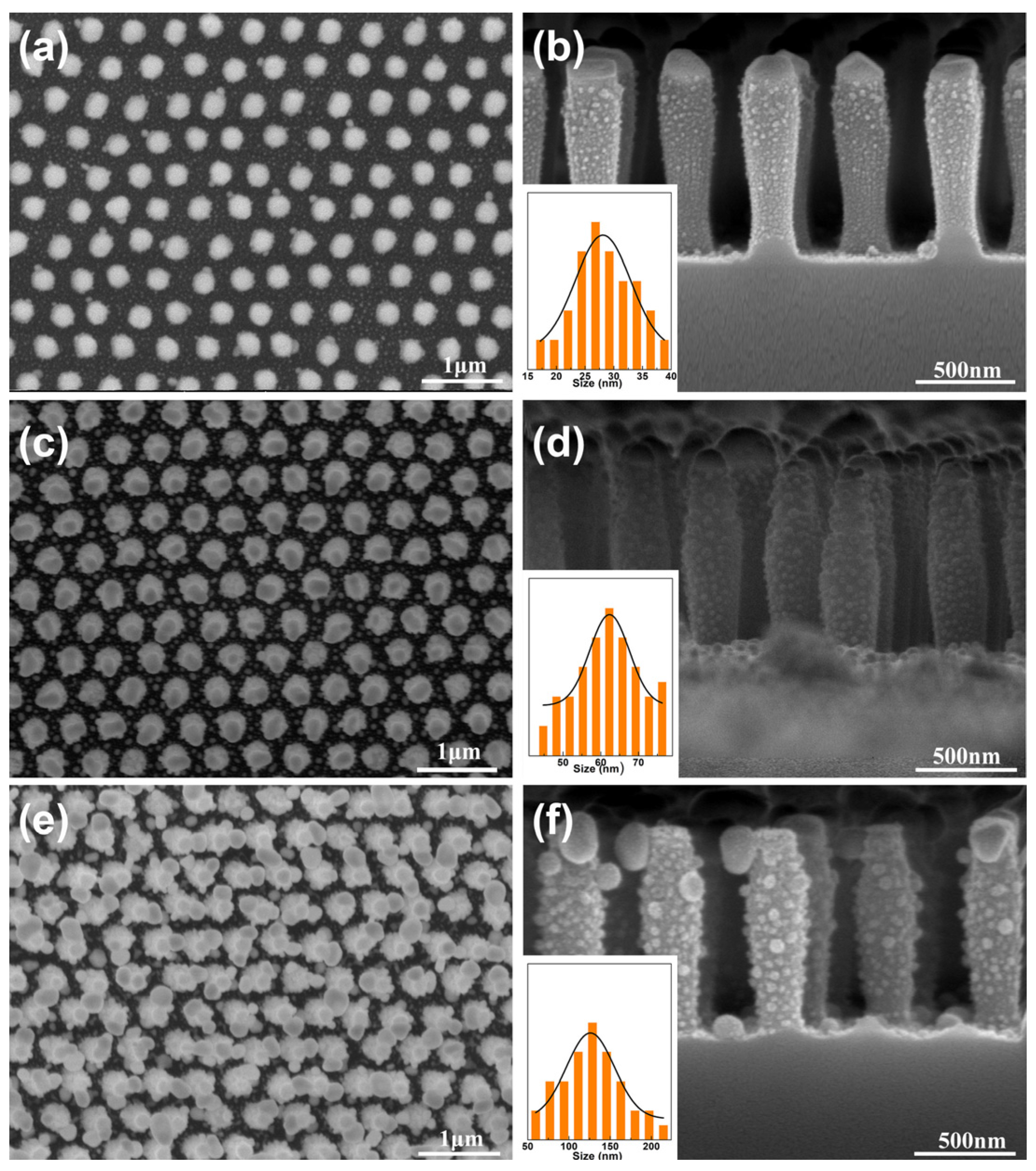
3.1. The SiO2 Nanopillar Arrays

Ordered SiO2 nanopillar arrays were formed under a certain etching power (150 W), etching pressure (120 mTorr) by using monolayer Au NP arrays as masks. Figure 2 displays the FE-SEM images of the SiO2 nanopillar arrays under etching time of 1500 s. From the top-view SEM images, it is apparent that all of the nanopillars are arranged in an ordered HNCP alignment with a periodicity of 500 nm (Figure 2a). The diameter of each structural unit is ca. 220 nm (Figure 2b). Each structural unit has a nanopillar-shape (Figure 2c). There is an Au NP on the top of each nanopillar (Figure 2d), resulting from the residue of the mask. The height of the SiO2 nanopillar is ca. 898 nm (Figure 2e,f). Additionally, the diameter of lower half of the nanopillar is slightly smaller than that of the upper part, mainly due to the effect of isotropic etching. The longitudinal etching also occurs at different degrees in the etching process. A detailed statement about device and mechanism of RIE was reported in our previous work [19].

3.2. The Hierarchical SiO2 Nanopillar Decorated with Ag NPs Arrays

To decorate SiO2 nanopillar array with Ag NPs, an Ag layer with a certain thickness was deposited onto the top and sidewall of the as-prepared SiO2 nanopillar arrays by magnetron sputtering deposition technology. The periodic SiO2 nanopillar arrays decorated with Ag NPs were obtained by annealing the SiO2 nanopillar array with Ag coating in a furnace at 600 °C for 2 h. The morphology of Ag NPs can be tuned by the deposition thickness of the Ag layer. As observed in Figure 3, the Ag NPs were successfully synthesized on the nanopillars. The regularity and interspacing of the array exhibit no significant change, as shown in Figure 3a,b. The distribution of the Ag NPs on the surface of the SiO2 nanopillars with a size of ca. 24 nm is disorderly (Figure 3c,d). Additionally, as shown in Figure 3e,f, the bottom region of the nanopillars also contains a large number of Ag NPs, and the Au NPs as a mask were transformed into discal Au NPs. Meanwhile, elemental mapping images of the SiO2 nanopillar array decorated with Ag NPs (Supplementary Materials, Figure S1) revealed the existence of Si, O and Ag elements dispersed in the position of nanopillars and the bottom region with SiO2 being a majority. The Au element mainly dispersed on the top of nanopillars. Further studies show that Ag element also appeared at the top of nanopillars, indicating that Au–Ag alloy NPs formed. Additionally, in Figure 3f, it can be seen that there are no obvious Ag NPs presenting on the surfaces of the discal Au NPs. This case was attributed to the depositing Ag film in this region being melted with Au NPs to form Au–Ag alloy NPs, which was consistent with elemental mapping image. Moreover, the size of Ag NPs in the upper part of the nanopillar is larger than that in the lower part (Figure 3f). The reason is likely to be that Ag atoms (group) from the multiple directions at the top of nanopillars would be blocked by approaching nanopillars, resulting in a thicker Ag film in upper part of nanopillar than in the bottom half due to the multidirectional deposition and shadow effect in the process of sputtering deposition.
Apart from the above-mentioned deposition thickness of Ag layer with 20 nm, four additional samples with the 30 nm, 60 nm and 90 nm thickness of deposited Ag layer have also been prepared. The morphology of the sample changes gradually with the increase of the thickness of Ag layer. When the thickness increased to 30 nm, the hierarchical SiO2 nanopillar arrays decorated with Ag NPs has a similar morphology as that of 20 nm, as shown in Figure 4a,b. If the deposition thickness of Ag layer increased to 60 nm, the size of Ag NPs increased to ca. 62 nm, as shown in Figure 4c,d. However, if the thickness further increased to 90 nm, the morphology of the sample would change greatly, as shown in Figure 4e,f. The periodicity of the structural array was destroyed and the size of the Ag NPs reached up to ca. 126 nm, making the adjacent structural units link together. Subsequently, the hierarchical periodic arrays composed of SiO2 nanopillar arrays decorated with Ag NPs with deposition thickness of 20 nm, 30 nm, 60 nm and 90 nm were selected for further SERS investigation. A rough surface is important to increase the SERS signals [21]. To increase the surface roughness, 30 nm Au layer was deposited on the as-prepared SiO2 nanopillar arrays decorated with Ag NPs before further SERS measurement. A comparison of Au–Ag alloy NP before and after depositing Au film was studied, as shown in Figure S2 (Supplementary Materials). In Figure S2, it can be seen that the surface became rougher after depositing Au film.

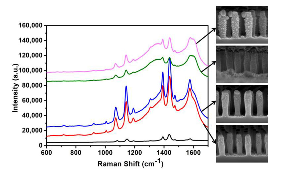
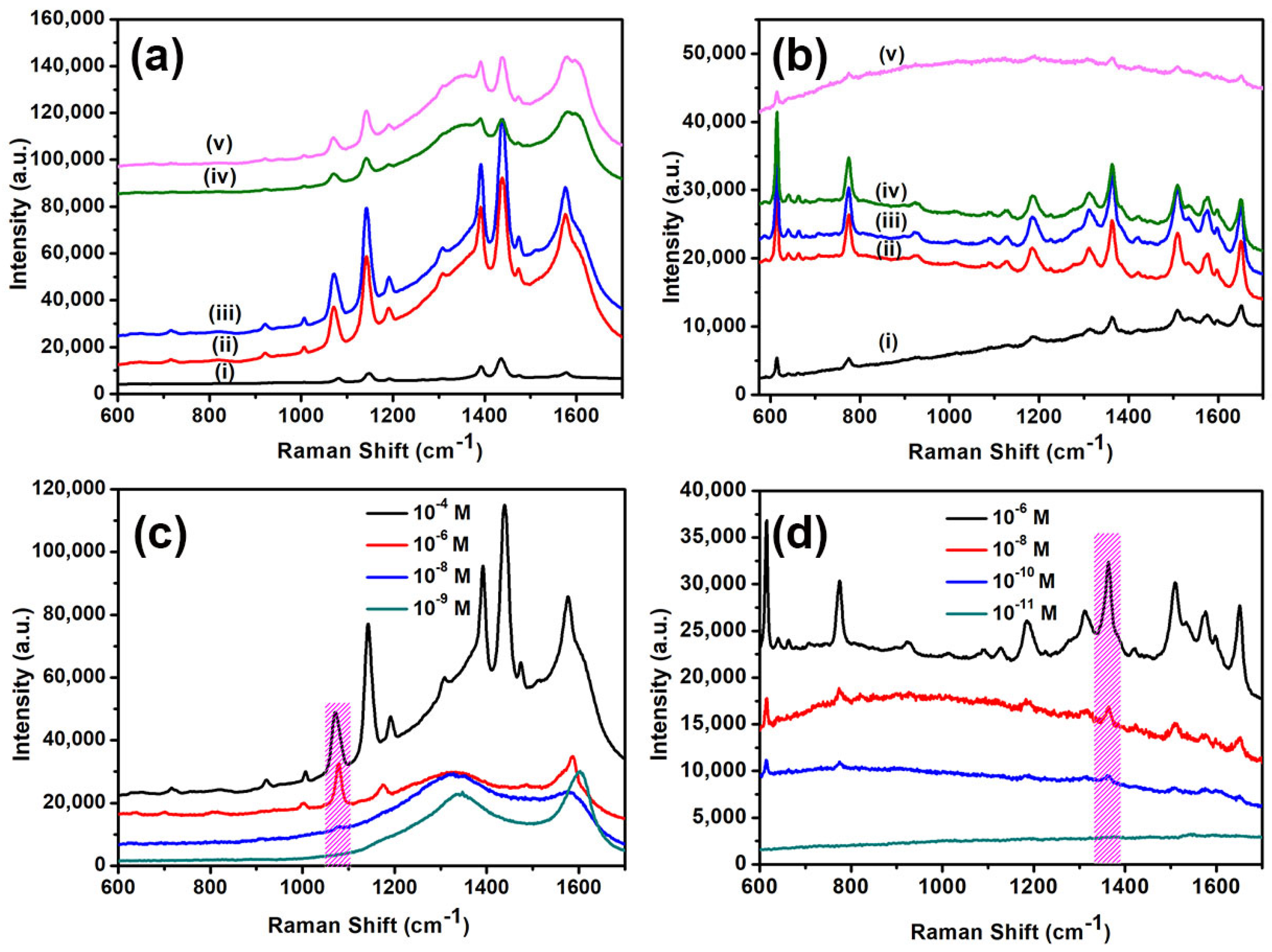
3.3. SERS Enhancement of Hierarchical SiO2 Nanopillar Arrays Decorated with Ag NPs

In this work, 4-ATP was used as a molecule to evaluate enhancement of Raman signals of the as-prepared SERS active substrates. Raman spectra of 10−4 M 4-ATP on the SiO2 nanopillars array, SiO2 nanopillars with the Ag film, SiO2 nanopillar arrays decorated with Ag NPs and SiO2 nanopillar arrays decorated with Ag NPs after depositing Au film are shown in Figure S3 (Supplementary Materials). Compared with the SiO2 nanopillars, the Raman signal intensity of SiO2 nanopillars with the Ag film was enhanced. This enhancement can be attributed to increase surface roughness arising from depositing Au layer. Furthermore, when the Ag layer deposited on SiO2 nanopillars was changed into Ag NPs by annealing treatment, the SERS signals rapid declined, because the surfaces of these Ag NPs became smooth. However, when a layer of Au film was deposited onto the SiO2 nanopillar arrays decorated with Ag NPs, the SERS signals was considerably enhanced due to increasing surface roughness. Compared with the SiO2 nanopillar arrays with Ag film, the Raman signal intensity (1080 cm−1 for 4-ATP) of SiO2 nanopillar array decorated with Ag NPs after depositing Au film was considerably enhanced and increased ca. 7 times. This case was mainly attributed to the increasing number of “hotspots” originated from the Ag NPs on the SiO2 nanopillars. The as-prepared hierarchical SiO2 nanopillar array decorated with Ag NPs @ Au film possess rough surface and abundant SERS “hotspots”, and they could be used as a SERS-active substrate.
Raman spectra of the 10−4 M 4-ATP on substrates with different morphologies is shown in Figure 5. All samples were immersed in 10−4 M 4-ATP solution for 30 min and dried in air before detection. A SiO2 wafer with a flat surface-coated 30 nm Au film served as the reference sample and its Raman spectra was observed in Curve (i) of Figure 5a. The other four curves in Figure 5 from bottom to top correspond to Raman spectra of the substrates with different deposition thickness of Ag layer before annealing: 20 nm (ii); 30 nm (iii); 60 nm (iv); and 90 nm (v). As shown in Figure 5a, the obtained hierarchical SiO2 nanopillar arrays decorated with Ag NPs after depositing 30 nm Au film reveal obvious SERS enhancements compared with the reference sample. The peak intensity slightly increased with increasing deposition thickness below 30 nm, but decreased when the deposition thickness exceeded 30 nm. Beside 4-ATP, the hierarchical SiO2 nanopillar arrays decorated with Ag NPs exhibited good SERS performance for R6G. The similar tendency was observed as 4-ATP when 10−6 M R6G was detected under different morphologies, as shown in Figure 5b. Hence, the as-prepared periodic arrays achieved the optimal SERS activity at the deposition Ag layer thickness of 30 nm.
Generally, SERS enhancement is mainly dependent on the shape, size, nanogaps and aggregation state of structure units [12]. The rough surface is also important to increase the SERS signals [21]. Compared with the SiO2 wafer with a flat surface, the surfaces of the obtained SiO2 nanopillar decorated with Ag NPs arrays become rougher, resulting in the enhanced SERS signal. Additionally, these Ag NPs decorated on the nanopillar can produce plasmonic coupling under light excitation, resulting in electromagnetic field enhancement and forming a large quantity of efficient “hotspots” [26]. The change in the SERS effect on the periodic arrays with different morphologies originates from the change of size and nanogaps between the Ag NPs. As discussed above, the depositing Ag thickness has an important influence on the morphology of the SiO2 nanopillar arrays decorated with Ag NPs. When the deposition thickness was 20 nm, the size of the Ag NPs irregularly presented on SiO2 nanopillar arrays was about a dozen. When depositing thickness increased to 30 nm, the size of disordered Ag NPs increased slightly, and nanogaps decreased. Compared with the deposition thickness of 20 nm, the decreased nanogaps result in a slight increase of the SERS signal [27]. However, if the depositing thickness further increased to 60 nm, the size of Ag NPs would increase to tens of nanometers. Furthermore, the corresponding value would reach ca. 126 nm at higher depositing thickness of 90 nm. The intensity of peaks in SERS spectra declined sharply with the increase of the size of Ag NPs. This case was attributed to the decreasing number of “hotspots” and increasing value of nanogaps. Therefore, when the deposition thickness was 30 nm, the nanogaps between the Ag NPs would obtain an appropriate value and a large amount of “hotspots” were generated. As a result, a strong SERS signal was obtained successfully.
Moreover, the detection limit of 4-ATP and R6G of the as-prepared hierarchical SiO2 nanopillar array decorated with Ag NPs (deposition thickness of Ag layer: 30 nm) was studied. Figure 5c demonstrates the intensity of Raman spectra of 4-ATP at different concentrations from 10−6 to 10−9 M on the SiO2 nanopillar arrays decorated with Ag NPs after depositing 30 nm Au film. One can find that the intensity of the SERS signal gradually decreased with a decrease of 4-ATP concentration. At minimal 4-ATP concentration, the SERS peaks could not be identified. Therefore, the detection limit of SiO2 nanopillar arrays decorated with Ag NPs could be estimated as 10−8 M. The detection limit of R6G was 10−10. However, the detection limit is low compared to other SERS substrates, e.g., sponge-like porous Au–Ag alloy nanocubes (10−10 M for 4-ATP) [15], hydrogel microsphere @ Au nanospheres Au film (10−11 M for 4-ATP) [12], and honeycomb-shaped Au arrays with periodicity of 350 nm (10−11 M for R6G) [21], due to lack of sufficient “hotspots”. Therefore, the number of “hotspots” should be further increased.

4. Conclusions

The wafer-scale periodic SiO2 nanopillar arrays were prepared by using monolayer Au NP arrays as masks, followed by RIE. After decorating with Ag NPs, these periodic hierarchical nanostructured arrays were used as SERS active substrates and presented obvious SERS signals for 4-ATP and R6G. The detection sensitivity of SERS could be tuned by the size of Ag NPs of the SiO2 nanopillar arrays decorated with Ag NPs. In contrast to other SERS substrates with different deposition thickness of Ag layer, the SERS substrate with the deposition thickness of 30 nm exhibits the best SERS performance. The excellent SERS performance of this substrate is mainly attributed to high-density “hotspots” derived from nanogaps between Ag NPs. Furthermore, this strategy might be extended to synthesize other nanostructured arrays with a large area, which are difficult to prepare only via conventional wet-chemical or physical methods.

Supplementary Materials

The following are available online at https://www.mdpi.com/1996-1944/11/2/239/s1, Figure S1: Elemental mapping images of the SiO2 nanopillar arrays decorated with Ag NPs; Figure S2: Comparison of surfaces for Au-Ag alloy NP on the as-prepared periodic hierarchical SiO2 nanopillar array: before (a); and after (b) depositing Au film; Figure S3: Comparison of average Raman spectra for the 10−4 M 4-ATP on: the SiO2 nanopillars array (i); the SiO2 nanopillars with the Ag film (ii); the SiO2 nanopillar arrays decorated with Ag NPs (iii); and the SiO2 nanopillar arrays decorated with Ag NPs after depositing Au film (iv).

Acknowledgments

This work was financially supported by the Natural Science Foundation of China (51701054), the education program of outstanding engineers in Jiangxi province (201417), the Scientific Research Foundation of Jiangxi Provincial Education Department (GJJ150811), the Initial Scientific Research Foundation of doctor in Jiangxi Science and Technology Normal University (3000990339), and the Graduate Student’s Innovative Project (YC2016-X18).

Author Contributions

Dandan Men and Honghua Zhang conceived and designed the experiments. Yingyi Wu, Chu Wang and Changjun Wan carried out the sample preparations, material characterization analyses and data collection. Junhuai Xiang and Ganlan Yang took part in the discussion of the results. All authors read and approved the final manuscript.

Conflicts of Interest

The authors declare that they have no competing interests.

References

  1. Kleinman, S.L.; Sharma, B.; Blaber, M.G.; Henry, A.I.; Valley, N.; Freeman, R.G.; Natan, M.J.; Schatz, G.C.; Van Duyne, R.P. Structure enhancement factor relationships in single gold nanoantennas by surface-enhanced Raman excitation spectroscopy. J. Am. Chem. Soc. 2013, 135, 301–308. [Google Scholar] [CrossRef] [PubMed]
  2. Wei, S.H.; Zheng, M.J.; Xiang, Q.; Hu, H.L.; Duan, H.G. Optimization of the particle density to maximize the SERS enhancement factor of periodic plasmonic nanostructure array. Opt. Express 2016, 24, 20613–20620. [Google Scholar] [CrossRef] [PubMed]
  3. Yang, L.B.; Li, P.; Liu, H.L.; Tang, X.H.; Liu, J.H. A dynamic surface enhanced Raman spectroscopy method for ultra-sensitive detection: From the wet state to the dry state. Chem. Soc. Rev. 2015, 44, 2837–2848. [Google Scholar] [CrossRef] [PubMed]
  4. Liu, H.L.; Yang, Z.L.; Meng, L.Y.; Sun, Y.D.; Wang, J.; Yang, L.B.; Liu, J.H.; Tian, Z.Q. Three-Dimensional and Time-Ordered Surface-Enhanced Raman Scattering Hotspot Matrix. J. Am. Chem. Soc. 2014, 136, 5332–5341. [Google Scholar] [CrossRef] [PubMed]
  5. Li, J.F.; Huang, Y.F.; Ding, Y.; Yang, Z.L.; Li, S.B.; Zhou, X.S.; Fan, F.R.; Zhang, W.; Zhou, Z.Y.; Wu, D.Y.; et al. Shell-isolated nanoparticle-enhanced Raman spectroscopy. Nature 2010, 464, 392–395. [Google Scholar] [CrossRef] [PubMed]
  6. Pozzi, E.A.; Sonntag, M.D.; Jiang, N.; Klingsporn, J.M.; Hersam, M.C.; Van Duyne, R.P. Tip-enhanced Raman imaging: An Emergent Tool for Probing Biology at the Nanoscale. ACS Nano 2013, 7, 885–888. [Google Scholar] [CrossRef] [PubMed]
  7. Sonntag, M.D.; Klingsporn, J.M.; Zrimsek, A.B.; Sharma, B.; Ruvuna, L.K.; Van Duyne, R.P. Molecular plasmonics for nanoscale spectroscopy. Chem. Soc. Rev. 2014, 43, 1230–1247. [Google Scholar] [CrossRef] [PubMed]
  8. Huang, Z.L.; Meng, G.W.; Huang, Q.; Yang, Y.J.; Zhu, C.H.; Tang, C.L. Improved SERS Performance from Au Nanopillar Arrays by Abridging the Pillar Tip Spacing by Ag Sputtering. Adv. Mater. 2010, 22, 4136–4139. [Google Scholar] [CrossRef] [PubMed]
  9. Mondal, S.; Rana, U.; Malik, S. Facile Decoration of Polyaniline Fiber with Ag Nanoparticles for Recyclable SERS Substrate. ACS Appl. Mater. Interfaces 2015, 7, 10457–10465. [Google Scholar] [CrossRef] [PubMed]
  10. Si, S.R.; Liang, W.K.; Sun, Y.H.; Huang, J.; Ma, W.L.; Liang, Z.Q.; Bao, Q.L.; Jiang, L. Facile Fabrication of High-Density Sub-1-nm Gaps from Au Nanoparticle Monolayers as Reproducible SERS Substrates. Adv. Funct. Mater. 2016, 26, 8137–8145. [Google Scholar] [CrossRef]
  11. Xin, W.; Yang, J.M.; Li, C.; Goorsky, M.S.; Carlson, L.; De Rosa, I.M. Novel Strategy for One-Pot Synthesis of Gold Nanoplates on Carbon Nanotube Sheet As an Effective Flexible SERS Substrate. ACS Appl. Mater. Interfaces 2017, 9, 6246–6254. [Google Scholar] [CrossRef] [PubMed]
  12. Li, H.L.; Men, D.D.; Sun, Y.Q.; Liu, D.L.; Li, X.Y.; Li, L.B.; Li, C.C.; Cai, W.P.; Li, Y. Surface enhanced Raman scattering properties of dynamically tunable Nanogaps between Au nanoparticles self-assembled on hydrogel microspheres controlled by pH. J. Colloid Interface Sci. 2017, 505, 467–475. [Google Scholar] [CrossRef] [PubMed]
  13. Zhou, X.; Zhao, Q.; Liu, G.Q.; Zhang, H.W.; Li, Y.; Cai, W.P. Temperature regulation growth of Au nanocrystals: From concave Trisoctahedron to dendritic structures and their ultrasensitive SERS-based detection of Lindane. J. Mater. Chem. C 2017, 5, 10399–10405. [Google Scholar] [CrossRef]
  14. Zhang, Q.F.; Large, N.; Nordlander, P.; Wang, H. Porous Au Nanoparticles with Tunable Plasmon Resonances and Intense Field Enhancements for Single-Particle SERS. J. Phys. Chem. Lett. 2014, 5, 370–374. [Google Scholar] [CrossRef] [PubMed]
  15. Zhang, T.; Zhou, F.; Hang, L.F.; Sun, Y.Q.; Liu, D.L.; Li, H.L.; Liu, G.Q.; Lyu, X.J.; Li, C.C.; Cai, W.P.; et al. Controlled synthesis of sponge-like porous Au-Ag alloy Nanocubes for surface-enhanced Raman scattering properties. J. Mater. Chem. C 2017, 5, 11039–11045. [Google Scholar] [CrossRef]
  16. Yan, Y.; Radu, A.I.; Rao, W.; Wang, H.M.; Chen, G.; Weber, K.; Wang, D.; Cialla-May, D.; Popp, J.; Schaaf, P. Mesoscopically Bi-continuous Ag-Au Hybrid Nanosponges with Tunable Plasmon Resonances as Bottom-up Substrates for Surface-Enhanced Raman Spectroscopy. Chem. Mater. 2016, 28, 7673–7682. [Google Scholar] [CrossRef]
  17. Fan, M.; Lai, F.J.; Chou, H.L.; Lu, W.T.; Hwang, B.J.; Brolo, A.G. Surface-enhanced Raman scattering (SERS) from Au:Ag bimetallic nanoparticles: The effect of the molecular probe. Chem. Sci. 2013, 4, 509–515. [Google Scholar] [CrossRef]
  18. Liu, K.; Bai, Y.C.; Zhang, L.; Yang, Z.B.; Fan, Q.K.; Zheng, H.Q.; Yin, Y.D.; Gao, C.B. Porous Au-Ag Nanospheres with High-Density and Highly Accessible Hotspots for SERS Analysis. Nano Lett. 2016, 16, 3675–3681. [Google Scholar] [CrossRef] [PubMed]
  19. Zhang, H.H.; Liu, D.L.; Hang, L.F.; Li, X.Y.; Liu, G.Q.; Cai, W.P.; Li, Y. Effective SERS-active substrates composed of hierarchical micro/nanostructured arrays based on reactive ion etching and colloidal masks. Nanotechnology 2016, 27, 395304. [Google Scholar] [CrossRef] [PubMed]
  20. Liu, G.Q.; Cai, W.P.; Kong, L.C.; Duan, G.T.; Li, Y.; Wang, J.J.; Cheng, Z.X. Trace detection of cyanide based on SERS effect of Ag Nanoplate-built hollow microsphere arrays. J. Hazard. Mater. 2013, 248–249, 435–441. [Google Scholar] [CrossRef] [PubMed]
  21. Zhang, H.H.; Liu, M.; Zhou, F.; Liu, D.L.; Liu, G.Q.; Duan, G.T.; Cai, W.P.; Li, Y. Physical Deposition Improved SERS Stability of Morphology Controlled PeriodicMicro/Nanostructured Arrays Based on Colloidal Templates. Small 2015, 11, 844–853. [Google Scholar] [CrossRef] [PubMed]
  22. Zhang, H.H.; Zhou, F.; Liu, M.; Liu, D.L.; Men, D.D.; Cai, W.P.; Duan, G.T.; Li, Y. Spherical Nanoparticle Arrays with Tunable Nanogaps and Their Hydrophobicity Enhanced Rapid SERS Detection by Localized Concentration of Droplet Evaporation. Adv. Mater. Interfaces 2015, 2, 1500031. [Google Scholar] [CrossRef]
  23. Zhu, C.H.; Meng, G.W.; Zheng, P.; Huang, Q.; Li, Z.B.; Hu, X.Y.; Wang, X.J.; Huang, Z.L.; Li, F.D.; Wu, N.Q. A Hierarchically Ordered Array of Silver-Nanorod Bundles for Surface-Enhanced Raman Scattering Detection of Phenolic Pollutants. Adv. Mater. 2016, 28, 4871–4876. [Google Scholar] [CrossRef] [PubMed]
  24. Men, D.D.; Zhou, F.; Hang, L.F.; Li, X.Y.; Duan, G.T.; Cai, W.P.; Li, Y. A functional hydrogel film attached with a 2D Au nanosphere array and its ultrahigh optical diffraction intensity as a visualized sensor. J. Mater. Chem. C 2016, 4, 2117–2122. [Google Scholar] [CrossRef]
  25. Sun, Y.Q.; Hang, L.F.; Men, D.D.; Li, H.L.; Liu, D.L.; Li, X.Y.; Wen, L.L.; Li, Y. Periodic nanostructured Au arrays on an Si electrodeor high-performance electrochemical detection of hydrogen peroxide without an enzyme. J. Mater. Chem. C 2016, 4, 9864–9871. [Google Scholar] [CrossRef]
  26. Wang, H.H.; Liu, C.Y.; Wu, S.B.; Liu, N.W.; Peng, C.Y.; Chan, T.H.; Hsu, C.F.; Wang, J.K.; Wang, Y.L. Highly Raman-Enhancing Substrates Based on Silver Nanoparticle Arrays with Tunable Sub-10 nm Gaps. Adv. Mater. 2006, 18, 491–495. [Google Scholar] [CrossRef]
  27. Yokota, Y.; Ueno, K.; Misawa, H. Essential Nanogap effects on surface-enhanced Raman scattering signals from closely spaced gold nanoparticles. Chem. Commun. 2011, 47, 3505–3507. [Google Scholar] [CrossRef] [PubMed]
Figure 1. Schematic diagrams of fabrication of the SiO2 nanopillar arrays decorated with Ag NPs. (a) Monolayer PSs was fabricated on SiO2 wafer by self-assembling process at gas-liquid interface; (b) A certain thickness of Au film was deposited onto surface of PS spheres by magnetron sputtering method; (c) After annealing at 1000 oC for 2 h to remove the template of PSs, and Au NPs array was formed; (d) The SiO2 nanopillar arrays were fabricated by deep RIE process; (e) A layer of Ag film was deposited on the as-formed SiO2 nanopillar arrays by an ion-beam coater with a sputtering current of 20 mA under different deposition time; (f) After annealing at 600 °C for 2 h, SiO2 nanopillar arrays decorated with Ag NPs were formed.
Materials 11 00239 g001
Figure 2. FE-SEM images of periodic SiO2 nanopillar arrays fabricated under etching time of 1500 s: (a), (c) and (e) is low-magnification image observed from the top, tilted and cross-sectional view, respectively; (b), (d) and (f) is the corresponding expanded image of (a), (c) and (e) respectively; The inset in (f) shows the height distribution of nanopillars in the array.
Materials 11 00239 g002
Figure 3. FE-SEM images of periodic SiO2 nanopillar decorated with Ag NPs arrays fabricated under deposition thickness of Ag layer of 20 nm: (a), (c) and (e) is low-magnification image observed from the top, tilted and cross-sectional view, respectively; (b), (d) and (f) is the corresponding expanded images of (a), (b) and (e); The inset in (f) shows the size distribution of Ag NPs on the SiO2 nanopillars.
Materials 11 00239 g003
Figure 4. FE-SEM images of periodic SiO2 nanopillar arrays decorated with AgNPs fabricated under different deposition thickness of Ag layer. (a), (c) and (e) is low-magnification top view image of deposition thickness of Ag layer of 30 nm, 60 nm and 90 nm, respectively; and (b), (d) and (f) is the corresponding expanded cross-sectional image of (a), (c) and (e), respectively. The insets in (b), (d) and (f) show the corresponding size distribution of Ag NPs on the SiO2 nanopillars.
Materials 11 00239 g004
Figure 5. Comparison of average Raman spectra for: 10−4 M 4-ATP (a); and 106 M R6G (b), on the as-prepared periodic hierarchical SiO2 nanopillar arrays decorated with Ag NPs after deposition 30 nm Au film and reference sample. The five curves of Raman spectra from bottom to top correspond to: reference sample (i); and the substrates with the deposition Ag layer thickness of: 20 nm (ii); 30 nm (iii); 60 nm (iv); and 90 nm (v). Raman spectra on SiO2 nanopillar arrays decorated with Ag NPs after deposition 30 nm Au film with different concentrations of: 104 M to 109 M 4-ATP (c); and 106 M to 1011 M R6G (d).
Materials 11 00239 g005

