Modulating Surface Morphology Related to Crystallization Speed of Perovskite Grain and Semiconductor Properties of Optical Absorber Layer under Controlled Doping of Potassium Ions for Solar Cells

Abstract
:
1. Introduction
2. Materials and Methods
2.1. Materials
2.2. Device Fabrication
2.3. Characterization
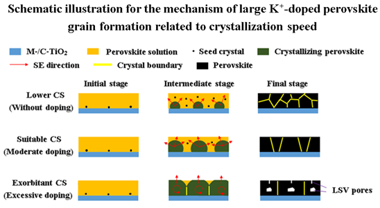
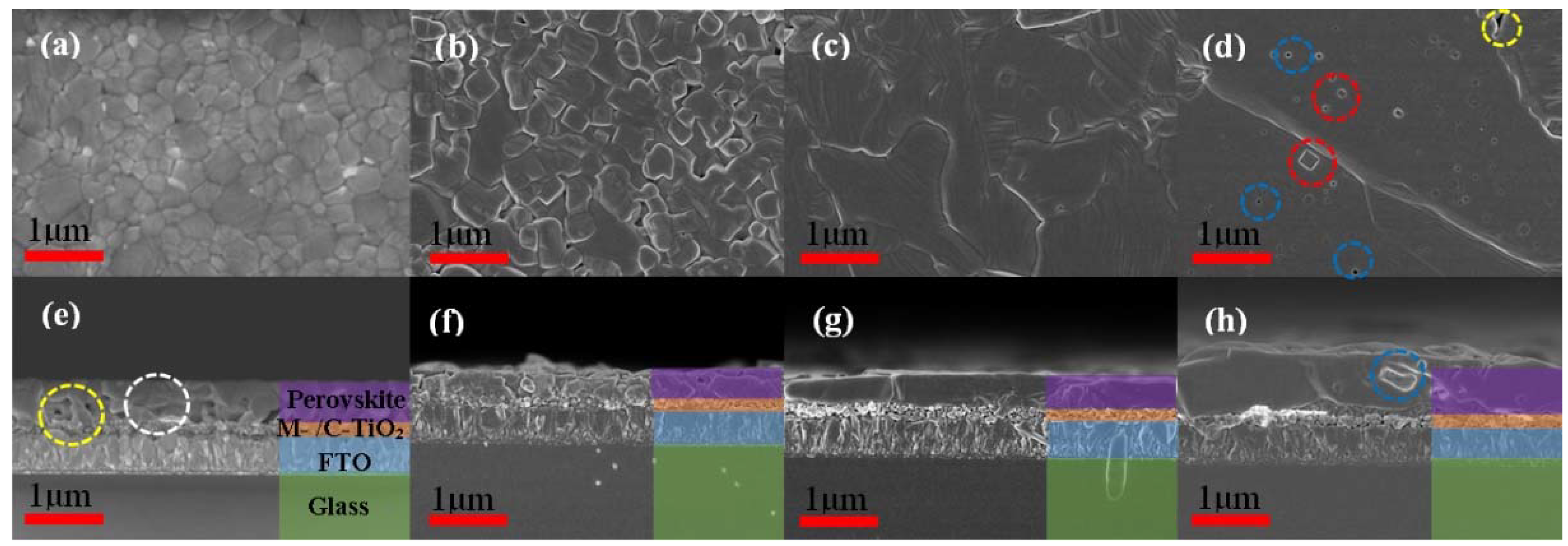
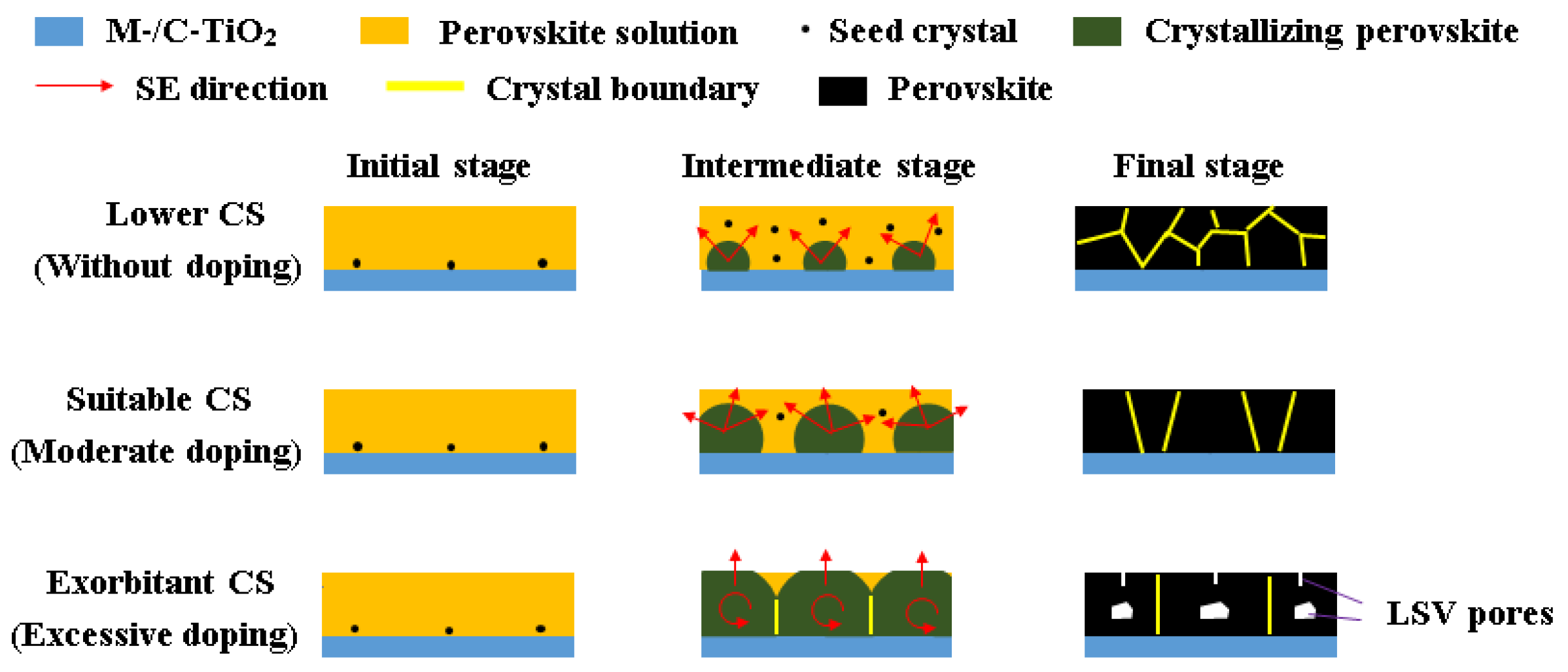
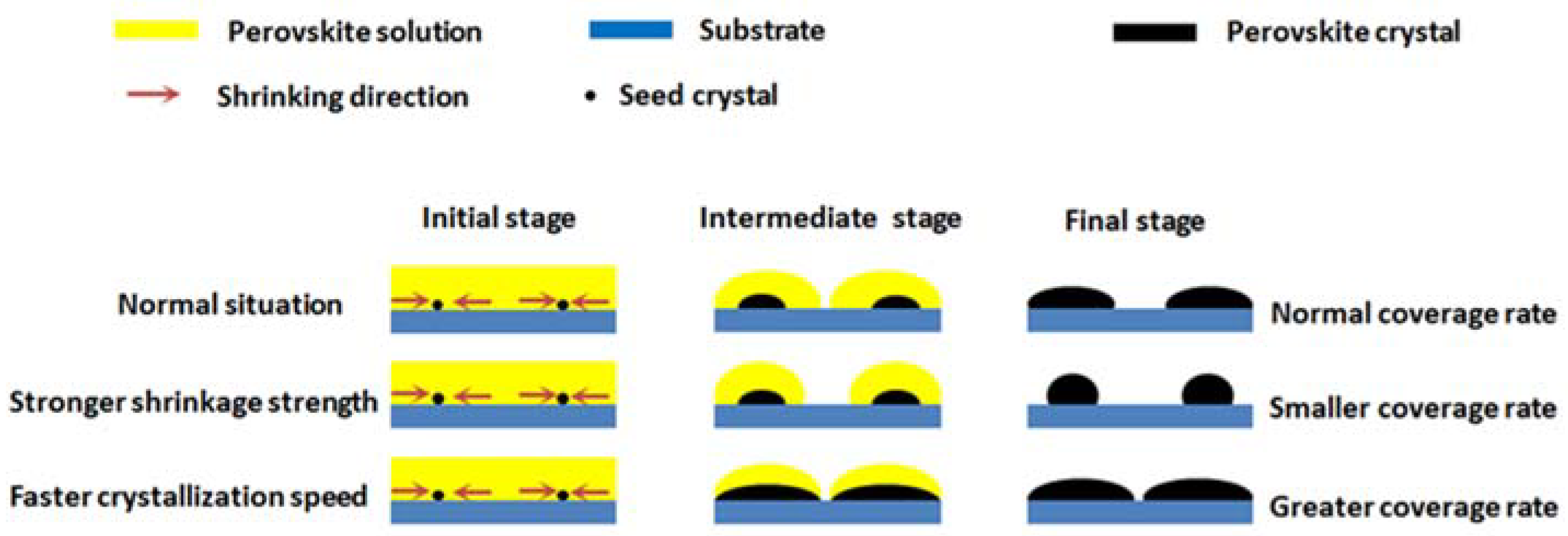
3. Results and Discussion
4. Conclusions
Author Contributions
Funding
Conflicts of Interest
References
- Park, N.-G. Organometal perovskite light absorbers toward a 20% efficiency low-cost solid-state mesoscopic solar cell. J. Phys. Chem. Lett. 2013, 4, 2423–2429. [Google Scholar] [CrossRef]
- Yang, W.S.; Noh, J.H.; Jeon, J.N.; Kim, Y.C.; Ryu, S.C.; Seo, S.J.; Seok, S.I.I. High-performance photovoltaic perovskite layers fabricated through intramolecular exchange. Science 2015, 348, 1234–1237. [Google Scholar] [CrossRef] [PubMed]
- Saliba, M.; Matsui, T.; Domanski, K.; Seo, J.-Y.; Ummadisingu, A.; Zakeeruddin, S.M.; Correa-Baena, J.-P.; Tress, W.R.; Abate, A.; Hagfeldt, A.; et al. Incorporation of rubidium cations into perovskite solar cells improves photovoltaic performance. Science 2016, 354, 206–209. [Google Scholar] [CrossRef] [PubMed]
- Shin, S.S.; Yeom, E.J.; Yang, W.S.; Hur, S.; Kim, M.G.; Im, J.; Seo, J. Colloidally prepared La-doped BaSnO3 electrodes for efficient, photostable perovskite solar cells. Science 2017, 356, 167–171. [Google Scholar] [CrossRef] [PubMed]
- Tang, Z.G.; Uchida, S.; Bessho, T.; Kinoshita, T.; Wang, H.B.; Awai, F.; Jono, R.; Maitani, M.M.; Nakazaki, J.; Kubo, T.; et al. Modulations of various alkali metal cations on organometal halide perovskites and their influence on photovoltaic performance. Nano Energy 2018, 45, 184–192. [Google Scholar] [CrossRef]
- Stranks, S.D.; Eperon, G.E.; Grancini, G.; Menelaou, C.; Alcocer, M.J.P.; Leijtens, T.; Herz, L.M.; Petrozza, A.; Snaith, H.J. Electron-Solvent-vapor-pore Diffusion Lengths Exceeding 1 Micrometer in an Organometal Trihalide Perovskite Absorber. Science 2013, 342, 341–344. [Google Scholar] [CrossRef] [PubMed]
- Eperon, G.E.; Burlakov, V.M.; Docampo, P.; Goriely, A.; Snaith, H.J. Morphological Control for High Performance, Solution-Processed Planar Heterojunction Perovskite Solar Cells. Adv. Funct. Mater. 2014, 24, 151–157. [Google Scholar] [CrossRef]
- Chen, Z.; Li, H.; Tang, Y.; Huang, X.; Ho, D.; Lee, C.-S. Shape-Controlled Synthesis of Organolead Halide Perovskite Nanocrystals and Their Tunable Optical Absorption. Mater. Res. Express 2014, 1, 015034. [Google Scholar] [CrossRef]
- Yin, W.J.; Shi, T.; Yan, Y. Unique Properties of Halide Perovskites as Possible Origins of the Superior Solar Cell Performance. Adv. Mater. 2014, 26, 4653–4658. [Google Scholar] [CrossRef] [PubMed]
- Brenner, T.M.; Egger, D.A.; Kronik, L.; Hodes, G.; Cahen, D. Hybrid organic–inorganic perovskites: Low-cost semiconductors with intriguing charge-transport properties. Nat. Rev. Mater. 2016, 1, 15007. [Google Scholar] [CrossRef]
- Bai, X.; Zou, X.; Zhu, J.; Pei, Y.; Yang, Y.; Jin, W.; Chen, D. Effect of Rb doping on modulating grain shape and semiconductor properties of MAPbI3 perovskite layer. Mater. Lett. 2018, 211, 328–330. [Google Scholar] [CrossRef]
- Yang, Y.; Zou, X.; Pei, Y.; Bai, X.; Jin, W.; Chen, D. Effect of doping of NaI monovalent cation halide on the structural, morphological, optical and optoelectronic properties of MAPbI3 perovskite. J. Mater. Sci. Mater. Electron. 2018, 29, 205–210. [Google Scholar] [CrossRef]
- Zhu, F.; Zhang, P.; Wu, X.; Fu, L.; Zhang, J.; Xu, D. The origin of higher open-circuit voltage in Zn-doped TiO2 nanoparticle-based dye-sensitized solar cells. ChemPhysChem 2012, 13, 3731. [Google Scholar] [CrossRef] [PubMed]
- Gao, Y.; Yip, H.L.; Chen, K.S.; O’malley, K.M.; Acton, O.; Sun, Y.; Ting, G.; Chen, H.; Jen, A.K.Y. Surface Doping of Conjugated Polymers by Graphene Oxide and Its Application for Organic Electronic Devices. Adv. Mater. 2011, 23, 1903. [Google Scholar] [CrossRef] [PubMed]
- Li, Z.; Yang, M.; Park, J.S.; Wei, S.H.; Berry, J.J.; Zhu, K. Stabilizing Perovskite Structures by Tuning Tolerance Factor: Formation of Formamidinium and Cesium Lead Iodide Solid-State Alloys. Chem. Mater. 2016, 28, 284–292. [Google Scholar] [CrossRef]
- Saliba, M.; Matsui, T.; Seo, J.-Y.; Domanski, K.; Correa-Baena, J.-P.; Nazeeruddin, M.K.; Zakeeruddin, S.M.; Tress, W.; Abate, A.; Hagfeldt, A.; et al. Cesium-containing triple cation perovskite solar cells: Improved stability, reproducibility and high efficiency. Energy Environ. Sci. 2016, 9, 1989–1997. [Google Scholar] [CrossRef] [PubMed]
- Syzgantseva, O.A.; Saliba, M.; Grätzel, M.; Rothlisberger, U. Stabilization of the Perovskite Phase of Formamidinium Lead Triiodide by Methylammonium, Cs, and/or Rb Doping. J. Phys. Chem. Lett. 2017, 8, 1191–1196. [Google Scholar] [CrossRef] [PubMed]
- Nam, J.K.; Chai, S.U.; Cha, W.; Choi, Y.J.; Kim, W.; Jung, M.S.; Kwon, J.; Kim, D.; Park, J.H. Potassium Incorporation for Enhanced Performance and Stability of Fully Inorganic Cesium Lead Halide Perovskite Solar Cells. Nano Lett. 2017, 17, 2028–2033. [Google Scholar] [CrossRef] [PubMed]
- Chang, J.; Lin, Z.; Zhu, H.; Isikgor, F.H.; Xu, Q.-H.; Zhang, C.; Hao, Y.; Ouyang, J. Enhancing the photovoltaic performance of planar heterojunction perovskite solar cells by doping the perovskite layer with alkali metal ions. J. Mater. Chem. A 2016, 4, 16546–16552. [Google Scholar] [CrossRef]
- Zhao, P.; Yin, W.; Kim, M.; Han, M.; Song, J. Improved carriers injection capacity in perovskite solar cells by introducing A-site interstitial defects. J. Mater. Chem. A 2017, 5, 7905–7911. [Google Scholar] [CrossRef]
- Bag, S.; Durstock, M.F. Large Perovskite Grain Growth in Low-Temperature Solution-Processed Planar p-i-n Solar Cells by Sodium Addition. ACS Appl. Mater. Interfaces 2016, 8, 5053–5057. [Google Scholar] [CrossRef] [PubMed]
- Bi, C.; Zheng, X.; Chen, B.; Wei, H.; Huang, J. Spontaneous Passivation of Hybrid Perovskite by Sodium Ions from Glass Substrates: Mysterious Enhancement of Device Efficiency Revealed. ACS Energy Lett. 2017, 2, 1400–1406. [Google Scholar] [CrossRef]
- Tang, Z.G.; Bessho, T.; Awai, F.; Kinoshita, T.; Maitani, M.M.; Jono, R.; Murakami, T.N.; Wang, H.B.; Kubo, T.; Uchida, S.; et al. Hysteresis-free perovskite solar cells made of potassium-doped organometal halide perovskite. Sci. Rep. 2017, 7, 12183. [Google Scholar] [CrossRef] [PubMed] [Green Version]
- Yao, D.S.; Zhang, C.M.; Pham, N.D.; Zhang, Y.H.; Tiong, V.T.; Du, A.J.; Shen, Q.; Wilson, G.J.; Wang, H.X. Hindered Formation of Photo-Inactive δ-FAPbI3 Phase and Hysteresis-Free Mixed-Cation Planar Heterojunction Perovskite Solar Cells with Enhanced Efficiency via Potassium Incorporation. J. Phys. Chem. Lett. 2018, 9, 2113–2120. [Google Scholar] [CrossRef] [PubMed]
- Kubicki, D.J.; Prochowicz, D.; Hofstetter, A.; Zakeeruddin, S.M.; Gratzel, M.; Emsley, L. Phase Segregation in Potassium-Doped Lead Halide Perovskites from K-39 Solid-State NMR at 21.1 T. J. Am. Chem. Soc. 2018, 140, 7232–7238. [Google Scholar] [CrossRef] [PubMed]
- Abdi-Jalebi, M.; Andaji-Garmaroudi, Z.; Cacovich, S.; Stavrakas, C.; Philippe, B.; Richter, J.M.; Alsari, M.; Booker, E.P.; Hutter, E.M.; Pearson, A.J.; et al. Maximizing and stabilizing luminescence from halide perovskites with potassium passivation. Nature 2018, 555, 497–501. [Google Scholar] [CrossRef] [PubMed]
- Kubicki, D.J.; Prochowicz, D.; Hofstetter, A.; Zakeeruddin, S.M.; Gratzel, M.; Emsley, L. Phase Segregation in Cs-, Rb- and K-Doped Mixed-Cation (MA)x(FA)1−xPbI3 Hybrid Perovskites from Solid-State NMR. J. Am. Chem. Soc. 2017, 139, 14173–14180. [Google Scholar] [CrossRef] [PubMed]
- Kojima, A.; Teshima, K.; Shirai, Y.; Miyasaka, T. Organometal halide perovskites as visible-light sensitizers for photovoltaic cells. J. Am. Chem. Soc. 2009, 131, 6050–6051. [Google Scholar] [CrossRef] [PubMed]
- Yang, W.S.; Park, B.-W.; Jung, E.H.; Jeon, N.J.; Kim, Y.C.; Lee, D.U.; Shin, S.S.; Seo, J.; Kim, E.K.; Noh, J.H.; et al. Iodide management in formamidinium-lead-halide-based perovskite layers for efficient solar cells. Science 2017, 356, 1376–1379. [Google Scholar] [CrossRef] [PubMed]
- Mei, A.; Li, X.; Liu, L.; Ku, Z.; Liu, T.; Rong, Y.G.; Xu, M.; Hu, M.; Chen, J.; Yang, Y.; et al. A hole-conductor-free, fully printable mesoscopic perovskite solar cell with high stability. Science 2014, 345, 295–298. [Google Scholar] [CrossRef] [PubMed]
- Habisreutinger, S.N.; Leijtens, T.; Eperon, G.E.; Stranks, S.D.; Nicholas, R.J.; Snaith, H.J. Carbon nanotube/polymer composites as a highly stable hole collection layer in perovskite solar cells. Nano Lett. 2014, 14, 5561–5568. [Google Scholar] [CrossRef] [PubMed]
- Wei, Z.; Yan, K.; Chen, H.; Yi, Y.; Zhang, T.; Long, X.; Li, J.; Zhang, L.; Wang, J.; Yang, S. Cost-efficient clamping solar cells using candle soot for hole extraction from ambipolar perovskites. Energy Environ. Sci. 2014, 7, 3326–3333. [Google Scholar] [CrossRef]
- Zhang, N.; Guo, Y.; Yin, X.; He, M.; Zou, X. Spongy carbon film deposited on a separated substrate as counter electrode for perovskite-based solar cell. Mater. Lett. 2016, 182, 248–252. [Google Scholar] [CrossRef]
- Ling, T.; Zou, X.; Cheng, J.; Bai, X.; Ren, H.; Chen, D. Modified Sequential Deposition Route through Localized-Liquid-Liquid-Diffusion for Improved Perovskite Multi-Crystalline Thin Films with Micrometer-Scaled Grains for Solar Cells. Nanomaterials 2018, 8, 416. [Google Scholar] [CrossRef] [PubMed]
- Uz Zaman, M.M.; Imran, M.; Saleem, A.; Kamboh, A.H.; Arshad, M.; Khan, N.A.; Akhter, P. Potassium doped methylammonium lead iodide (MAPbI3) thin films as a potential absorber for perovskite solar cells; structural, morphological, electronic and optoelectric properties. Phys. B Condens. Matter 2017, 522, 57–65. [Google Scholar] [CrossRef]
- Luo, D.; Yu, L.; Wang, H.; Zou, T.; Luo, L.; Liu, Z.; Lu, Z. Cubic structure of the mixed halide perovskite CH3NH3PbI3−xClx via thermal annealing. RSC Adv. 2015, 5, 85480–85485. [Google Scholar] [CrossRef]
- Li, C.; Guerrero, A.; Zhong, Y.; Graser, A.; Luna, C.A.M.; Kohler, J.; Bisquert, J.; Hildner, R.; Huettner, S. Real-Time Observation of Iodide Ion Migration in Methylammonium Lead Halide Perovskites. Small 2017, 13, 1701711. [Google Scholar] [CrossRef] [PubMed] [Green Version]
- Sun, Q.; Gong, X.; Li, H.; Liu, S.; Zhao, X.; Shen, Y.; Wang, M. Direct formation of I3− ions in organic cation solution for efficient perovskite solar cells. Sol. Energy Mater. Sol. Cells 2018, 185, 111–116. [Google Scholar] [CrossRef]


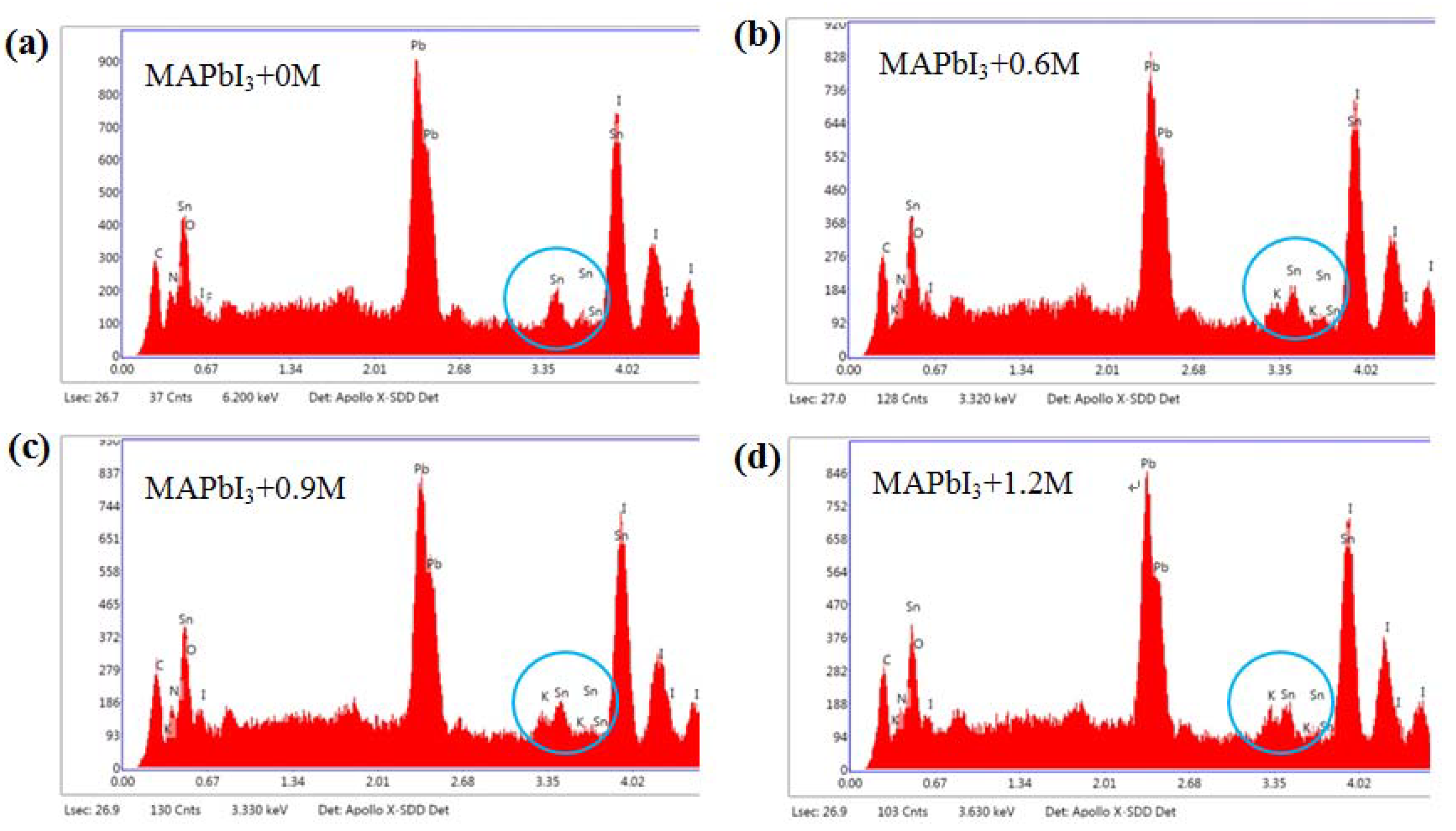
| Sample | K K | C K | N K | O K | Pb M | Sn L | I L |
|---|---|---|---|---|---|---|---|
| MAPbI3+0M | 0 | 5.10 | 2.35 | 0.80 | 23.49 | 5.84 | 62.42 |
| MAPbI3+0.6M | 1.44 | 4.58 | 2.18 | 0.49 | 21.77 | 5.40 | 64.14 |
| MAPbI3+0.9M | 1.50 | 4.59 | 1.73 | 0.38 | 22.21 | 5.67 | 63.92 |
| MAPbI3+1.2M | 1.80 | 4.50 | 2.07 | 0.55 | 21.71 | 5.26 | 64.11 |
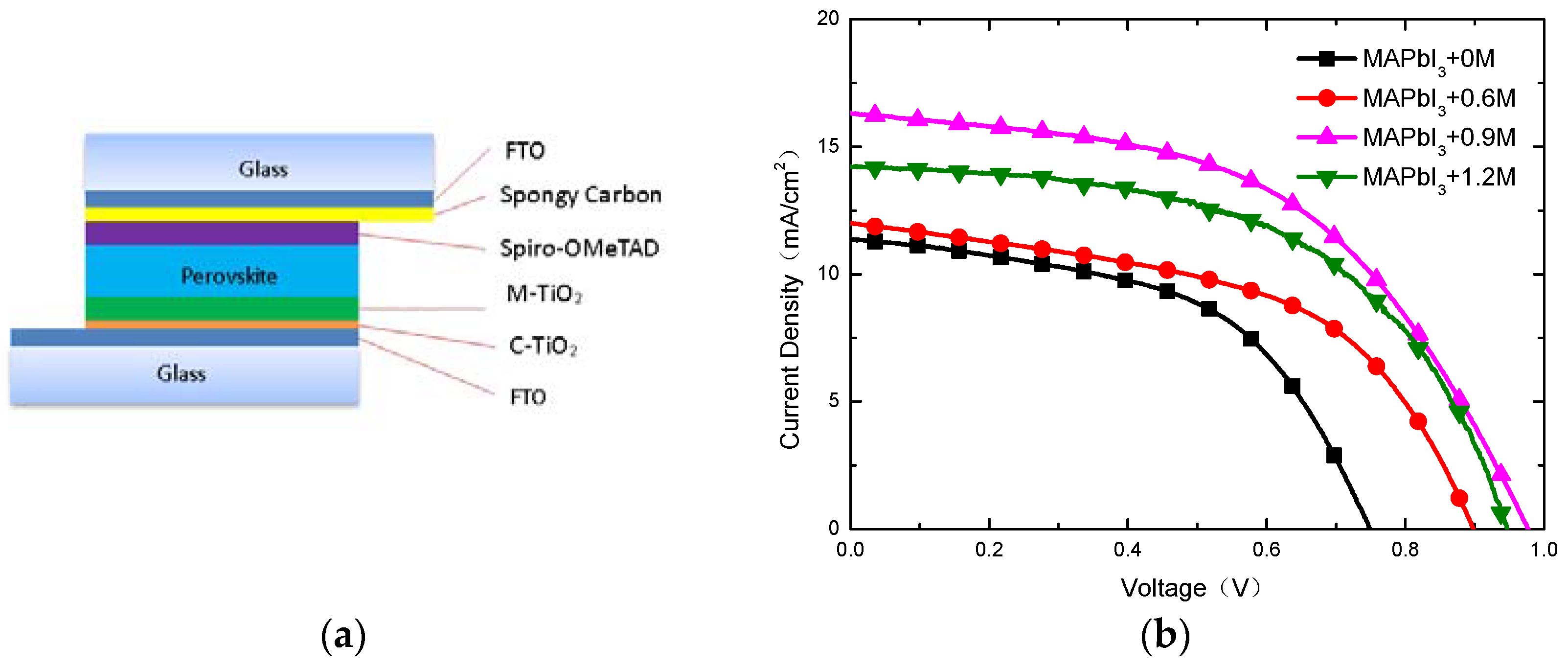
| DC a | Jsc b (mA/cm−2) | Voc c (v) | FF d | PCE (%) |
|---|---|---|---|---|
| 0 M | 11.37 | 0.75 | 0.52 | 4.43 |
| 0.6 M | 12.01 | 0.90 | 0.52 | 5.62 |
| 0.9 M | 16.33 | 0.98 | 0.51 | 8.14 |
| 1.2 M | 14.20 | 0.95 | 0.55 | 7.42 |
© 2018 by the authors. Licensee MDPI, Basel, Switzerland. This article is an open access article distributed under the terms and conditions of the Creative Commons Attribution (CC BY) license (http://creativecommons.org/licenses/by/4.0/).
Share and Cite
Ling, T.; Zou, X.; Cheng, J.; Yang, Y.; Ren, H.; Chen, D. Modulating Surface Morphology Related to Crystallization Speed of Perovskite Grain and Semiconductor Properties of Optical Absorber Layer under Controlled Doping of Potassium Ions for Solar Cells. Materials 2018, 11, 1605. https://doi.org/10.3390/ma11091605
Ling T, Zou X, Cheng J, Yang Y, Ren H, Chen D. Modulating Surface Morphology Related to Crystallization Speed of Perovskite Grain and Semiconductor Properties of Optical Absorber Layer under Controlled Doping of Potassium Ions for Solar Cells. Materials. 2018; 11(9):1605. https://doi.org/10.3390/ma11091605
Chicago/Turabian StyleLing, Tao, Xiaoping Zou, Jin Cheng, Ying Yang, Haiyan Ren, and Dan Chen. 2018. "Modulating Surface Morphology Related to Crystallization Speed of Perovskite Grain and Semiconductor Properties of Optical Absorber Layer under Controlled Doping of Potassium Ions for Solar Cells" Materials 11, no. 9: 1605. https://doi.org/10.3390/ma11091605