Trap-Assisted Charge Injection into Large Bandgap Polymer Semiconductors


 , and
, and 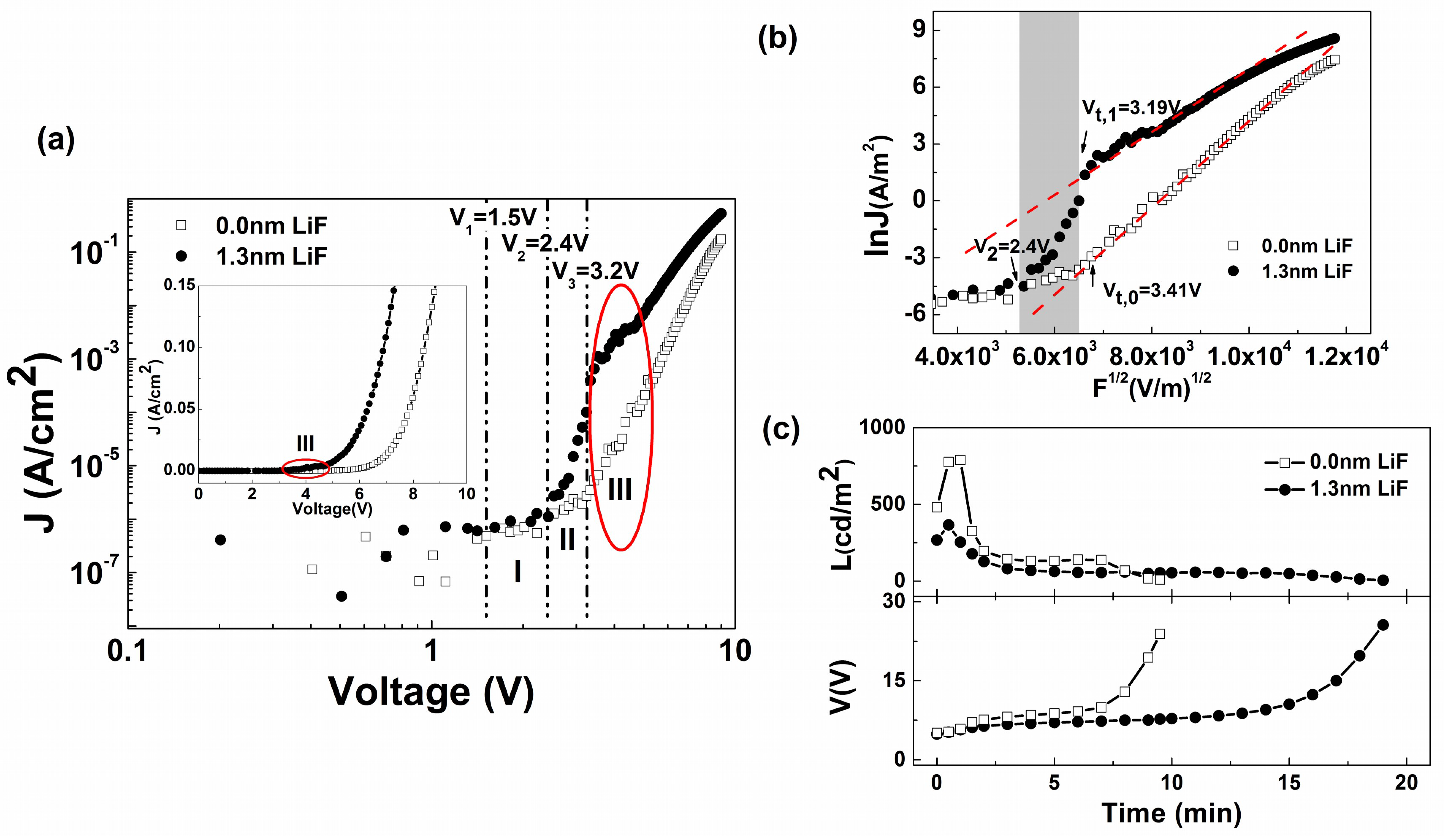
Abstract
:1. Introduction
2. Materials and Methods
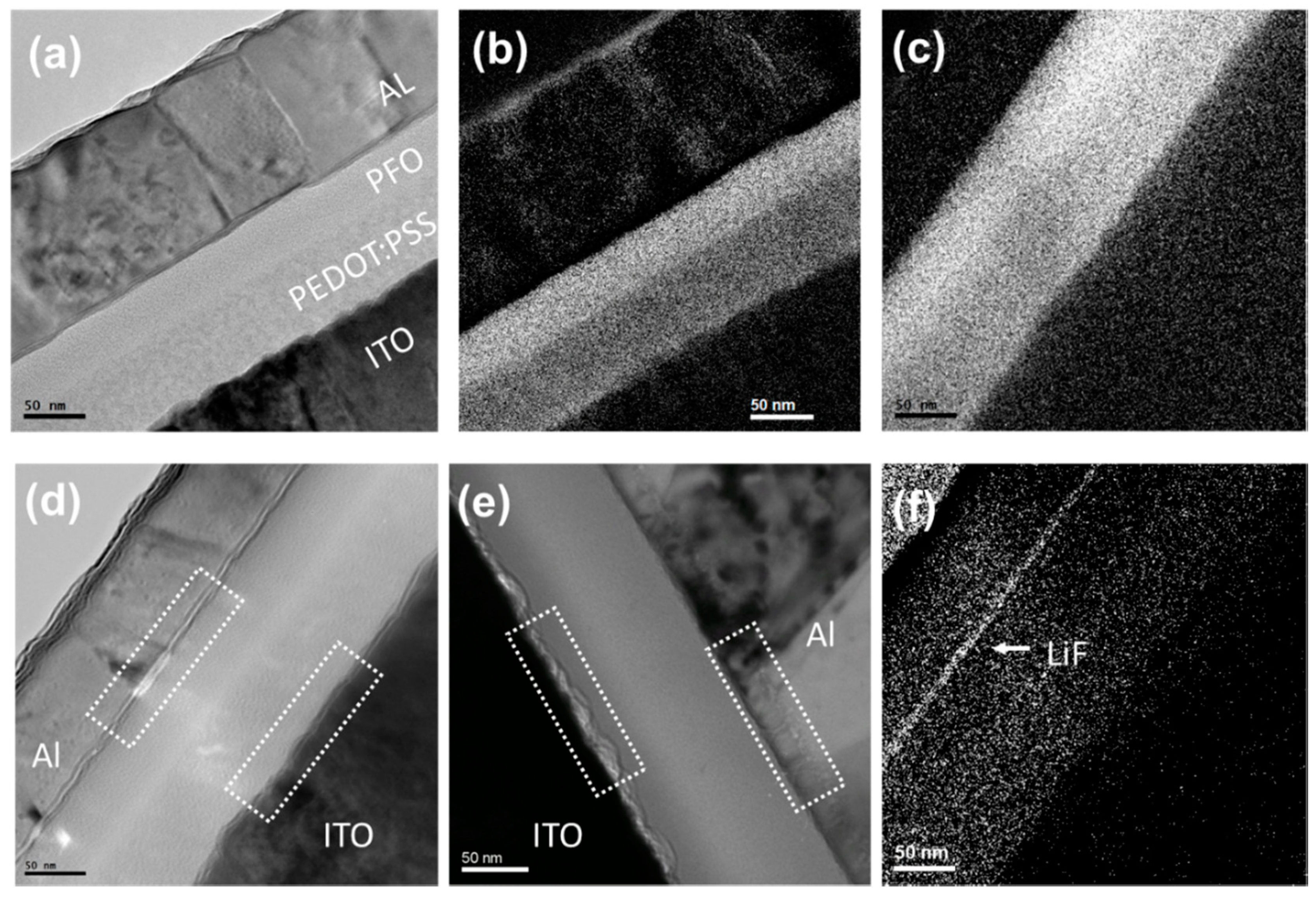
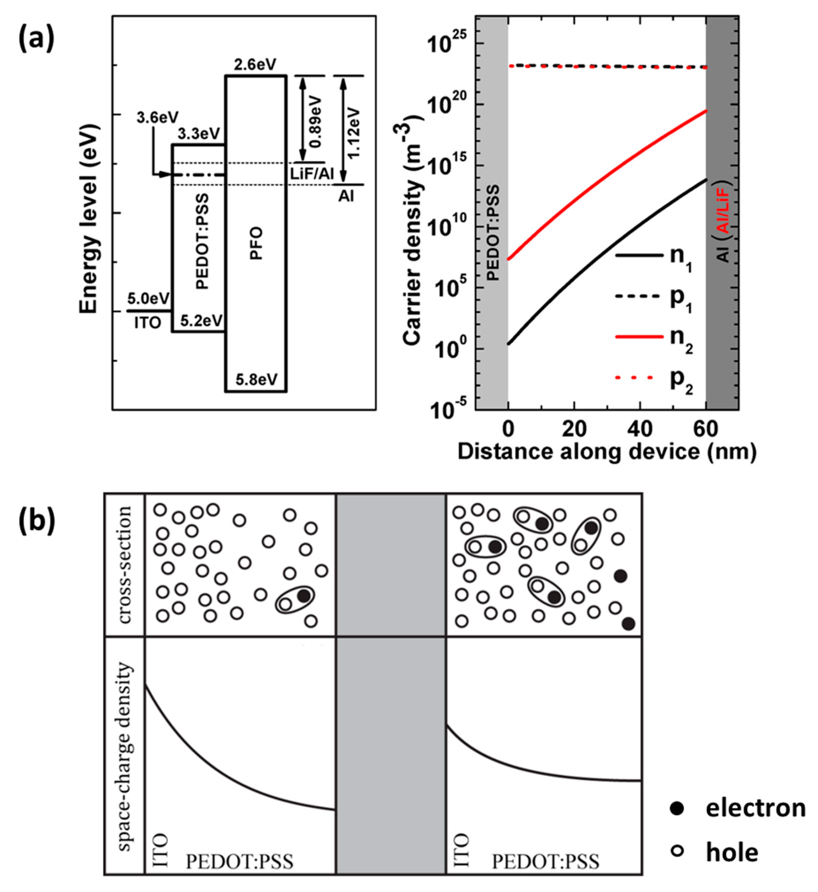
3. Results and Discussion
4. Conclusions
Supplementary Materials
Author Contributions
Funding
Conflicts of Interest
References
- Burroughes, J.H.; Bradley, D.D.C.; Brown, A.R.; Marks, R.N.; Mackay, K.; Friend, R.H.; Burns, P.L.; Holmes, A.B. Light-emitting diodes based on conjugated polymers. Nature 1990, 347, 539–541. [Google Scholar] [CrossRef]
- So, F.; Kondakov, D. Degradation mechanisms in small-molecule and polymer organic light-emitting diodes. Adv. Mater. 2010, 22, 3762–3777. [Google Scholar] [CrossRef] [PubMed]
- Neher, D. Polyfluorene Homopolymers: Conjugated Liquid-Crystalline Polymers for Bright Blue Emission and Polarized Electroluminescence. Macromol. Rapid Commun. 2001, 22, 1365–1385. [Google Scholar] [CrossRef]
- Woudenbergh, T.V.; Wildeman, J.; Blom, P.W.M.; Bastiaansen, J.J.A.M.; Langeveld-Voss, B.M.W. Electron-enhanced hole injection in blue polyfluorene-based polymer light-emitting diodes. Adv. Funct. Mater. 2004, 7, 677–683. [Google Scholar] [CrossRef]
- Lane, P.A.; deMello, J.C.; Fletcher, R.B.; Bernius, M. Electric filed screening in polymer light-emitting diodes. App. Phys. Lett. 2003, 83, 3611–3613. [Google Scholar] [CrossRef]
- Brewer, P.J.; Lane, P.A.; deMello, A.J.; Bradley, D.D.C.; deMello, J.C. Internal field screening in polymer light-emitting diodes. Adv. Funct. Mater. 2004, 14, 562–570. [Google Scholar] [CrossRef]
- Brewer, P.J.; Lane, P.A.; Huang, J.; deMello, A.J.; Bradley, D.D.C.; deMello, J.C. Role of electron injection in polyfluorene-based light emitting diodes containing PEDOT:PSS. Phys. Rev. B 2005, 71, 205209. [Google Scholar] [CrossRef]
- Brewer, P.J.; Huang, J.; Lane, P.A.; deMello, A.J.; Bradley, D.D.C.; deMello, J.C. Influence of poly(3,4-ethylenedioxythiophene)-poly(styrenesulfonate) in polymer LEDs. Phys. Rev. B 2006, 74, 115202. [Google Scholar] [CrossRef]
- Poplavskyy, D.; Nelson, J.; Bradley, D.D.C. Ohmic hole injection in poly(9,9-dioctylfluorene) polymer light-emitting diodes. App. Phys. Lett. 2003, 83, 707–709. [Google Scholar] [CrossRef]
- Murata, K.; Cinà, S.; Greenham, N.C. Barriers to electron extraction in polymer light-emitting diodes. Appl. Phys. Lett. 2001, 79, 1193–1195. [Google Scholar] [CrossRef]
- Kanaan, H.; Jolinat, P.; Ablart, G.; Destruel, P.; Renaud, C.; Lee, C.W.; Nguyen, T.P. Influence of poly(3,4-ethylenedioxythiophene)-poly(styrenesulfonate) in polyfluorene-based light-emitting diodes: Evidence of charge trapping at the organic interface. Org. Electron. 2010, 11, 1047–1052. [Google Scholar] [CrossRef]
- Nguyen, T.P.; Renaud, C. Interface effects on the defect state formation in organic devices. In Organic Photonic Materials and Devices XI, Proceedings of SPIE XI, San Jose, CA, USA, 27–29 January 2009; International Society for Optics and Photonics: Bellingham, WA, USA, 2009; Volume 7213, p. 721314. [Google Scholar]
- Bange, S.; Kuksov, A.; Neher, D.; Vollmer, A.; Koch, N.; Ludemann, A.; Heun, S. The role of poly(3,4-ethylenedioxythiophene):poly(styrenesulphonate) as a hole injection layer in a blue-emitting polymer light-emitting diode. J. Appl. Phys. 2008, 104, 104506. [Google Scholar] [CrossRef]
- Welz, S.; Browning, N.; Minor, A.M. Shadow FIBing—Using geometry to prepare TEM samples. Microsc. Michoanal. 2005, 11 (Suppl. 2), 834–835. [Google Scholar] [CrossRef]
- Kim, S.; Liu, G.; Minor, A.M. FIB sample preparation of polymer thin films on hard substrates using the shadow-FIB method. Microsc. Today 2009, 17, 20–23. [Google Scholar] [CrossRef]
- Kim, S.; Park, M.J.; Balsara, N.P.; Liu, G.; Minor, A.M. Minimization of focused ion beam damage in nanostructured polymer thin films. Ultramicroscopy 2011, 111, 191–199. [Google Scholar] [CrossRef] [PubMed]
- Davids, P.S.; Campbell, I.H.; Smith, D.L. Device model for single carrier organic diodes. J. Appl. Phys. 1997, 82, 6319–6325. [Google Scholar] [CrossRef]
- Scott, J.C.; Malliaras, G.G. Charge injection and recombination at the metal–organic interface. Chem. Phys. Lett. 1999, 299, 115–119. [Google Scholar] [CrossRef]
- Kondakov, D.Y.; Sandifer, J.R.; Tang, C.W.; Young, R.H. Nonradiative recombination centers and electrical aging of organic light emitting diodes: Direct connection between accumulation of trapped charge and luminance loss. J. Appl. Phys. 2003, 93, 1108–1119. [Google Scholar] [CrossRef]
- Bodrozic, V.; Brown, T.M.; Mian, S.; Caruana, D.; Roberts, M.; Phillips, N.; Halls, J.J.; Grizzi, I.; Burroughes, J.H.; Cacialli, F. The built-in potential in blue polyfluorene-based light-emitting diodes. Adv. Mater. 2008, 20, 2410–2415. [Google Scholar] [CrossRef]
- De Vries, R.J.; Van Mensfoort, S.L.M.; Janssen, R.A.J.; Coehoorn, R. Relation between the built-in voltage in organic light-emitting diodes and the zero-field voltage as measured by electroabsorption. Phys. Rev. B 2010, 81, 125203. [Google Scholar] [CrossRef] [Green Version]
- Parker, I.D. Carrier tunneling and device characteristics in polymer lightemitting diodes. J. Appl. Phys. 1994, 75, 1656–1666. [Google Scholar] [CrossRef]
- Parker, I.D.; Cao, Y.; Yang, C.Y. Lifetime and degradation effects in polymer light-emitting diodes. J. Appl. Phys. 1999, 85, 2441–2447. [Google Scholar] [CrossRef]
- Barth, S.; Wolf, U.; Bässler, H.; Müller, P.; Riel, H.; Vestweber, H.; Seidler, P.F.; Rieß, W. Current injection from a metal to a disordered hopping system. III. Comparison between experiment and Monte Carlo simulation. Phys. Rev. B 1999, 60, 8791–8797. [Google Scholar] [CrossRef]
- Arkhipov, V.; Bässler, H. Tandem injection of charge carriers across a metal-dielectric interface. App. Phys. Lett. 2000, 77, 2758–2760. [Google Scholar] [CrossRef]
- Van Duren, J.K.J.; Loos, J.; Morrissey, F.; Leewis, C.M.; Kivits, K.P.H.; van IJzendoorn, L.J.; Rispens, M.T.; Hummelen, J.C.; Janssen, R.A.J. In-Situ compositional and structural analysis of plastic solar cells. Adv. Funct. Mater. 2002, 12, 665–669. [Google Scholar] [CrossRef]
- Steuerman, D.W.; Garcia, A.; Dante, M.; Yang, R.; Löfvander, J.P.; Nguyen, T.Q. Imaging the interfaces of conjugated polymer optoelectronic devices. Adv. Mater. 2008, 20, 528–534. [Google Scholar] [CrossRef]
- Aziz, H.; Popovic, Z.D.; Hu, N.X.; Hor, A.M.; Xu, G. Degradation mechanism of small molecule-based organic light-emitting devices. Science 1999, 283, 1900–1902. [Google Scholar] [CrossRef] [PubMed]
- Tse, S.C.; Tsang, S.W.; So, S.K. Polymeric conducting anode for small organic transporting molecules in dark injection experiments. J. Appl. Phys. 2006, 100, 063708. [Google Scholar] [CrossRef]
- Kao, K.C.; Hwang, W. Electrical Transport in Solids: With Particular Reference to Organic Semiconductors; Pergamon Press: Oxford, UK, 1981. [Google Scholar]
- Carter, S.A.; Angelopoulos, M.; Karg, S.; Brock, P.J.; Scott, J.C. Polymeric anodes for improved polymer light-emitting diode performance. App. Phys. Lett. 1997, 70, 2067–2069. [Google Scholar] [CrossRef] [Green Version]
- Hung, L.S.; Tang, C.W.; Mason, M.G. Enhanced electron injection in organic electroluminescence devices. App. Phys. Lett. 1997, 70, 152–154. [Google Scholar] [CrossRef]
- De Kok, M.M.; Buechel, M.; Vulto, S.I.E.; de Weijer, P.; Meulenkamp, E.A.; de Winter, S.H.P.M.; Mank, A.J.G.; Vorstenbosch, H.J.M.; Weijtens, C.H.L.; van Elsbergen, V. Modification of PEDOT:PSS as hole injection layer in polymer LEDs. Phys. Status Sol. A 2004, 201, 1342–1359. [Google Scholar] [CrossRef]
- Brown, T.M.; Millard, I.S.; Lacey, D.J.; Burroughes, J.H.; Friend, R.H.; Cacialli, F. The influence of LiF thickness on the built-in potential of blue polymer light-emitting diodes with LiF/Al cathodes. Synth. Met. 2001, 124, 15–17. [Google Scholar] [CrossRef]
- Sohn, S.; Park, K.; Lee, D.; Jung, D.; Kim, H.M.; Manna, U.; Yi, J.; Boo, J.; Chae, H.; Kim, H. Characteristics of polymer light emitting diodes with the LiF anode interfacial layer. Jpn. J. Appl. Phys. 2006, 45, 3733–3736. [Google Scholar] [CrossRef]
- Van Woudenbergh, T.; Blom, P.W.M.; Huiberts, J.N. Electro-optical properties of a polymer light-emitting diode with an injection-limited hole contact. App. Phys. Lett. 2003, 82, 985–987. [Google Scholar] [CrossRef] [Green Version]
- Lu, M.; de Bruyn, P.; Nicolai, H.T.; Wetzelaer, G.A.H.; Blom, P.W.M. Hole-enhanced electron injection from ZnO in inverted polymer light-emitting diodes. Org. Electron. 2012, 13, 1693–1699. [Google Scholar] [CrossRef] [Green Version]

© 2019 by the authors. Licensee MDPI, Basel, Switzerland. This article is an open access article distributed under the terms and conditions of the Creative Commons Attribution (CC BY) license (http://creativecommons.org/licenses/by/4.0/).
Share and Cite
Wang, D.; Fina, M.; Kim, S.; Zhang, C.; Zhang, T.; Deng, Y.; Chen, K.; Liang, L.; Mao, S.S.; Minor, A.M.; et al. Trap-Assisted Charge Injection into Large Bandgap Polymer Semiconductors. Materials 2019, 12, 2427. https://doi.org/10.3390/ma12152427
Wang D, Fina M, Kim S, Zhang C, Zhang T, Deng Y, Chen K, Liang L, Mao SS, Minor AM, et al. Trap-Assisted Charge Injection into Large Bandgap Polymer Semiconductors. Materials. 2019; 12(15):2427. https://doi.org/10.3390/ma12152427
Chicago/Turabian StyleWang, Dongdong, Michael Fina, Suhan Kim, Chunmei Zhang, Ting Zhang, Yonghong Deng, Kai Chen, Lijuan Liang, Samuel S. Mao, Andrew M. Minor, and et al. 2019. "Trap-Assisted Charge Injection into Large Bandgap Polymer Semiconductors" Materials 12, no. 15: 2427. https://doi.org/10.3390/ma12152427