1. Introduction
Organic thin-film transistors (OTFTs) have been attracting interest owing to their developing applications in low-cost, light-weight, and flexible electronic devices such as active-matrix displays [
1], radio frequency identification tags [
2], and bio and chemical sensors [
3]. Over the years, progress in semiconducting materials and fabrication techniques has dramatically increased the charge mobility in these devices to well above 1 cm
2 V
−1 s
−1 [
4,
5]. However, in general, these devices operate with relatively high gate voltages (V
G ≥ 3 V) which hinders their integration in low-voltage, portable applications [
6]. In order to enable organic TFTs that operate below 3 V and deliver high output current, the use of ultra-thin, high dielectric constant (high-κ) materials such as HfO
2, Ta
2O
5, TiO
2, ZrO
2, Al
2O
3, Y
2O
3, CeO
2 [
7,
8,
9] is required. In particular, tantalum pentoxide (Ta
2O
5) is a very promising candidate due to the high dielectric constant in the bulk (κ
bulk ~27) and as a thin-film (κ
thin-film ~20). These values are at least two times larger than that of Al
2O
3 (κ
bulk ~9) [
10] and five times larger than that of SiO
2 (κ
bulk ~3.9). As a result, Ta
2O
5 has been abundantly used in electrolytic capacitors, DRAM devices, and recently in solution-processed inorganic semiconductor thin-film transistors as a promising gate dielectric for low-power electronics [
11].
A common way to deposit a high-quality, pinhole-free film of tantalum oxide is by atomic layer deposition (ALD). However, ALD is a relatively slow process and requires a high vacuum which is not suitable for low-cost, large-area deposition [
12]. Alternatively, magnetron sputtering deposition (MSD) has been used to form tantalum oxide films [
13]. However, it is a time-consuming, high vacuum technique which suffers from the same drawbacks as ALD. Recently, anodic oxidation (so-called anodization) has attracted a lot of attention because it is a low-cost, solution-based deposition process that can be performed under ambient conditions [
14]. Anodization is a self-limiting and self-healing process that gives pinhole-free, homogenous oxide layers that can be grown in an ambient atmosphere at room temperature. Previously, low voltage poly(3-hexylthiophene-2,5-diyl) (P3HT) TFTs operating at 3 V using thick (d > 100 nm), e-beam deposited tantalum oxide films have been reported [
15]. However, the demonstrated p-channel transistors displayed relatively low mobility (~0.02 cm
2 V
−1 s
−1), positive threshold voltage (+0.26 V), large subthreshold swing (> 1 V/dec), and their on/off current ratios were just above 10. This shows that the fabrication of high performance, organic semiconductor TFTs that can be operated at or below 1 V is not trivial.
To operate OTFTs with gate voltages (V
G) ≤ 1 V, low values of threshold voltage (V
TH) and subthreshold swing (SS) are essential. Ideally, V
TH should be around 0 V and SS close to 60 mV/dec, which is the theoretical limit of subthreshold swing at room temperature [
16]. This is a very challenging task, as it requires the gate dielectric thickness of high-κ materials to be reduced below 10 nm. Such thin insulator layers result in very high leakage currents, especially in Ta
2O
5 which has a comparatively small band gap (4.5 eV) when compared with other metal oxide dielectrics such as ZrO
2, (7.8 eV) or Al
2O
3 (8.9 eV). In addition, as in the case of other dielectric metal oxides, the surface hydroxyl (–OH) groups on the surface of tantalum oxide tend to create a large number of insulator/semiconductor interfacial traps which consequently imposes detrimental effects on TFT performance [
17]. An effective method to passivate thin layers of metal oxide dielectrics in thin-film transistors is by making the surface considerably less polar via salinization. In this process, organofunctional silane molecules react with surface hydroxyl end groups to form a self-assembled monolayer (SAM).
n-octadecyltrichlorosilane (OTS) is a silane derived SAM that is conventionally used for metal oxide surface modification. It has been shown that OTS significantly improves dielectric/semiconductor interface in organic TFTs that leads to the reduction of charge carrier traps, and in consequence, to higher charge carrier mobility [
18]. Although OTS improves the electrical performance of OTFTs, there is a trade-off as the OTS-modified dielectric is thicker, and hence has a smaller capacitance. Therefore, to optimise the performance of organic transistors, different dielectric thicknesses of Ta
2O
5 should be considered.
In this paper, we fabricate and study tantalum oxide capacitors to find the optimum thickness of Ta2O5 for thin-film transistor applications. Then, we fabricate organic TFTs using solution-processed, ultra-thin (~7 nm) OTS-treated Ta2O5 as the gate dielectric and DPPDTT-PMMA blend as the active layer, respectively. The optimized transistors exhibit highly reproducible characteristics with virtually no hysteresis, a saturation field-effect mobility μsat = 0.22 cm2 V−1 s−1, threshold voltage VTH = −0.55 V, subthreshold swing SS = 120 mV/dec, Ion/Ioff ratio > 5 × 10³, and leakage current (IG) of approximately 1 nA at 1 V. The fabricated devices show typical p-channel transistor behaviour, demonstrating a high potential to use the developed process for practical organic TFT fabrication.
2. Experimental Section
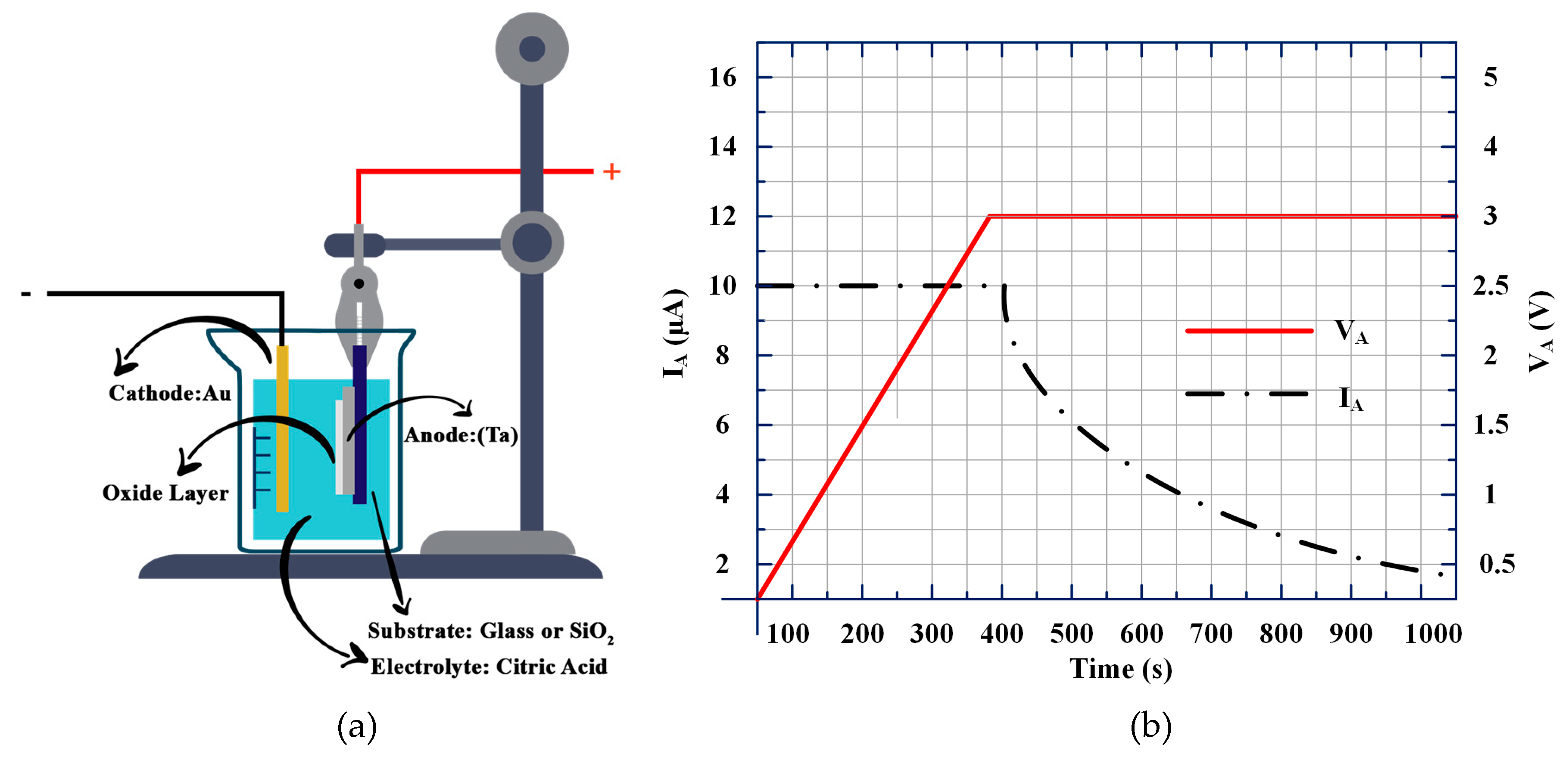
To optimise the dielectric performance of Ta
2O
5 and Ta
2O
5/OTS films, metal-insulator-metal (MIM) capacitors were fabricated. First, a 100 nm of Ta layer was deposited through a shadow mask by radio frequency (r.f.) magnetron sputtering to serve as the gate electrode. Sputtering was achieved by using a 2-inch diameter Ta target (99.99%) in Ar with a total pressure of 0.5 Pa. Next, samples were anodized in 1 mM of citric acid (≥ 99.5%, Sigma-Aldrich, St. Louis, MO, USA) using 99.99% pure Au wire as the cathode electrode as shown in
Figure 1a. To form tantalum oxide films of various thicknesses, anodization voltages (V
A) of 40, 30, 20, 10, 5 and 3 V with constant current density (0.01 mA/cm
2) were applied to the anode by Keithley 2400 Source Meter. The process was continued until the ionic current density dropped to 0.005 mA/cm
2. The variation of anodization voltage and current vs. time is depicted in
Figure 1b. Based on the anodization ratio of Ta reported in the literature [
19] ([c]
Ta = 2.2 nm/V), a 3 V anodized Ta should result in an approximately ~6.6 nm thick Ta
2O
5 layer. Some of the as-prepared Ta/Ta
2O
5 substrates were treated with O
2 plasma for 2 minutes and then immersed in a freshly prepared 1 mM solution of OTS in anhydrous toluene at room temperature for 30 minutes. Afterwards, the substrates were removed from the solution and rinsed thoroughly and without interruption with pure toluene in order to get rid of the excess of unreacted OTS. The treated substrates were thereafter annealed on a hot plate at 120 °C for 1 h under a flow of dry N
2. To obtain MIM capacitors, 50 nm thick Au electrodes were deposited onto the prepared Ta/Ta
2O
5 and Ta/Ta
2O
5/OTS films. The electrical characterization of the fabricated capacitors was carried out using an Agilent E4980A LCR meter. For the duration of the measurements, 1 V bias was applied to the bottom Ta electrode and the top Au electrode was grounded. Organic TFTs were fabricated in the bottom gate, top contact structure on an ultra-flat, quartz-coated glass substrate (S151, Ossila, Sheffield, UK). Poly(3,6-di(2-thien-5-yl)-2,5-di (2-octyldodecyl)-pyrrolo [3,4-c] pyrrole-1,4-dione) thieno [3,2-b] thiophene) (DPPDTT) and poly(methyl methacrylate) (PMMA) and their blend solutions were prepared according to the procedures reported elsewhere [
20]. In short, the DPPDTT-PMMA blend solution was prepared by separately dissolving 0.5 wt% DPPDTT and 0.5 wt% of PMMA in 1,2-dichlorobenzene (DCB) and subsequently mixed in a 7:3 ratio. Afterwards, the blend was stirred until completely mixed. The blend was then spin-coated at 2000 rpm for 2 min on substrates pre-heated at 100 °C. Subsequently, the deposited films were annealed at 100 °C for 30 min to 1 h under N
2 flow. Finally, a 100 nm thick layer of 99.99% Au was thermally evaporated through shadow masks to serve as a source and drain electrodes.
The channel width (W) and length (L) were 1 mm and 30 μm, respectively. The electrical characterization of the fabricated OTFTs was carried out using an Agilent E5270B semiconductor analyser (Santa Clara, CA, USA) and E4980A LCR meter (Keysight, Santa Rosa, CA, USA) at room temperature. The field-effect mobility is calculated by applying a linear fit to I
D1/2 vs V
G in the saturation regime using Equation (1):
where
VG is the gate voltage,
VT is the threshold voltage,
Ci is the gate capacitance density,
is saturation field-effect mobility, and
W and
L are channel width and length, respectively. All electrical measurements were done in ambient conditions in an electrically shielded, dark box.
3. Results and Discussions
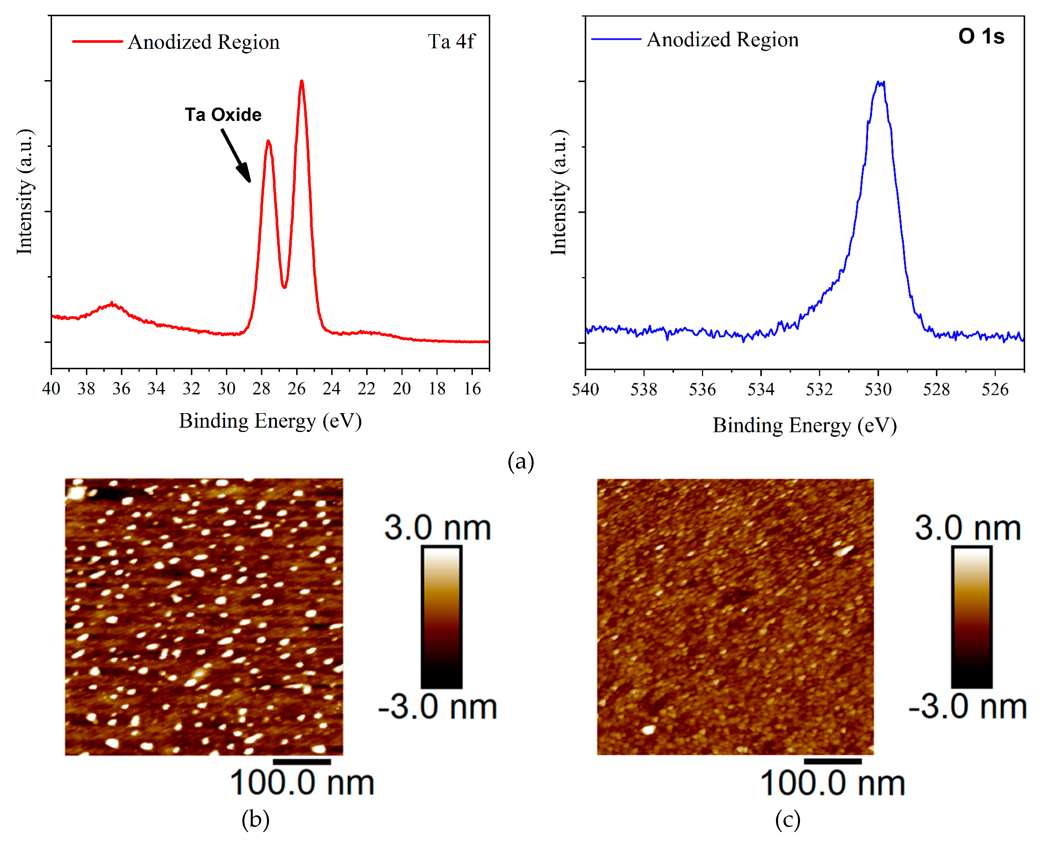
The presence of anodized tantalum oxide films was confirmed by X-ray photoelectron spectroscopy (XPS, Axis Ultra Hybrid, Kratos Analytical, Manchester, UK). A thick, i.e., thicker than the sampling depth of XPS, oxide was observed on the anodized region of the samples (see
Figure 2a and
Figures S1–S3 in the Supplementary Materials). By analysing the area of the Ta 4f and O 1s peaks, the Ta and O ratio was found to be nearly 2:5 confirming that tantalum pentoxide (Ta
2O
5) was successfully prepared through anodization. Also, as shown in
Figure 2a, the normalized O 1s peak fit indicates that the oxide formation on the anodized regions is consistent with the peak fitting analysis of the Ta 4f regions. To investigate the surface morphology of the anodized Ta
2O
5, atomic force microscope (AFM, Multimode, Bruker UK, Coventry, UK) images of the fabricated films have been taken.
Figure 2b,c show surface topography of both untreated and OTS-treated Ta
2O
5 films, respectively. The RMS roughness of untreated Ta
2O
5 film is 2.5 nm and the OTS-treated Ta
2O
5 1.3 nm. The tantalum oxide grown by anodization appears to be homogenous, uniform and fairly smooth. However, a more detailed AFM topographical analysis shows that OTS surface modification has made the oxide surface somewhat smoother when compared with as-prepared Ta
2O
5 films.
Figure 3 illustrates capacitance density, dielectric loss, leakage current and capacitance-voltage curves of anodized Ta
2O
5 films that were obtained at different anodization voltages, i.e., 40, 30, 20, 10, 5 and 3 V. In order to verify the measured values and test the devices’ fabrication reproducibility, all measurements were carried out on 20 randomly chosen devices out of the 100 different capacitors with Ta/Ta
2O
5/Au structure (cf. inset of
Figure 3a).
Figure 3 shows the response of one typical device out of the 20 studied devices.
Figure 3a depicts the capacitance density vs. frequency from 100 Hz to 100 kHz for the corresponding anodization voltages. As can be seen, for the dielectric thicknesses greater than ~22 nm (V
A = 10 V), capacitance density is relatively constant across the studied frequency range. As the Ta
2O
5 thickness decreases, it appears that the capacitors become unstable at both ends of the chosen frequency spectrum. Capacitors fabricated with Ta
2O
5 anodized at 40, 30, and 20 V exhibited an average capacitance density of 380, 450, and 700 nF/cm
2 at 1 kHz, respectively. The maximum standard deviation of the measured capacitance values for these capacitors was ±20 nF/cm
2.
On the other hand, the capacitors with anodic Ta
2O
5 prepared at 10, 5 and 3 V show much higher capacitances but also significantly higher leakage currents and dielectric losses, especially for V
A ≤ 5 V. As a result, we conclude that the pristine Ta
2O
5 films anodized at or below 10 V (d ~ 22 nm) are unsuitable for practical applications. Correspondingly, the dissipation factor (DF) measured on capacitors using Ta
2O
5 anodized at various voltages is depicted in
Figure 3b. For the simplest actual model, i.e., equivalent series resistance in series with the capacitance that neglects equivalent series inductance and insulation resistance, DF is the ratio of equivalent series resistance (ESR) and capacitive reactance (Xc), as written in Equation (2) [
21]:
Ideally, for a given capacitor DF should be zero, but practically it consists of a negligible loss due to resistive characteristics. As shown in
Figure 3b, the capacitors with 40, 30, and 20 V anodized Ta
2O
5 display a minimal DF that is close to zero. However, as the anodization voltage decreases below 20 V, DF becomes larger and the leakage currents through the anodic dielectric layer start to be appreciable (cf.
Figure 3b,c). Accordingly, as the Ta
2O
5 dielectric thickness decreases even further (V
A = 5 and 3 V) the leakage current through the dielectric becomes very large. In particular, capacitors with the thinnest anodic Ta
2O
5, i.e., anodized at 3 V, exhibit the largest leakage current density (J
L) 10
−3 A/cm
2 at 1 V. The same electronic behaviour of the anodized Ta
2O
5 can also be seen in the C–V characteristics of the corresponding capacitors shown in
Figure 3d, where high leakage currents reduce the voltage across the capacitors resulting in a lower electric field and lower capacitance at the positive end of the C–V curves. This is in contradiction with an ideal case, where a capacitor shows a flat capacitance-voltage characteristic which guarantees reliable and stable device performance. Nevertheless, thicker layers of Ta
2O
5 show flat and stable electrical behaviour across the chosen voltage characterization range. Based on the abovementioned dielectric characteristics, it appears that the minimum anodization voltage of tantalum for capacitor and TFT applications is 20 V, which corresponds to approximately 45 nm of Ta
2O
5. Indeed, the J
L for capacitors with 45 nm Ta
2O
5 layers is well below the maximum allowable value for TFT leakage current density (i.e., 10
−6 A/cm
2) and is measured to be 10
−7 A/cm
2 at 1 V.
Figure 4a shows the structure of the fabricated bottom-gate, top-contact Ta/(45 nm Ta
2O
5)/DPPDTT-PMMA/Au TFTs on a glass substrate (V
A = 20 V). Typical output and transfer characteristics of the fabricated transistors are shown in
Figure 4b, c, respectively. As can be seen in
Figure 4b, the drain current displays clear linear, pinch-off and saturation regions for all applied gate voltages.
The devices operate at 1 V with a saturation field-effect mobility of 0.02 cm
2 V
−1 s
−1, threshold voltage −0.35 V, subthreshold swing 210 mV/dec, and current on/off ratio ~10
3. This transistor performance is comparable to the previously reported organic TFTs that used SAM-modified, anodized Al
2O
3 [
22].
To see if the dielectric SAM modification strategy also results in improved transistor characteristics of the TFTs with anodized Ta
2O
5, DPPDTT-PMMA TFTs with OTS-modified tantalum pentoxide have been fabricated. OTS is one of the most used SAMs in organic transistors. It has been shown that OTS significantly improves dielectric/semiconductor interface by passivating the gate insulator surface that leads to the reduction of charge carrier traps, and as result, to higher charge carrier mobility [
23,
24]. During silanization, OTS molecules are attached to the dielectric surface through the chemical reaction of –SiCl with –OH groups on the metal oxide surface. This results in –Si–O–M structures. The other two –SiCl bonds of the OTS molecule react with proximate OTS molecules which forms a cross-linked monolayer. The OTS-treatment of the Ta
2O
5 layer inevitably results in a thicker overall dielectric layer, and hence decreases the overall areal capacitance of the dielectric film. The anodized Ta
2O
5 layer should be thin enough to provide the minimum required capacitance and leakage to operate the OTFTs at low voltage. Taking into account that the Ta native oxide thickness is about 3.5 nm [
25], it is believed that to suppress the effect of the native oxide on the dielectric properties of Ta
2O
5 the thickness of the anodized Ta should be at least 3.5 nm thick. As shown in
Figure 3a,c, an untreated Ta
2O
5 layer anodized at 3 V (d ~7 nm) exhibits a large enough areal capacitance to be able to operate DPPDTT-PMMA TFTs at 1 V. However, the very high leakage current density of these thin layers would lead to poor field-effect transistor characteristics if used as prepared.
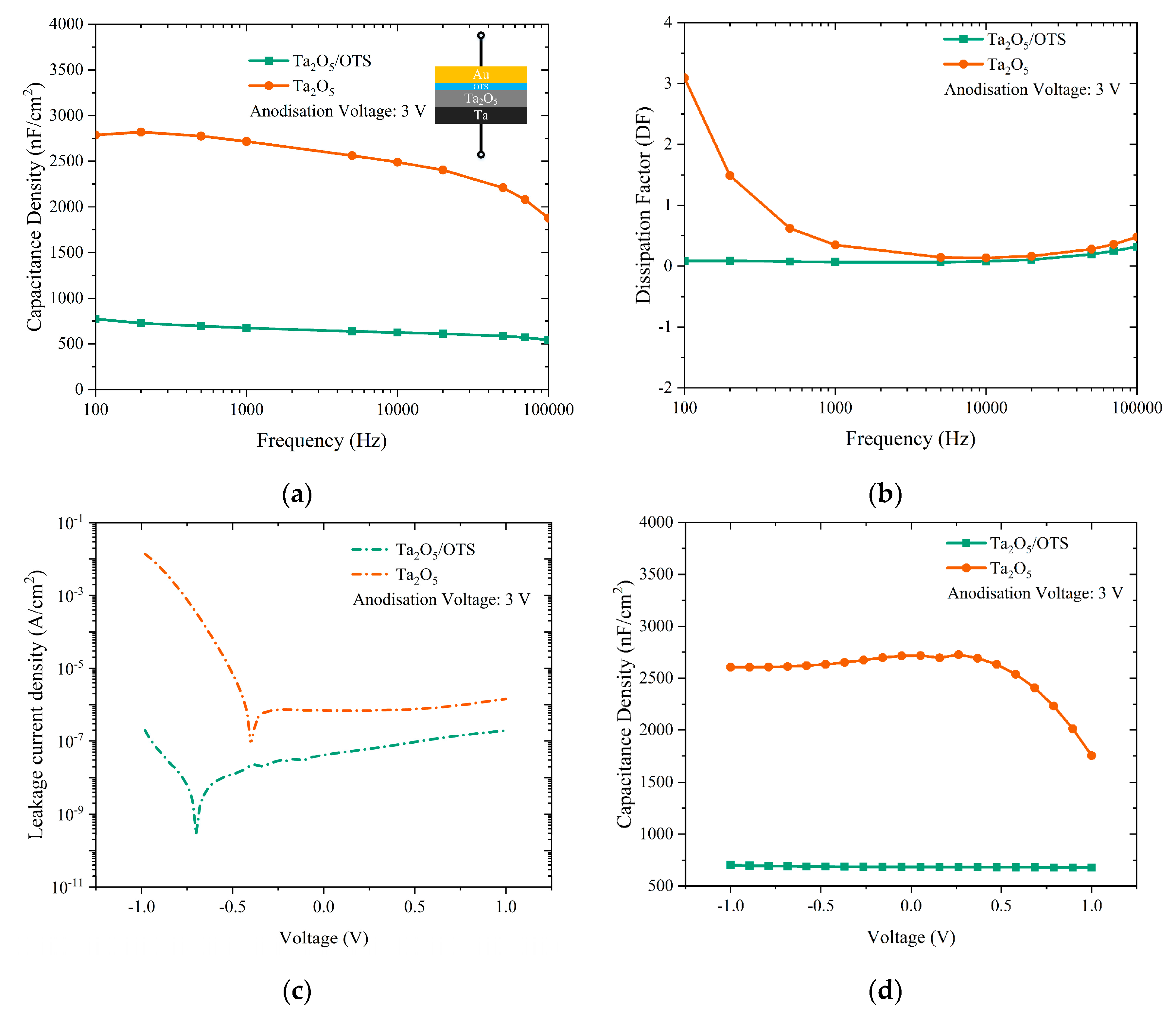
Figure 5a–d compare the dielectric properties of 3 V anodized untreated Ta
2O
5 and OTS-treated Ta
2O
5 films. As can be observed in
Figure 5a, the capacitance density of OTS-treated Ta
2O
5 is notably reduced from 2700 nF/cm
2 for bare Ta
2O
5 film to approximately 680 nF/cm
2. This is due to the addition of the OTS layer which leads to a thicker dielectric film and correspondingly smaller overall capacitance density because of two dielectric layers in series. Nonetheless, capacitance density curves for OTS-treated Ta
2O
5 are highly stable over a wide range of frequencies. The dielectric loss (
Figure 5b) for OTS-treated Ta
2O
5 shows negligible variation (less than 0.1) confirming a low defect density in the OTS-treated Ta
2O
5 films. As shown in
Figure 5c, leakage current density for OTS-treated Ta
2O
5 is approximately 2 × 10
−7A/cm
2 at ±1 V; this is reduced by circa five orders of magnitude at −1 V and circa one order of magnitude at +1 V when compared to films of untreated Ta
2O
5 of comparable thickness. The leakage current of the OTS-treated Ta
2O
5 is somewhat asymmetric and slightly lower for negative voltages. This is very likely caused by the use of electrodes with different work functions and differences in the roughness of the Ta/Ta
2O
5 and Ta
2O
5/OTS interfaces [
26]. In addition, as illustrated in
Figure 5d, in contrast to untreated Ta
2O
5, OTS surface modification has improved the stability of the capacitance density over the studied voltage range (−1 V to 1 V) and led to almost ideally flat C–V curves.
To test if the optimized, OTS-modified Ta
2O
5 layers result in well-working 1 V devices, glass/Ta/(7 nm Ta
2O
5)/OTS/DPPDTT-PMMA/Au OTFTs have been fabricated (V
A = 3 V). Typical output and transfer characteristics of the fabricated transistors are shown in
Figure 6b,c, respectively. The optimized devices operate at 1 V with virtually no hysteresis, the saturation field-effect mobility is 0.22 cm
2 V
−1 s
−1, the threshold voltage −0.55 V, subthreshold swing 120 mV/dec, and the current on/off ratio is in excess of 5 × 10
3. Additionally, the leakage current at −1 V is measured to be less than 1 nA at all applied biases. The calculated field-effect mobility for these devices is > 0.2 cm
2 V
−1 s
−1, ten times larger than the analogous DPPDTT-PMMA TFTs fabricated on bare Ta
2O
5. It is believed that charge carrier mobility in TFTs is directly affected by the interfacial trap density [
27]. Trap density in thin-film transistors can be calculated using Equation (3):
where
CG is the gate capacitance density,
q is the electron charge,
k is the Boltzmann’s constant,
T is the temperature, and
SS is subthreshold swing.
Nit is calculated to be 1.09 × 10
13 cm
−2 and 4.2 × 10
12 cm
−2 for OTFTs using 20 V, untreated Ta
2O
5 and 3 V, OTS-treated Ta
2O
5, respectively. The reduction of trap density confirms that the OTS layers shield the active layer from traps at the anodic Ta
2O
5/DPPDTT-PMMA interface.
Table 1 compares the key figures-of-merit of the 1 V OTFTs fabricated in this work in comparison with one-volt organic TFTs we reported previously [
22,
28,
29]. As can be seen, the gate capacitance density of the developed OTS-treated Ta
2O
5 dielectric layer used here is significantly higher. Importantly, other transistor parameters are comparable or indeed better than the parameters of the state-of-the-art organic TFTs reported to date [
30,
31,
32]. As a result, the demonstrated organic transistors are promising candidates for use in low-voltage, portable electronics.

 ,
, 


