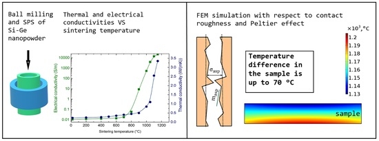
Simulation of Field Assisted Sintering of Silicon Germanium Alloys

 , ,
, ,
Abstract
:
1. Introduction
2. Materials and Methods
3. Modeling
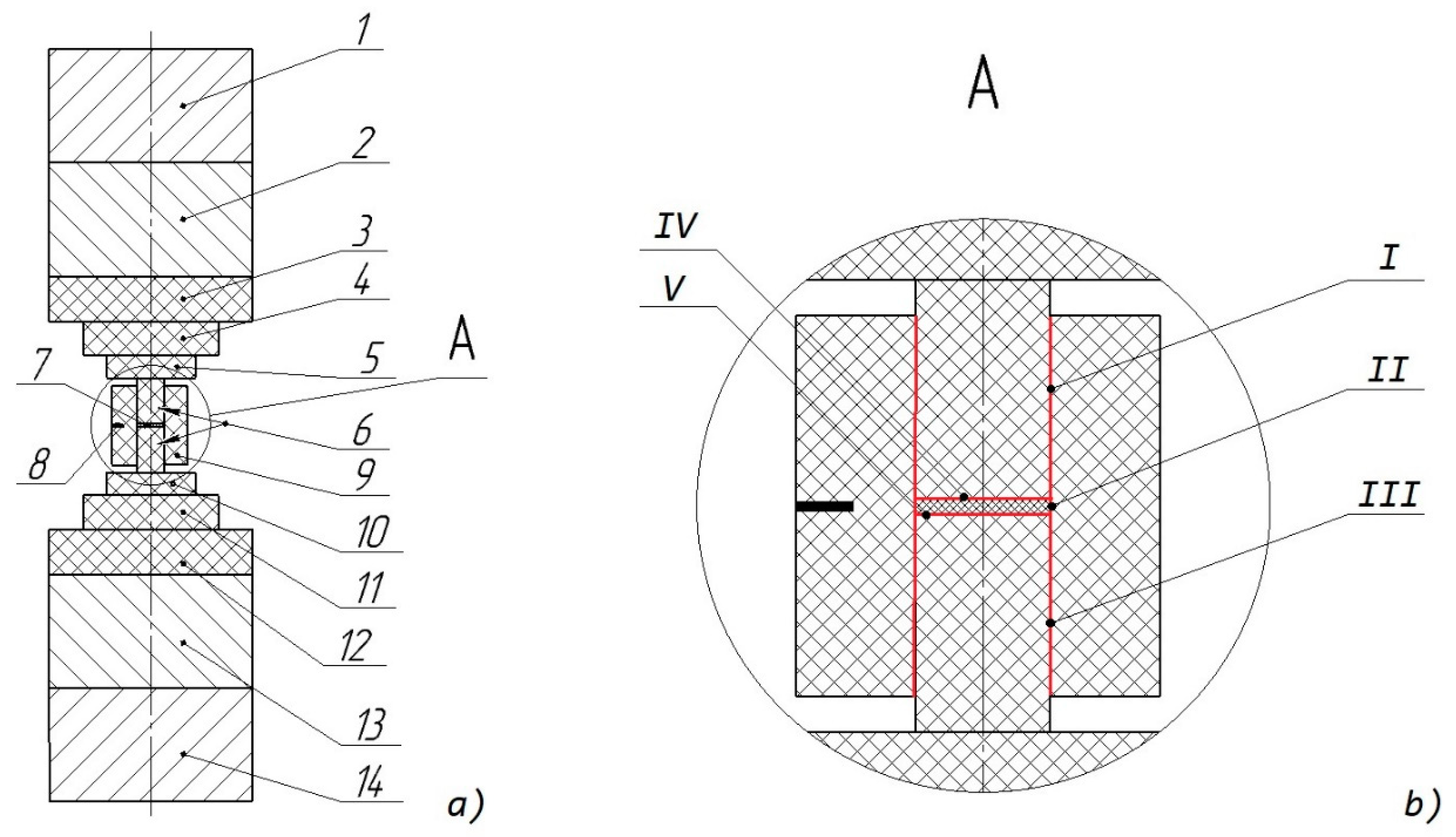
3.1. Geometry
3.2. Mathematical Description
3.2.1. Electrical and Thermal Processes
3.2.2. Mechanical Processes
3.2.3. Electrical and Thermal Contacts
3.2.4. Electric Boundary Conditions
3.2.5. Thermal Boundary Conditions
3.2.6. Mechanical Boundary Conditions
3.2.7. Mesh
4. Simulation Results and Discussion
4.1. Temperature and Current in the Sample and Setup Elements
4.2. Contact Resistance and Its Impact on the Temperature
5. Conclusions
Author Contributions
Funding
Conflicts of Interest
References
- Fitriani, O.R.; Long, B.D.; Barma, M.C.; Riaz, M.; Sabri, M.F.M.; Said, S.M.; Saidur, R. A review on nanostructures of high-temperature thermoelectric materials for waste heat recovery. Adv. Mater. Res. Switz. 2016, 64, 635–659. [Google Scholar] [CrossRef]
- Murugasami, R.; Vivekanandhan, P.; Kumaran, S.; Suresh Kumar, R.; Tharakan, T.J. Densification and alloying of ball milled Silicon-Germanium powder mixture during spark plasma sintering. Adv. Powder Technol. 2017, 28, 506–513. [Google Scholar] [CrossRef]
- Usenko, A.A.; Moskovskikh, D.O.; Gorshenkov, M.V.; Korotitskiy, A.V.; Kaloshkin, S.D.; Voronin, A.I.; Khovaylo, V.V. Optimization of ball-milling process for preparation of Si-Ge nanostructured thermoelectric materials with a high figure of merit. Scripta Mater. 2015, 96, 9–12. [Google Scholar] [CrossRef]
- Usenko, A.; Moskovskikh, D.; Gorshenkov, M.; Voronin, A.; Stepashkin, A.; Kaloshkin, S.; Arkhipov, D.; Khovaylo, V. Enhanced thermoelectric figure of merit of p-type Si0.8Ge0.2 nanostructured spark plasma sintered alloys with embedded SiO2 nanoinclusions. Scripta Mater. 2017, 127, 63–67. [Google Scholar] [CrossRef]
- Usenko, A.; Moskovskikh, D.; Korotitskiy, A.; Gorshenkov, M.; Zakharova, E.; Fedorov, A.; Parkhomenko, Y.; Khovaylo, V. Thermoelectric properties and cost optimization of spark plasma sintered n-type Si0.9Ge0.1-Mg2Si nanocomposites. Scripta Mater. 2018, 146, 295–299. [Google Scholar] [CrossRef]
- Joshi, G.; Lee, H.; Lan, Y.C.; Wang, X.W.; Zhu, G.H.; Wang, D.Z.; Gould, R.W.; Cuff, D.C.; Tang, M.Y.; Dresselhaus, M.S.; Chen, G.; Ren, Z.F. Enchanced thermoelectric figure-of-merit in nanostructured p-type silicon germanium bulk alloys. Nano Lett. 2008, 8, 4670–4674. [Google Scholar] [CrossRef]
- Lan, Y.; Minnich, A.J.; Chen, G.; Ren, Z. Enhancement of thermoelectric figure-of-merit by a bulk nanostructuring approach. Adv. Funct. Mater. 2010, 20, 357–376. [Google Scholar] [CrossRef]
- He, J.; Tritt, T.M. Advances in thermoelectric materials research: Looking back and moving forward. Science 2017, 357, 1369–1378. [Google Scholar] [CrossRef]
- Wang, X.W.; Lee, H.; Lan, Y.C.; Zhu, G.H.; Joshi, G.; Wang, D.Z.; Yang, J.; Muto, A.J.; Tang, M.Y.; Klatsky, J.; Song, S.; Dresselhaus, M.S.; Chen, G.; Ren, Z.F. Enhanced thermoelectric figure of merit in nanostructured n-type silicon germanium bulk alloy. Appl. Phys. Lett. 2008, 93, 193121. [Google Scholar] [CrossRef]
- Bera, C.; Soulier, M.; Navone, C.; Roux, G.; Simon, J.; Volz, S.; Mingo, N. Thermoelectric properties of nanostructured Si1-xGex and potential for further improvement. J. Appl. Phys. 2010, 108, 124306. [Google Scholar] [CrossRef]
- Minnich, A.J.; Dresselhaus, M.S.; Ren, Z.F.; Chen, G. Bulk nanostructured thermoelectric materials: Current research and future prospects. Energy Environ. Sci. 2009, 2, 466–479. [Google Scholar] [CrossRef]
- Poudel, B.; Hao, Q.; Ma, Y.; Lan, Y.; Minnich, A.; Yu, B.; Yan, X.; Wang, D.; Muto, A.; Vashaee, D.; Chen, X.; Liu, J.; Dresselhaus, M.S.; Chen, G.; Ren, Z. High-thermoelectric performance of nanostructured bismuth antimony telluride bulk alloys. Science 2008, 320, 634–638. [Google Scholar] [CrossRef]
- Dresselhaus, M.S.; Chen, G.; Tang, M.Y.; Yang, R.; Lee, H.; Wang, D.; Ren, Z.; Fleurial, J.-P.; Gogna, P. New directions for low-dimensional thermoelectric materials. Adv. Mater. 2007, 19, 1043–1053. [Google Scholar] [CrossRef]
- Dmitriev, A.V.; Zvyagin, I.P. Current trends in the physics of thermoelectric materials. Phys. Usp. 2010, 53, 789–803. [Google Scholar] [CrossRef]
- Bulat, L.P.; Bublik, V.T.; Drabkin, I.A.; Karataev, V.V.; Osvenskii, V.B.; Parkhomenko, Y.N.; Pivovarov, G.I.; Pshenai-Severin, D.A.; Tabachkova, N.Y. Bulk nanostructured polycrystalline p-Bi-Sb-Te thermoelectrics obtained by mechanical activation method with hot pressing. J. Electron. Mater. 2010, 39, 1650–1653. [Google Scholar] [CrossRef]
- Bulat, L.P.; Drabkin, I.A.; Karatayev, V.V.; Osvenskii, V.B.; Parkhomenko, Y.N.; Pshenai-Severin, D.A.; Sorokin, A.I. The influence of anisotropy and nanoparticle size distribution on the lattice thermal conductivity and the thermoelectric figure of merit of nanostructured (Bi,Sb)2Te3. J. Electron. Mater. 2014, 43, 2121–2126. [Google Scholar] [CrossRef]
- Goldsmid, H.J. Introduction to Thermoelectricity; Springer-Verlag: Heidelberg, Germany, 2016; pp. 74–76. [Google Scholar]
- Vining, C.B. A model for the high-temperature transport properties of heavily doped n-type silicon-germanium alloys. J. Appl. Phys. 1991, 69, 331–341. [Google Scholar] [CrossRef]
- Slack, G.A.; Moayyed, A.H. The maximum possible conversion efficiency of silicon-germanium thermoelectric generators. J. Appl. Phys. 1991, 70, 2694–2718. [Google Scholar] [CrossRef]
- Bulat, L.P.; Osvenskii, V.B.; Parkhomenko, Y.N.; Pshenai-Severin, D.A. Investigation of the possibilities for increasing the thermoelectric figure of merit of nanostructured materials based on Bi2Te3-Sb2Te3 solid solutions. Phys. Solid State 2012, 54, 2165–2172. [Google Scholar] [CrossRef]
- Liu, W.; Ren, Z.; Chen, G. Nanostructures thermoelectric materials. In Thermoelectric Nanomaterials; Koumoto, K., Mori, T., Eds.; Springer Series in Materials Science Vol. 182; Springer-Verlag: Heidelberg, Germany, 2013; pp. 255–286. [Google Scholar]
- Suárez, M.; Fernández, A.; Menéndez, J.L.; Torrecillas, R.; Kessel, H.U.; Hennicke, J.; Kirchner, R.; Kessel, T. Challenges and opportunities for spark plasma sintering: A key technology for a new generation of materials. In Sintering Applications; Ertug, B., Ed.; IntechOpen: Burcu Ertuğ, Turkey, 2013; Chapter 13; pp. 319–342. [Google Scholar]
- Guillon, O.; Gonzalez-Julian, J.; Dargatz, B.; Kessel, T.; Schierning, G.; Rathel, J.; Herrmann, M. Field-assisted sintering technology/spark plasma sintering: Mechanisms, materials, and technology developments. Adv. Eng. Mater. 2014, 16, 830–849. [Google Scholar] [CrossRef]
- Zavaliangos, A.; Zhang, J.; Krammer, M.; Groza, J.R. Temperature evolution during field activated sintering. Mater. Sci. Eng. A 2004, 379, 218–228. [Google Scholar] [CrossRef]
- Achenani, Y.; Saadaoui, M.; Cheddadi, A.; Bonnefont, G.; Fantozzi, G. Finite element modeling of spark plasma sintering: Application to the reduction of temperature inhomogeneities, case of alumina. Mater. Des. 2017, 116, 504–514. [Google Scholar] [CrossRef]
- Giovanni, M.; Mastrorillo, G.D.; Grasso, S.; Ning, H.; Reece, M.J. Peltier effect during spark plasma sintering (SPS) of thermoelectric materials. J. Mater. Sci. 2017, 52, 10341–10352. [Google Scholar] [CrossRef]
- Kim, Y.; Shin, C.; Kim, T.; Kang, S.-W. Inhomogeneity in thermoelectrics caused by Peltier effect-induced temperature gradient during spark plasma sintering. Scripta Mater. 2019, 158, 46–49. [Google Scholar] [CrossRef]
- Schwertz, M.; Katz, A.; Sorrel, E.; Lemonnier, S.; Barraud, E.; Carradò, A.; d’Astorg, S.; Leriche, A.; Nardin, M.; Vallat, M.F.; Kosior, F. Coupled electro-thermo-mechanical finite element modeling of the spark plasma sintering technique. Metall. Mater. Trans. B 2016, 47, 1263–1273. [Google Scholar] [CrossRef]
- Maniere, C.; Durand, L.; Weibel, A.; Estournes, C. Spark-plasma-sintering and finite element method: From the identification of the sintering parameters of a submicronic α-alumina powder to the development of complex shapes. Acta Mater. 2016, 102, 169–175. [Google Scholar] [CrossRef]
- Anselmi-Tamburinia, U.; Gennarib, S.; Garaya, J.E.; Munir, Z.A. Fundamental investigations on the spark plasma sintering/synthesis process II. Modeling of current and temperature distributions. Mater. Sci. Eng. A 2005, 394, 139–148. [Google Scholar] [CrossRef]
- Pavia, A.; Durand, L.; Ajustiron, F.; Bley, V.; Chevallier, G.; Peigney, A.; Estournes, C. Electro-thermal measurements and finite element method simulations of a spark plasma sintering device. J. Mater. Process. Tech. 2013, 213, 1327–1336. [Google Scholar] [CrossRef] [Green Version]
- Charles, M.; Pavia, A.; Durand, L.; Chevallier, G.; Afanga, K.; Estournes, C. Finite-element modeling of the electro-thermal contacts in the spark plasma sintering process. J. Eur. Ceram. Soc. 2016, 36, 741–748. [Google Scholar] [CrossRef] [Green Version]
- Gladden, J.R.; Li, G.; Adebisi, R.; Firdosy, S.; Caillat, T.; Ravi, V. High-temperature elastic moduli of bulk nanostructured n- and p-type silicon germanium. Phys. Rev. B 2010, 82, 045209. [Google Scholar] [CrossRef]
- Kim, H.S. Densification modelling for nanocrystalline metallic powders. J. Mater. Process. Tech. 2003, 140, 401–406. [Google Scholar] [CrossRef]
- Fedotov, A. Analysis of the adequacy and selection of phenomenological models of the elastic properties of porous powder materials. J. Mater. Sci. 2017, 52, 2964–2973. [Google Scholar] [CrossRef]
- Song, Y.; Li, Y.; Zhou, Z.; Lai, Y.; Ye, Y. A multi-field coupled FEM model for one-step-forming process of spark plasma sintering considering local densification of powder material. J. Mater Sci. 2011, 46, 5645–5656. [Google Scholar] [CrossRef]
- Zhdanovich, G.M. Theory of Compacting of Metal Powders; Metallurgy: Moscow, Russia, 1969; pp. 1–264. [Google Scholar]
- Zhang, J. Numerical simulation of thermoelectric phenomena in field activated sintering. Ph.D. Thesis, Drexel University, Philadelphia, PA, USA, 2004. [Google Scholar]
- Vanmeensel, K.; Laptev, A.; Vleugels, J.; Van Der Biest, O. Modelling of the temperature distribution during field assisted sintering. Acta Mater. 2005, 53, 4379–4388. [Google Scholar] [CrossRef]
- McWilliams, B.A. Numerical simulation of electric field assisted sintering. Ph.D. Thesis, Drexel University, Philadelphia, PA, USA, 2008. [Google Scholar]
- Construction Materials Factory “Technocarb”. Available online: http://technocarb.ru/catalog/structural-graphite/mpg/ (Accessed on 14 January 2019).
- Yovanovich, M.M.; Marotta, E.E. Thermal Spreading and Contact Resistance. In Heat Transfer Handbook; Bejan, A., Kraus, A.D., Eds.; John Wiley & Sons: New York, NY, USA, 2003; pp. 261–393. [Google Scholar]
- Shin, D.K.; Jang, K.W.; Ur, S.C.; Kim, I.H. Thermoelectric Properties of Higher Manganese Silicides Prepared by Mechanical Alloying and Hot Pressing. J. Electron. Mater. 2013, 42, 1756–1761. [Google Scholar] [CrossRef]


© 2019 by the authors. Licensee MDPI, Basel, Switzerland. This article is an open access article distributed under the terms and conditions of the Creative Commons Attribution (CC BY) license (http://creativecommons.org/licenses/by/4.0/).
Share and Cite
Tukmakova, A.; Novotelnova, A.; Samusevich, K.; Usenko, A.; Moskovskikh, D.; Smirnov, A.; Mirofyanchenko, E.; Takagi, T.; Miki, H.; Khovaylo, V. Simulation of Field Assisted Sintering of Silicon Germanium Alloys. Materials 2019, 12, 570. https://doi.org/10.3390/ma12040570
Tukmakova A, Novotelnova A, Samusevich K, Usenko A, Moskovskikh D, Smirnov A, Mirofyanchenko E, Takagi T, Miki H, Khovaylo V. Simulation of Field Assisted Sintering of Silicon Germanium Alloys. Materials. 2019; 12(4):570. https://doi.org/10.3390/ma12040570
Chicago/Turabian StyleTukmakova, Anastasiia, Anna Novotelnova, Kseniia Samusevich, Andrey Usenko, Dmitriy Moskovskikh, Alexandr Smirnov, Ekaterina Mirofyanchenko, Toshiyuki Takagi, Hiroyuki Miki, and Vladimir Khovaylo. 2019. "Simulation of Field Assisted Sintering of Silicon Germanium Alloys" Materials 12, no. 4: 570. https://doi.org/10.3390/ma12040570