Article

The Optoelectronic Properties of p-Type Cr-Deficient Cu[Cr0.95−xMg0.05]O2 Films Deposited by Reactive Magnetron Sputtering

1
The Key Lab of Guangdong for Modern Surface Engineering Technology, National Engineering Laboratory for Modern Materials Surface Engineering Technology, Guangdong Institute of New Materials, Guangzhou 510651, China
2
Shandong Key Laboratory of Optical Astronomy and Solar-Terrestrial Environment, School of Space Science and Physics, Shandong University, Weihai 264209, China
3
Department of Materials Engineering and Center for Plasma and Thin Film Technologies, Ming Chi University of Technology, Taipei 243, Taiwan
4
College of Engineering, Chang Gung University, Taoyuan 333, Taiwan
5
Institute of Materials Science and Engineering, National Taiwan University, Taipei 106, Taiwan
6
School of Materials Science and Engineering, Southwest Jiaotong University, Chengdu 610031, China
*
Author to whom correspondence should be addressed.
Materials 2020, 13(10), 2376; https://doi.org/10.3390/ma13102376
Submission received: 19 April 2020 / Revised: 7 May 2020 / Accepted: 18 May 2020 / Published: 21 May 2020

Abstract

:
CuCrO2 is one of the most promising p-type transparent conductive oxide (TCO) materials. Its electrical properties can be considerably improved by Mg doping. In this work, Cr-deficient CuCrO2 thin films were deposited by reactive magnetron sputtering based on 5 at.% Mg doping. The influence of Cr deficiency on the film’s optoelectronic properties was investigated. As the film’s composition varied, CuO impurity phases appeared in the film. The mixed valency of Cu+/Cu2+ led to an enhancement of the hybridization between the Cu3d and O2p orbitals, which further reduced the localization of the holes by oxygen. As a result, the carrier concentration significantly improved. However, since the impurity phase of CuO introduced more grain boundaries in Cu[Cr0.95−xMg0.05]O2, impeding the transport of the carrier and incident light in the film, the carrier mobility and the film’s transmittance reduced accordingly. In this work, the optimal optoelectronic performance is realized where the film’s composition is Cu[Cr0.78Mg0.05]O2. Its Haacke’s figure of merit is about 1.23 × 10⁻⁷ Ω−1.

1. Introduction

Transparent conductive oxides (TCOs) combine good conductivity and ideal transmittance and can be used in various domains [1,2,3]. However, most commercially used TCOs are n-type conductivity in which the majority carriers are electrons [4]. In fact, most oxides are intrinsic n-type conductive semiconductors. Due to the self-compensation effect, the p-type conductivity obtained by doping in n-type TCOs is unstable [5,6]. Meanwhile, for the limited intrinsic p-type oxides, since the valence band maximum is mainly occupied by O2p orbital, the strong electron negativity of oxygen ions localizes holes around them, resulting in a decrease in the carrier concentration and carrier mobility [7,8]. Thus, their p-type conductivity is generally poor. For the above reasons, p-type TCOs with ideal optoelectronic performance are difficult to fabricate [9,10,11]. p-type TCOs are an essential part in the building of fully transparent electronic devices and also play an imperative role as hole transport layers (HTLs) in novel perovskite solar cells and hole injection layers in organic light-emitting diode (OLED) displays [12,13,14]. In this context, lots of effort has been paid to developing p-type TCOs. Copper oxides are considered to be promising p-type TCOs [15,16]. The hybridization between Cu3d and O2p orbits effectively reduces the localization of the holes by oxygen ions, which is beneficial to improving the p-type conductivity of TCOs [17]. In particular, in 2001, Tate et al. reported that the conductivity of delafossite CuCrO2 film doped with Mg can reach 220 S·cm−1, which makes p-type TCOs present optimistic application prospects [18]. However, the film’s corresponding transmittance in the visible region is around just 30%.
Delafossite oxides have been widely studied in the past few decades. The conductivity of undoped delafossite materials is not very good [19]. However, their carrier concentration can be effectively enhanced using the doping method, thereby improving their electrical property [20,21]. Fang et al. analyzed the extrinsic defects in CuCrO2 using the first-principles methods and found that for all the acceptor-type extrinsic defects, substituting Mg for Cr is the most prominent doping acceptor with relatively shallow transition energy levels in CuCrO2 [22]. Its conductive mechanism can be depicted by the following equation:
( C r C r ) × + M g ( M g C r ) + Cr + h +
where (CrCr)× represents the Cr in the original lattice sites, (MgCr)’ represents the Mg2+ in Cr3+ site and h+ is the positive hole. To date, the highest p-type conductivity of about 278 S·cm−1 has been obtained in Mg and N co-doped CuCrO2 film deposited by radiofrequency (RF) sputtering, where the Cu vacancies (VCu) as well as the substitution of Cr by Mg (MgCr) and O by N (NO) are considered as the intrinsic acceptor and extrinsic acceptor, respectively [23]. All of them contribute to the carrier concentration. Generally, a Cu-deficient condition is considered easier to generate Cu vacancy and is in favor of the film’s p-type conductivity. However, Chen et al. reported that Cr-deficient conditions can realize higher carrier concentrations [24]. This is because where Cr is deficient, Cu atoms in the structure might occupy Cr sites to form anti-site (CuCr) defects, leading to increased hole concentration. This process can be described as the following:
( C u C u ) × + ( C r C r ) × ( V C u ) + ( C u C r ) + 3 h
where (CuCu)× and (CrCr)× represent the Cu and Cr in their original lattice sites, (VCu) is the Cu vacancy, (CuCr) is the Cu in Cr site and h is the compensated hole. As a result, the film’s p-type conductivity is improved. Other works also support this conclusion [25]. So far, there is no report about reinforcement of the optoelectronic properties of CuCrO2 thin films by Mg doping and the introduction of Cr deficiency at the same time. Thus, in this work, Mg doped Cr-deficient CuCrO2 films were deposited in order to optimize the p-type conductivity of CuCrO2. The influence of Cr content on the film’s optoelectronic properties is discussed in detail.

2. Materials and Methods

Mg doped Cr-deficient CuCrO2 films with a thickness of about 350 nm were deposited by reactive magnetron sputtering with direct current (DC) power supply at room temperature. This method allows perfect control of the film’s composition and possesses a higher deposition rate compared to RF sputtering. p-type silicon (100) wafer and fused quartz were used as substrates. Before the deposition, the substrates were ultrasonically cleaned successively using ultrapure water, acetone and alcohol for 15 min, initially. After cleaning, the residual alcohol on the substrates was blow-dried using a high-purity nitrogen gas. Pure copper, chromium and magnesium targets (99.99% in purity) each with a 50.8 mm diameter and 3 mm thickness were powered by pulsed DC supplies. Before the deposition, the background of the reactive chamber was pre-pumped to 10−5 Pa. Then, a gas mixture of Ar + O2 was introduced into the chamber. The flow rate was fixed at 90 and 10 sccm, with the working pressure fixed at 0.9 Pa. During the deposition, the pulsed frequency of each power supply was fixed at 50 kHz, while the pulse off-time was maintained at 5 μs. The discharge current applied on the Cu, Cr, Mg targets was varied as 0.14–0.15 A, 0.90–0.98 A, 0.28–0.32 A (the corresponding sputtering powers were 29–32 W, 241–257 W, 27–32 W) in order to deposit the films with various compositions. The deposition rate was about 5.5–6.0 nm/min. Herein, all the Cr-deficient films were Cu stoichiometric with 5 at.% Mg doping. Meanwhile, Cr content varied from 0.95 to 0.58. Thus, the chemical formulas of all films can be written as Cu[Cr0.95−xMg0.05]O2, where the x values are 0.00, 0.09, 0.17, 0.23, and 0.37, respectively. Finally, all the films were annealed at 1023 K in a vacuum for 30 min in order to obtain a well crystallized delafossite structure.
The film’s thickness was determined by a surface profilometer (Ambios Technology Company, Santa Cruz, NM, USA). The film’s composition was confirmed by energy-dispersive spectroscopy (EDS, Nova Nano SEM 450, Hillsboro, OR, USA). The phase structures were analyzed by an X-ray diffractometer (XRD, Bruker D8 ADVANCE, Karlsruhe, Germany). Hall effect analysis with van der Pauw’s configuration (Keithley-4200 SCS, Beaverton, OR, USA) was used to investigate the film’s electrical properties under room temperature. The geometrical size of the rectangular sample is 1 cm × 1 cm. Finally, the film’s optical properties in the visible region and near infrared region were characterized by a UV-Vis spectrophotometer (Shimadzu UV-3600, Kyoto, Japan).

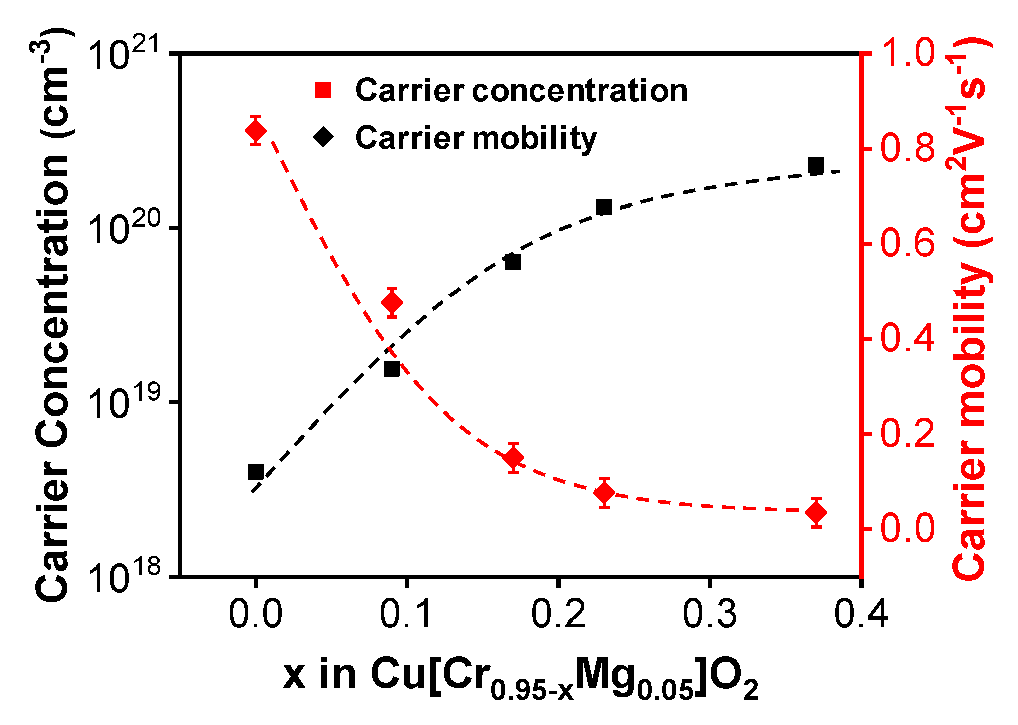
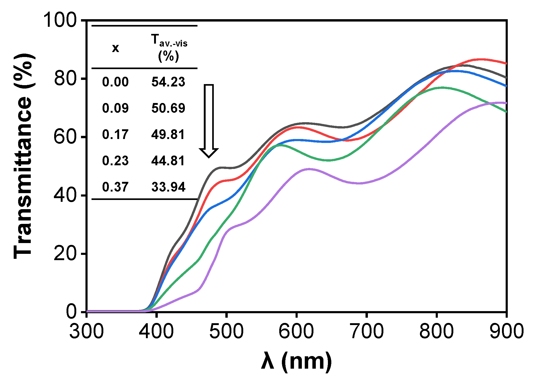
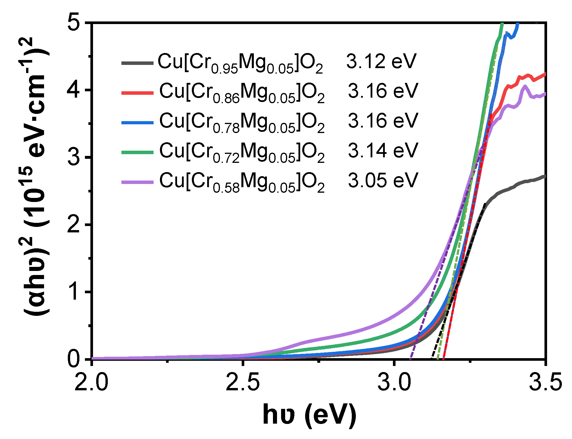
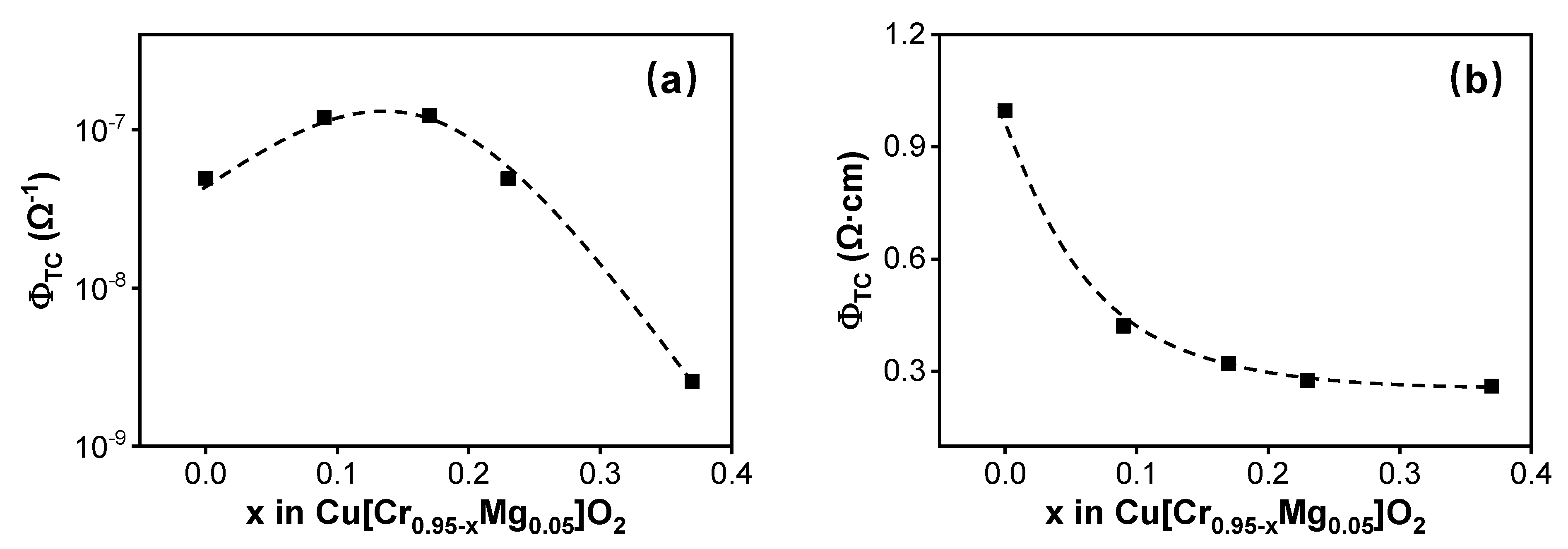
3. Results and Discussion

The XRD patterns of Cr-deficient Cu[Cr0.95−xMg0.05]O2 films are compared in Figure 1. The diffraction peaks at 36.8°, 41.7°, 42.8°, 47.9°, and 74.3° corresponded to the (006), (101), (012), (104), and (110) orientations of 3R-CuCrO2 delafossite structure (JCPDS: 89-0539), respectively. With the decrease in Cr content, the preferred orientation changed from (006) to (012) plan. It is pointed out that the growth of CuCrO2 along the c-axis was beneficial to improving its conductivity [26]; however, in 3R-CuCrO2, the (012) plan owned lower surface energy. Therefore, the Cr-deficient condition in the current work is more conducive to the growth of CuCrO2 within thermodynamic equilibrium conditions. Moreover, as Cr content decreased to 0.58, a CuO phase emerged. Daou et al. reported that the substitution of Cr3+ by Mg2+ in CuCrO2 could lead to the formation of CuO (as Mg content above 0.04) [27]. As a result, a mixed valency of Cu+/Cu2+ was induced by the Mg2+ substitution on the Cr3+ site. In fact, increasing Cr deficiency by either reducing the Cr content or replacing Cr with Mg caused a conversion of monovalent Cu to divalent Cu. This was corroborated by XANES (X-ray absorption near-edge structure) spectra theoretical calculation [28]. This behavior changed the densities of Cu3d, Cu3d–O2p and O2p states at or near the valence-band maximum or the Fermi level, which further affected the film’s p-type conductivity.
The films’ electrical properties were analyzed by Hall measurement. All the films with various compositions presented p-type conductivity. The variation of the carrier concentration and carrier mobility as a function of Cr content is shown in Figure 2. It can be seen that as Cr deficiency increased, the carrier concentration increased. As mentioned above, after the substitution of Cr3+ by Mg2+, monovalent Cu converted into divalent Cu. This resulted in an enhancement of the hybridization between Cu3d and O2p orbitals [25]. As a result, the localization effect of the holes by oxygen was diminished, and the hole carriers were thereby released around the Cu sites. Chen et al. reported that under Cr-deficient condition, Cu atoms can occupy Cr sites and form (CuCr) anti-site defects [24]. During this process, Cu vacancies as well as three holes are generated, as shown in Equation (2) mentioned before. As a consequence, the carrier concentration is significantly enhanced from 4.0 × 1018 cm−3 to 2.3 × 1020 cm−3 as Cr content decreases from 0.95 to 0.58. It can be seen that Cu[Cr0.95−xMg0.05]O2 becomes degenerate as the carrier concentration increases [29].
As for the carrier mobility, its variation is affected by two factors. On the one hand, at high Cr-deficient level, a CuO phase appears. The mixed valency of Cu+/Cu2+ results in an enhancement of the hybridization between Cu3d and O2p orbitals, which reduces the localization of the holes by oxygen and leads to a high carrier mobility [30]. On the other hand, the appearance of CuO impurity phase enhances the grain boundary scattering and thereby reduces the carrier mobility. In this work, the carrier mobility reduced from 0.84 to 0.04 cm2·V−1·s−1 as Cr content decreased from 0.95 to 0.58, indicating the grain boundary scattering plays a dominant role in the carrier mobility variation.
The electrical conductivity of Cr-deficient Cu[Cr0.95−xMg0.05]O2 films as a function of Cr content is shown in Figure 3. Under the combined effect of carrier concentration and carrier mobility, the film’s conductivity firstly increased and then decreased. This implies that, under high Cr-deficient level, the negative influence of the grain boundary scattering from CuO impurity phase exceeded the contribution of Cu2+ to the carrier concentration. Then, among the five samples prepared in the current work, the optimal p-type conductivity of about 1.63 S·cm−1 is achieved in Cu[Cr0.72Mg0.05]O2 film, where the carrier concentration and carrier mobility are 1.3 × 1020 cm−3 and 0.08 cm2·V−1·s−1, respectively.
The film’s transmittance variation in the visible region (400–800 nm) is shown in Figure 4. The average transmittance in the visible region was obtained with the following equation [31]:
T a v e r a g e = λ 1 λ n T ( λ ) d λ λ n λ 1 1 m λ = λ 1 m T ( λ )   ( m = λ 1 , λ 2 , λ 3 λ n )
where λ1 = 400 nm and λn = 800 nm. It clearly shows that the film’s transmittance reduces when Cr- deficiency increases. This phenomenon may be caused by the variation of the film’s crystallinity and the appearance of a CuO impurity phase. More light scattering is introduced into the film, thus reducing the film’s transmittance. As for the stoichiometric Cu[Cr0.95Mg0.05]O2 film, its average transmittance in the visible region amounts to 54.23%.
The optical band gap Eg of Cu[Cr0.95−xMg0.05]O2 can be estimated by the following formulas [32,33]:
α = 1 d ln ( 1 R T )
( α h v ) 1 / n = A ( h v E g )
where d is film thickness, R and T are optical reflectance and transmittance, respectively. is the incident photon energy, A is a constant and the exponent n depends on the type of transition: n = 1/2 and 2 for direct and indirect transition, respectively. Since CuCrO2 has a direct band gap transition, n equals 1/2 in this equation. Figure 5 depicts the variation of the direct band gap ( E g d ) of Cu[Cr0.95−xMg0.05]O2 film. As Cr content decreased from 0.95 to 0.86, 0.78, 0.72 and 0.58, the film’s corresponding direct band gap varied from 3.12 to 3.16, 3.16, 3.14, and 3.05 eV. At first, the increment in the film’s band gap was primarily caused by the Burstein–Moss effect, which is often found in degenerate semiconductors [31]. In the present work, as Cr deficiency increased, the Cu[Cr0.95−xMg0.05]O2 films became degenerate as the carrier concentration was higher than 1019 cm−3 [29]. Meanwhile, the Fermi level of Cu[Cr0.95−xMg0.05]O2 moved towards the valence band. In this condition, only electrons below the Fermi level can be excited to the conduction band because no states above the Fermi level are filled with electrons. As a result, the Burstein–Moss effect led to a greater band gap. This behavior is more pronounced in the Cr-deficient film, where the carrier concentration was higher than others. Thus, the film’s band gap became wider with increasing Cr deficiency. Similar behavior has also been reported in other works [34,35]. However, as Cr deficiency further increased, the film’s band gap narrowed when a CuO phase appears. This was mainly caused by the narrower band gap of CuO of about 1.25 eV greatly enhancing light absorption [36]. As a result, the film’s band gap reduced. Considering the debate over the nature of the band gap of CuCrO2 [37], the indirect band gaps of the films were also estimated, and the estimates are shown in Figure 6. Its variation is the same as that of the direct band gap. Benko et al. found that an indirect allowed transition at 3.08 eV exists in CuCrO2 [38]. Rastogi et al. also reported that CuCrO2 film with a thickness of 305 nm possesses an indirect band gap of 2.79 eV [39].
Finally, Haacke’s figure of merit (FOM, ΦTC) was used to evaluate the quality of the films [40]. It is defined as
Φ T C = T 10 R s h
where T is the average transmittance in the visible region and Rsh is the sheet resistance. The ΦTC values obtained for different films are compared in Figure 7a. Under the influence of the electrical and optical properties, ΦTC value first increased and then reduced. The optimal value was realized when the film’s composition was Cu[Cr0.78Mg0.05]O2, where the conductivity and the average transmittance in the visible region were 1.55 S·cm−1 and 49.81%, respectively.
Haacke’s figure of merit has been widely used to evaluate n-type TCO materials, but for p-type TCO, whether it is still preferred is controversial. As a result, another figure of merit defined as shown in Equation (7) was also selected here. Its variation with the film’s composition is shown in Figure 7b.
Φ T C = T σ
where σ is the film’s conductivity. It can be seen that in this definition of figure of merit, the film’s transmittance plays a dominant role when assessing the film’s optoelectronic properties. The value of this figure of merit reduces as Cr content decreases.

4. Conclusions

Mg doped Cr-deficient Cu[Cr0.95−xMg0.05]O2 films were deposited by the reactive magnetron sputtering in this work. The influence of Cr deficiency on the film’s optoelectronic properties was investigated. Thanks to the conversion of monovalent copper to divalent copper with an increase in Cr deficiency, the hybridization between Cu3d and O2p orbitals was enhanced, which was beneficial in reducing the localization of holes by oxygen. As a result, the carrier concentration increased. However, as Cr content was as low as 0.58 in Cu[Cr0.58Mg0.05]O2, the secondary phase of CuO was observed. This impurity phase introduced more grain boundary scattering and impeded the transmission of carriers and photon. Therefore, the carrier mobility as well as the film’s transmittance reduced with increased Cr deficiency. In the current work, if the film’s optoelectronic performance is evaluated by Haacke’s figure of merit, the optimal one is achieved as Cr content is 0.78 in Cu[Cr0.78Mg0.05]O2. Its Haacke’s figure of merit is about 1.23 × 10⁻⁷ Ω−1.

Author Contributions

Conceptualization, S.-S.L.; methodology, M.-J.D.; formal analysis, Q.S. and D.-G.L.; investigation, K.-L.W. and T.-Y.K.; writing—original draft preparation, S.-M.S.; writing—review and editing, H.S.; supervision, S.-C.C. and H.S. All the authors well contribute to this work. All authors have read and agreed to the published version of the manuscript.

Funding

This research was funded by Shandong Province Natural Science Foundation (ZR2018QEM002), the Key Lab of Guangdong for Modern Surface Engineering Technology (2018KFKT04), the Ministry of Science and Technology of Taiwan (No. 105-2221-E-131-010) and the Young Scholars Program of Shandong University, Weihai.

Acknowledgments

We thank the Physical-Chemical Materials Analytical and Testing Center of Shandong University at Weihai for their assistance with characterization.

Conflicts of Interest

The authors declare no conflict of interest.

References

  1. Wen, L.; Sahu, B.B.; Kim, H.R.; Han, J.G. Study on the electrical, optical, structural, and morphological properties of highly transparent and conductive AZO thin films prepared near room temperature. Appl. Surf. Sci. 2019, 473, 649–656. [Google Scholar] [CrossRef]
  2. Sun, H.; Jen, S.U.; Chen, S.C.; Ye, S.S.; Wang, X. The electrical stability of In-doped ZnO thin films deposited by RF sputtering. J. Phys. D 2017, 50, 045102. [Google Scholar] [CrossRef]
  3. Wang, K.L.; Xin, Y.Q.; Zhao, J.F.; Song, S.M.; Chen, S.C.; Lv, Y.B.; Sun, H. High transmittance in IR region of conductive ITO/AZO multilayers deposited by RF magnetron sputtering. Ceram. Int. 2018, 44, 6769–6774. [Google Scholar] [CrossRef]
  4. Sun, H.; Jen, S.U.; Chiang, H.P.; Chen, S.C.; Lin, M.H.; Chen, J.Y.; Wang, X. Investigation of optoelectronic performance in In, Ga co-doped ZnO thin films with various In and Ga levels. Thin Solid Film. 2017, 641, 12–18. [Google Scholar] [CrossRef]
  5. Fan, J.C.; Sreekamth, K.M.; Xie, Z.; Chang, S.L.; Rao, K.V. p-Type ZnO materials: Theory, growth, properties and devices. Prog. Mater. Sci. 2013, 58, 874–985. [Google Scholar] [CrossRef]
  6. He, L.X.; Tjong, S.C. Nanostructured transparent conductive films: Fabrication, characterization and applications. Mater. Sci. Eng. R 2016, 109, 1–101. [Google Scholar] [CrossRef]
  7. Hautier, G.; Miglio, A.; Ceder, G.; Rignanese, G.M.; Gonze, X. Identification and design principles of low hole effective mass p-type transparent conducting oxides. Nat. Commun. 2013, 4, 2292. [Google Scholar] [CrossRef] [Green Version]
  8. Al-Jawhari, H.A. A review of recent advances in transparent p-type Cu2O-based thin film transistors. Mater. Sci. Semicond. Process. 2015, 40, 241–252. [Google Scholar] [CrossRef]
  9. Chen, S.C.; Kuo, T.Y.; Lin, H.C.; Chen, R.Z.; Sun, H. Optoelectronic properties of p-type NiO films deposited by direct current magnetron sputtering versus high power impulse magnetron sputtering. Appl. Surf. Sci. 2020, 508, 145106. [Google Scholar] [CrossRef]
  10. Wang, Z.W.; Nayak, P.K.; Caraveo-Frescas, J.A.; Alshareef, H.N. Recent developments in p-type oxide semiconductor materials and devices. Adv. Mater. 2016, 28, 3831–3892. [Google Scholar] [CrossRef] [Green Version]
  11. Sun, H.; Yazdi, M.A.P.; Chen, S.C.; Wen, C.K.; Sanchette, F.; Billard, A. Ag composition gradient CuCr0.93Mg0.07O2/Ag/CuCr0.93Mg0.07O2 coatings with improved p-type optoelectronic performances. J. Mater. Sci. 2017, 52, 11537–11546. [Google Scholar] [CrossRef]
  12. Xiao, Z.W.; Yan, Y.F. Progress in Theoretical Study of Metal Halide Perovskite Solar Cell Materials. Adv. Energy Mater. 2017, 7, 1701136. [Google Scholar] [CrossRef]
  13. Sun, H.; Liao, M.H.; Chen, S.C.; Li, Z.Y.; Lin, P.C.; Song, S.M. Synthesis and characterization of n-type NiO:Al thin films for fabrication of p-n NiO homojunctions. J. Phys. D 2018, 51, 105109. [Google Scholar] [CrossRef]
  14. Blochwitz, J.; Pfeiffer, M.; Hofmann, M.; Leo, K. Non-polymeric OLEDs with a doped amorphous hole transport layer and operating voltages down to 3.2 V to achieve 100 cd/m2. Synth. Met. 2002, 127, 169–173. [Google Scholar] [CrossRef]
  15. Kawazoe, H.; Yasukawa, M.; Hyodo, H.; Kurita, M.; Yanagi, H.; Hosono, H. p-type electrical conduction in transparent thin films of CuAlO2. Nature 1997, 389, 939–942. [Google Scholar] [CrossRef]
  16. Sun, H.; Chen, S.C.; Wen, C.K.; Chuang, T.H.; Yazdi, M.A.P.; Sanchette, F.; Billard, A. p-type cuprous oxide thin films with high conductivity deposited by high power impulse magnetron sputtering. Ceram. Int. 2017, 43, 6214–6220. [Google Scholar] [CrossRef]
  17. Kawazoe, H.; Yanagi, H.; Ueda, K.; Hosono, H. Transparent p-type conducting oxides: Design and fabrication of p-n heterojunctions. MRS Bull. 2000, 25, 28–36. [Google Scholar] [CrossRef] [Green Version]
  18. Nagarajan, R.; Draeseke, A.D.; Sleight, A.W.; Tate, J. P-type conductivity in CuCr1-xMgxO2 films and powders. J. Appl. Phys. 2001, 89, 8022–8025. [Google Scholar] [CrossRef]
  19. Sun, H.; Yazdi, M.A.P.; Briois, P.; Pierson, J.F.; Sanchette, F.; Billard, A. Towards delafossite structure of Cu-Cr-O thin films deposited by reactive magnetron sputtering: Influence of substrate temperature on optoelectronics properties. Vacuum 2015, 114, 101–107. [Google Scholar] [CrossRef]
  20. Chuai, Y.H.; Wang, X.; Zheng, C.T.; Zhang, Y.; Shen, H.Z.; Wang, Y.D. Highly infrared-transparent and p-type conductive CuSc1−xSnxO2 thin films and a p-CuScO2:Sn/n-ZnO heterojunction fabricated by the polymer-assisted deposition method. RSC Adv. 2016, 6, 31726–31731. [Google Scholar] [CrossRef]
  21. Sun, H.; Yazdi, M.A.P.; Sanchette, F.; Billard, A. Optoelectronic properties of delafossite structure CuCr0.93Mg0.07O2 sputter deposited coatings. J. Phys. D Appl. Phys. 2016, 49, 185105. [Google Scholar] [CrossRef]
  22. Fang, Z.J.; Zhu, J.Z.; Zhou, J.; Mo, M. Defect properties of CuCrO2: A density functional theory calculation. Chin. Phys. B 2012, 21, 087105. [Google Scholar] [CrossRef]
  23. Ahmadi, M.; Asemi, M.; Ghanaatshoar, M. Mg and N co-doped CuCrO2: A record breaking p-type TCO. Appl. Phys. Lett. 2018, 113, 242101. [Google Scholar] [CrossRef]
  24. Chen, H.Y.; Chang, K.P.; Yang, C.C. Characterization of transparent conductive delafossite-CuCr1−xO2 films. Appl. Surf. Sci. 2013, 273, 324–329. [Google Scholar] [CrossRef]
  25. Ling, D.C.; Chiang, C.W.; Wang, Y.F.; Lee, Y.J.; Yeh, P.H. Effect of Cr deficiency on physical properties of triangular-lattice antiferromagnets CuCr1-xO2 (0 ≤ x ≤ 0.10). J. Appl. Phys. 2011, 109, 07D908. [Google Scholar] [CrossRef] [Green Version]
  26. Poienar, M.; Hardy, V.; Kundys, B.; Singh, K.; Maignan, A.; Damay, F.; Martin, C. Revisiting the properties of delafossite CuCrO2: A single crystal study. J. Solid State Chem. 2012, 185, 56–61. [Google Scholar] [CrossRef]
  27. Daou, R.; Fresard, R.; Eyert, V.; Hebert, S.; Maignan, A. Unconventional aspects of electronic transport in delafossite oxides. Sci. Technol. Adv. Mater. 2017, 18, 919–938. [Google Scholar] [CrossRef]
  28. Singh, S.B.; Yang, L.T.; Wang, Y.F.; Shao, Y.C.; Chiang, C.W.; Chiou, J.W.; Lin, K.T.; Chen, S.C.; Wang, B.Y.; Chuang, C.H.; et al. Correlation between p-type conductivity and electronic structure of Cr-deficient CuCr1−xO2 (x = 0–0.1). Phys. Rev. B 2012, 86, 241103. [Google Scholar] [CrossRef]
  29. Terasak, I. Thermal conductivity and thermoelectric power of semiconductors. In Comprehensive Semiconductor Science and Technology; Bhattacharya, P., Fomari, R., Kamimura, H., Eds.; Elsevier: Amsterdam, The Netherlands, 2011; Volume 1, pp. 326–358. [Google Scholar]
  30. Zhang, N.D.; Sun, J.; Gong, H. Transparent p-type semiconductors: Copper-based oxides and oxychalcogenides. Coatings 2019, 9, 137. [Google Scholar] [CrossRef] [Green Version]
  31. Sun, H.; Yazdi, M.A.P.; Ducros, C.; Chen, S.C.; Aubry, E.; Wen, C.K.; Hsieh, J.H.; Sanchette, F.; Billard, A. Thickness-dependence optoelectronic properties of CuCr0.93Mg0.07O2 thin films deposited by reactive magnetron sputtering. Mat. Sci. Semicon. Proc. 2017, 63, 295–302. [Google Scholar] [CrossRef]
  32. Demichelis, F.; Kaniadakis, G.; Tagliaferro, A.; Tresso, E. New approach to optical analysis of absorbing thin solid films. Appl. Opt. 1987, 26, 1737–1740. [Google Scholar] [CrossRef] [PubMed]
  33. Tauc, J. Amorphous and Liquid Semiconductors; Plenum: London, UK, 1974. [Google Scholar]
  34. Tripathi, T.S.; Karppinen, M. Enhanced p-type transparent semiconducting characteristics for ALD-grown Mg-substituted CuCrO2 thin films. Adv. Electron. Mater. 2017, 3, 1600341. [Google Scholar] [CrossRef] [Green Version]
  35. Dong, G.B.; Zhang, M.; Zhao, X.P.; Yan, H.; Tian, C.Y.; Ren, Y.G. Improving the electrical conductivity of CuCrO2 thin film by N doping. Appl. Surf. Sci. 2010, 256, 4121–4124. [Google Scholar] [CrossRef]
  36. Sun, H.; Wen, C.K.; Chen, S.C.; Chuang, T.H.; Yarzdi, M.A.P.; Sanchette, F.; Billard, A. Microstructures and optoelectronic properties of CuxO films deposited by high-power impulse magnetron sputtering. J. Alloy. Compd. 2016, 688, 672–678. [Google Scholar] [CrossRef]
  37. Scanlon, D.O.; Watson, G.W. Understanding the p-type defect chemistry of CuCrO2. J. Mater. Chem. 2011, 21, 3655–3663. [Google Scholar] [CrossRef]
  38. Benko, F.A.; Koffybery, F.P. Preparation and opto-electronic properties of semiconducting CuCrO2. Mat. Res. Bull. 1986, 21, 753–757. [Google Scholar] [CrossRef]
  39. Rastogi, A.C.; Lim, S.H.; Desu, S.B. Structure and optoelectronic properties of spray deposited Mg doped p-CuCrO2 semiconductor oxide thin films. J. Appl. Phys. 2008, 104, 023712. [Google Scholar] [CrossRef]
  40. Haacke, G. New figure of merit for transparent conductors. J. Appl. Phys. 1976, 47, 4086–4089. [Google Scholar] [CrossRef]
Figure 1. The XRD patterns of Cr-deficient Cu[Cr0.95−xMg0.05]O2 films with various Cr content.
Materials 13 02376 g001
Figure 2. The carrier mobility and carrier concentration of Cr-deficient Cu[Cr0.95−xMg0.05]O2 films as a function of Cr content.
Materials 13 02376 g002
Figure 3. The electrical conductivity of Cr-deficient Cu[Cr0.95−xMg0.05]O2 films as a function of Cr content.
Materials 13 02376 g003
Figure 4. The transmittance in the visible region of Cr-deficient Cu[Cr0.95−xMg0.05]O2 films as a function of Cr content.
Materials 13 02376 g004
Figure 5. The variation of direct band gap of Cu[Cr0.95-xMg0.05]O2 films.
Materials 13 02376 g005
Figure 6. The variation of indirect band gap of Cu[Cr0.95-xMg0.05]O2 films.
Materials 13 02376 g006
Figure 7. Figure of merit (FOM) defined as (a) Haacke’s figure of merit, (b) customized in this work of Cu[Cr0.95−xMg0.05]O2 films with various Cr content.
Materials 13 02376 g007

