Si-QD Synthesis for Visible Light Emission, Color Conversion, and Optical Switching


1
Department of Electrical Engineering, Graduate Institute of Photonics and Optoelectronics, National Taiwan University, Taipei 10617, Taiwan
2
NTU-Tektronix Joint Research Center, National Taiwan University and Tektronix Inc., Taipei 10617, Taiwan
*
Author to whom correspondence should be addressed.
Materials 2020, 13(16), 3635; https://doi.org/10.3390/ma13163635
Submission received: 29 July 2020
/
Revised: 7 August 2020
/
Accepted: 12 August 2020
/
Published: 17 August 2020
(This article belongs to the Special Issue Silicon Nanoparticles: Synthesis and Application)
Abstract
:This paper reviews the developing progress on the synthesis of the silicon quantum dots (Si-QDs) via the different methods including electrochemical porous Si, Si ion implantation, and plasma enhanced chemical vapor deposition (PECVD), and exploring their featured applications for light emitting diode (LED), color-converted phosphors, and waveguide switching devices. The characteristic parameters of Si-QD LED via different syntheses are summarized for discussion. At first, the photoluminescence spectra of Si-QD and accompanied defects are analyzed to distinguish from each other. Next, the synthesis of porous Si and the performances of porous Si LED reported from different previous works are compared in detail. Later on, the Si-QD implantation in silicide (SiX) dielectric films developed to solve the instability of porous Si and their electroluminescent performances are also summarized for realizing the effect of host matrix to increase the emission quantum efficiency. As the Si-ion implantation still generates numerous defects in host matrix owing to physical bombardment, the PECVD method has emerged as the main-stream methodology for synthesizing Si-QD in SiX semiconductor or dielectric layer. This method effectively suppresses the structural matrix imperfection so as to enhance the external quantum efficiency of the Si-QD LED. With mature synthesis technology, Si-QD has been comprehensively utilized not only for visible light emission but also for color conversion and optical switching applications in future academia and industry.
1. Introduction
Silicon (Si) is the most popular semiconductor comprehensively to be employed as various electronic and photonic devices. The data transmission rate gradually approaches the upper limitation of the copper wire when the spatial resolution of device pattern continuously increases to reduce chip size. The integrated Si photonics can help to take pace with Moore’s law. Therefore, they can serve as one promising solution to overcome the current bottleneck on the evolution of microelectronic data communication, as shown in Figure 1. However, the crystalline Si (c-Si) can hardly perform active optical functionality including efficient lasing and amplification owing to its indirect bandgap and small exciton binding energy (~10 meV). These reasons lead to weak spontaneous emission with ultralow quantum efficiency at room temperature [1,2]. For the complete integration of photonic and electronic circuits with devices in Si photonics, the quantum-confined emitters become one of the potential research fields in past decades. Specially, the Si nanocrystal (NC) and quantum dot (QD) possess great quantum efficiency. This approach is typically used to release the constrained set by momentum conservation which predominates the indirect-bandgap optical transition. That is because the band diagram broadening occurs via spatial-confinement in low-dimensional Si nanostructures. In principle, the categories of the low-dimensional semiconductor system can be classified as the two-dimensional quantum wells, one-dimensional quantum wires, and zero-dimensional quantum dots to induce specific physic mechanisms. The first mechanism is the small size or quantum confinement effect [3,4]. The boundary condition for the crystalline periodicity can be broken up to redistribute the density of states in energy-momentum space when the material size is decreased around or below the optical wavelength, the de Broglie wavelength, and the coherence length of superconducting state. This phenomenon induces nanostructure with decreasing surface atomic density to change most of the material characteristics. Moreover, the quantum size effect can be induced when the crystal size is further decreased to the Bohr radius of exciton [5,6] as approximately 4.5 nm for Si material [7]. If the NC only contains the limited atoms, the interaction among neighboring atoms is weakened to form the discrete energy state via quantum confinement. In this case, the energy gap between the highest occupied and the lowest unoccupied molecular orbitals (HOMO and LUMO) can be broadened by shrinking the NC size. Simultaneously, the surface effect can be effectively enhanced to induce the higher chemical activity by enlarging the ratio of the surface atoms to total atoms when the NC size is suppressed [8,9]. On the basis of the occurrence of abovementioned effects in Si nanostructure, some material parameters such as acoustics, optics, electricity, magnetics, thermodynamics, and mechanics may change or deviate accordingly. For example, the melting point of 1687 K for bulk Si is lowered to 600 K by decreasing the Si structure to a NC size of 4 nm or less [10].
More important, the optical characteristics of Si NC or QD also deviate from those of bulk material including the broadened absorption spectrum, the blue-shifting bandgap energy, and the enhanced quantum confinement, etc. The Si-NC also increases its unsaturated dangling bonds as it exhibits large specific surface to degrade the average coordination number. This contributes to the broadband distribution on the vibration mode of bonding resonance instead of single and preferable vibration modes. For Group-IV semiconductor NCs or QDs with their broadening absorption spectra by decreasing the NC size [11,12], two mechanisms are responsible for their blue-shifting peaks. One is the sizing effect by shrinking the nanostructure size to enlarge its energy gap, and another is the surface effect with enlarging the surface tension to deform the crystal lattice. The bonding length of the Si NC or QD can be shortened to increase its vibration frequency via reducing the lattice constant for blue-shifting the whole absorption band [13]. The mean free path of electrons is limited because of the quantum confinement by shrinking the radius of Si NC or QD below the Bohr radius. The electrons easily combine with holes to form exciton via the induced overlap of electron-hole wave functions when they are confined in such small region. In principle, the overlapping coefficient is increased to shorten the recombination time (τR) for increasing the oscillator strength (fosc(ω)) of exciton in Si NC or QD, as described by [14]:
where ε0 denotes the dielectric constant in vacuum, c the light speed in vacuum, e the electron charge, n the refractive index of Si, ω the angular frequency, and m the exciton mass equivalent to the summation of the effective masses for electron (me) and hole (mh) in the weak quantum confinement regime, where me and mh are respectively, 0.19 m0 and 0.286 m0, with m0 denoting the free electron mass [15,16]. Decreasing the Si NC or QD size enlarges the oscillator strength of exciton to enhance the absorption coefficient in the exciton band. In addition, the recombination mechanisms are also affected by the quantum confinement effect [17] as the localized recombination predominates the carrier behavior prior to their diffusion into defects. This effect suppresses the Shockley–Read–Hall recombination. In addition, the Auger recombination can hardly happen unless two excitons concurrently exist in the same Si NC or QD. These phenomena urge the fast radiative recombination process for the efficient visible light emission from group-IV semiconductors NC or QD [18,19,20]. Therefore, the new era of investigation has been developed toward their related devices with strong photo- and electro-luminescence (EL) [21,22,23,24,25,26,27,28,29,30,31]. The content of this review paper is divided into five categories for discussion. In Section 2, the luminescence mechanisms of Si-QDs are comprehensively overviewed. Then, the performances of the light emitting diode (LED) made by nano-porous Si are discussed in Section 3. In contrast, the optical and electrical properties of LEDs made by Si-ion-implanted dielectric films with buried Si-QDs are presented in Section 4. At last, the discussion on lighting performances of the Si-QD in various silicide semiconductor or dielectric layer via plasma-enhanced chemical vapor deposition are given in Section 5.
2. Photoluminescence of Si-QD
In general, the photoluminescence (PL) of Si-QD is mainly dominated by the quantum confinement effect to induce the direct band-to-band transition. However, the minor effect is sometimes caused by luminescent structural defects such as the weak oxygen bond, the neutral oxygen vacancy, the precursor of Si-QDs and the non-bridging oxygen hole center under different syntheses. For the quantum confinement effect, the varied displacement of energy via changing the QD size effectively scales down the valence band level and moves up the conduction band level to enhance the bandgap energy. At early stage of development, the porous Si was the first candidate for generating the efficient PL because of its low dimensionality with survived Si skeleton. Among the impressive researches on the efficient PL from porous Si [6,32,33,34,35,36,37,38,39,40], Canham demonstrated the most distinguished work to use electrochemical and chemical dissolution methods for the mesoporous Si layer and the Si quantum wire array fabrication as early as 1990 [6]. Under the excitation at 514.5 nm for 6 h, the Si quantum wire array preserves its PL at 762 nm (1.62 eV) [6]. In 1991, Bsiesy et al. also demonstrated the PL of porous Si at 560 nm, and further used the electrochemical oxidation process to stabilize the luminescent characteristics [32]. Moreover, Tsai et al. observed that the PL of porous Si was measured between 750 and 800 nm after annealing at different temperatures [33]. Koshida et al. detuned the chemical etching parameters to anodize the porous Si for shifting its PL spectra to the shorter wavelength via the stronger quantum size effect [34]. In 1996, Mizuno further employed the postanodization illumination without adding any oxidation process for 15 min to obtain blue PL emission to 400 nm [35].
In addition to the porous Si structure, the buried Si-QDs in the host matrix have also been observed to provide efficient visible and near-infrared (IR) luminescence as the host matrix with larger bandgap confines the Si-QDs with the smaller bandgap. This phenomenon was known to induce the stronger quantum confinement for Si-QDs. In 1995, Mutti et al. used the Si+-ion implantation and post-annealing to synthesize the buried Si-QDs in SiO2 matrix. Then, they increased the annealing temperature to red-shift the PL peak from 490 to 640 nm [41]. In 1996, Min et al. adjusted the dose concentration from 2 × 10¹⁶ to 5 × 1016 cm−2 to enrich the Si-QDs in the SiO2 film [42]. The PL of the buried Si-QD in SiO2 matrix was varied from 650 to 790 nm after deuterium passivation and annealing at 1100 °C [42]. Shimizu-Iwayama et al. also confirmed that the PL peak at 729 nm (1.7 eV) was contributed by the Si-QDs in Si-implanted SiO2 film [43]. In 1999, Linnors et al. reported the radiative recombination time of 10–150 μs for the 689–775 nm (1.6–1.8 eV) PL from Si-QDs in Si-implanted SiO2 [44]. Lin et al. discriminated the PL from defects (410–460 nm and 520 nm) and Si-QD (820–850 nm) in Si-implanted SiO2 [45]. For example, the PL spectroscopy of Si-QDs in Si-implanted SiO2 film is also observed in Figure 2. It indicates that the PL peak can be blue-shifted to 725 nm for the buried Si-QDs in Si-implanted SiO2 film after annealing at 1100 °C in 3 hr. In addition, the defect-related PL peak is also observed at 450 nm.
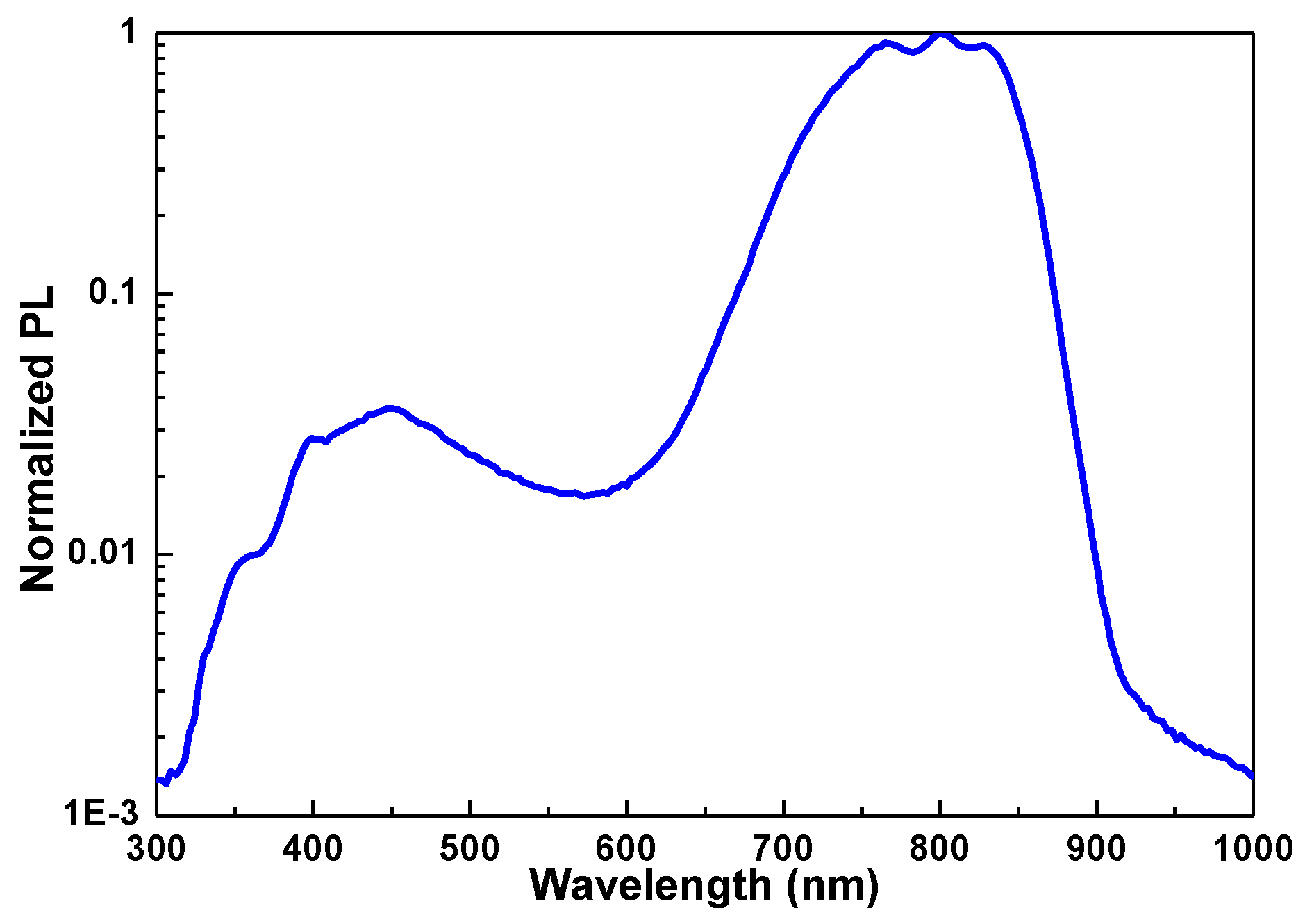
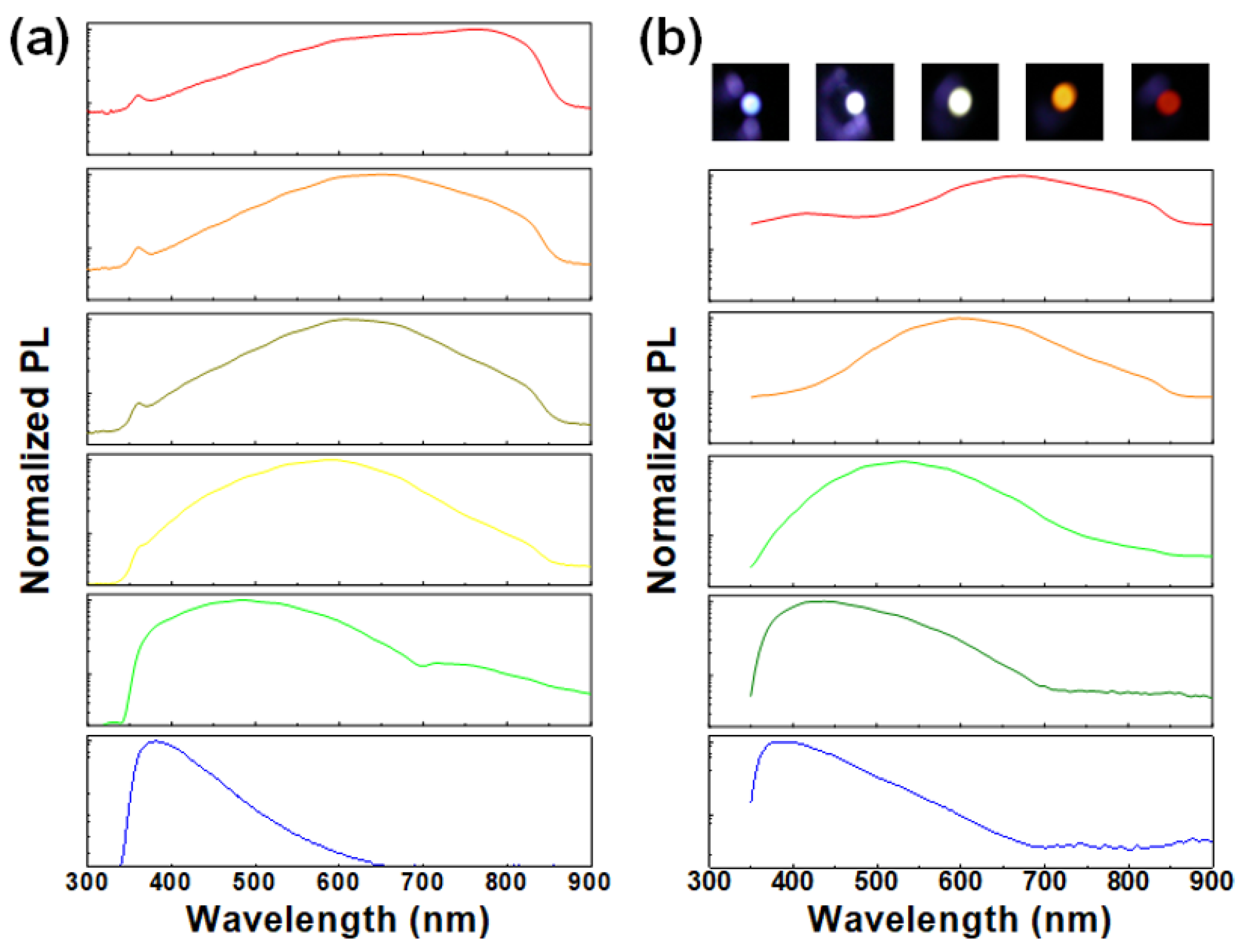
In addition to Si-ion implantation, other methods including sputtering [46,47,48,49,50], e-beam evaporation [51,52], and plasma-enhanced chemical vapor deposition (PECVD) [53,54,55,56,57,58,59,60,61,62] are employed to grow the Si-QDs in host matrix. In 2004, Wu et al. utilized the radio frequency (RF) magnetron sputtering to synthesize Si-QDs in SiO2 matrix with 2–4 nm size for 533–716 nm PL after post-annealing at 600 °C [46]. In particular, Samanta et al. fabricated the SiOx nanowire with buried Si-QDs by using the DC sputtering. The observed PL peak can be blue-shifted from 669 to 575 nm owing to the spatially confinement of Si-QDs within SiOx nanowire [47]. In 2009, Hao et al. further grew the Si-QD/SiO2 multilayer film via the RF sputtering for sandwiching the Si-QDs with SiO2 matrix to provide the red PL emission with a peak wavelength of 800 nm [48]. Moreover, the microcrystalline Si was synthesized in SiOx film via the e-beam evaporation and post-annealing in N2 and O2 gaseous mixture [51]. Similar process was performed by using the thermal evaporation for amorphous SiOx film deposition and post annealing at 1000 °C for Si-QD formation. The buried Si-QDs with an average size of 4.3 nm were formed to generate the broadband red PL emission between 754 and 882 nm [52]. In comparison with sputtering and evaporation, the PECVD method can perform the precise synthesis for the composition ratio variation by adjusting various parameters such as substrate temperature, reactant fluence, RF plasma power, etc. Such a parametric tool facilitates to flexibly grow the buried Si-QDs with precisely controlled sizes in any host matrix. For example, Iacona et al. varied the N2O/SiH4 fluence ratio in PECVD from 6 to 10 to synthesize the SiOx film with different composition ratio [53]. With 1100 °C annealing for Si-QD precipitation, the PL peak is observed to blue-shift from 900 to 650 nm [53]. Alternative approach was proposed by changing the thickness of Si layer during the deposition of Si/SiO2 superlattice. The Si-QD size can be enlarged from 0.9 nm to 2.3 nm for red-shifting the PL peak from 800 to 910 nm [54]. Similarly, the thickness of SiOxNy layer in SiOxNy/SiO2 film can be adjusted for controlling the Si-QD size from 2.5 to 7 nm and red-shifting the PL peak from 729 to 886 nm [55]. Later on, the N2O/SiH4 fluence ratio was varied from 6.8 to 2.3 during the SiOx growth to control its composition ratio. This can effectively reduce Si-QD size in SiOx film with enlarging the O/Si composition ratio such that the less Si content can hardly generate the larger Si-QD in SiOx film [56]. This method helps to enhance the quantum confinement for improving the blue-shift of PL spectrum. With increasing the O/Si composition ratio, a huge PL blue-shift of the buried Si-QD is obtained from 760 to 380 nm [56]. On the contrary, the RF plasma power during the PECVD growth for the Si-QD in SiOx film can be enlarged from 20 W to 70 W to shrink the Si-QD size from 4.5 to 1.7 nm [57]. In our work, Figure 3a exhibits that the PL peak of the buried Si-QDs can be detuned from 800 to 380 nm by adjusting the fabricating parameters during growth.
In contrast to SiOx, either SiNx or SiCx is also considered as host matrix to confine the Si-QDs [63,64,65,66,67,68,69,70,71,72,73,74,75,76]. In 1992, Chen et al. utilized the PECVD and Ar+-laser annealing to fabricate the Si:H/SiNx:H multiple quantum well (MQW). This MQW structure effectively suppresses a full width at half-maximum (FWHM) of PL to only 5 nm [63]. Another approach varied the flow rates of SiH4 and N2 gas to detune the Si-QD size [64]. Reducing the Si-QD size from 6.1 to 2.7 nm significantly blue-shifts the visible PL peak from 850 to 410 nm [64]. Negro et al. used the PECVD method and post-annealed at 700 °C for 60 min to form the Si-QDs in Si-rich SiNx with corresponding PL at 850 nm [65]. In our work, the flexible control on N/Si composition ratio and Si-QD size is demonstrated via the adjustment of NH3 fluence during PECVD synthesis. With increasing the NH3 fluence from 170 to 250 sccm to vary the N/Si composition ratio from 0.85 to 1.32, the observed PL peaks can be blue-shifted from 675 to 385 nm, as shown in Figure 3b. By using the SiC matrix and changing the Si-QD layer thickness in Si-QD/a-SiC superlattice, the Si-QD can shrink its size from 10 to 3 nm for emitting the PL from 1170 to 775 nm [70]. Coscia et al. synthesized the buried Si-QDs in a-SiC via changing the RF plasma power to generate the 636–827 nm PL [71]. Huang et al. changed the SiH4 fluence from 0.5 to 8 sccm to suppress the C/Si composition ratio and increase the Si-QD size for blue-to-green shifting PL wavelength from 440 to 520 nm [72]. Tai et al. further demonstrated the Si-rich SiC synthesis for obtaining red PL between 630 and 660 nm from Si-QDs and 480 nm for SiC-QDs [73,74].
Instead of the Si-QD related PL, the radiative-defect related weak PL by the contribution of structural or interfacial defects in SiOx or SiNx host matrices is comprehensively investigated to realize their bonding mechanisms. Particularly, these defect-related PL emissions are usually located between green- and blue-light regions. The PL spectra of the weak oxygen bond (WOB, denoted as O-O) and neutral oxygen vacancy (NOV, denoted as O3≡Si-Si≡O3) are ranged between 415 and 455 nm [77,78,79,80,81,82]. As a supporting evidence, Cheang-Wong et al. obtained the visible PL peak at 415 nm in Ir2+-doped silica glass owing to the contribution of the WOB defect [77]. Lin et al. also observed the PL at the same wavelength from Si+-implanted SiOx film [78]. In addition, similar PL peak was also observed in SiOx/SiNx superlattice [79]. Tohmon et al. claimed that the PL of NOV defects in oxygen-deficient high-purity silica glass at 459 nm [80]. The blue PL for NOV defects not only in the Si-implanted SiO2 film [81] but also in the RF sputtered Si-rich SiOx film was observed at 460 nm [82]. Other than WOB and NOV defects, the precursor of Si-QDs (E’δ, denoted as Si↑Si-Si) and the non-bridging oxygen hole center (HBOHC, denoted as O3≡Si-O●) defects also contribute to the green and yellow PL [83,84,85,86]. The PL of E’δ defect in the Si-implanted SiOx film without annealing was observed at 653 nm by Shimizu-Iwayama et al. in 1994 [83]. Sakurai et al. analyzed another green PL of the E’δ in oxygen-deficient silica glass at 554 nm [84]. On the other hand, Skuja measured the 653-nm PL of HBOHC defects in silica glass under different temperature condition [85]. For confirmation, Song et al. also reported the PL around 630 nm for the HBOHC defects in Si-implanted SiOx film [86]. In addition to the SiOx host matrix, there are some other defects with radiative recombination in SiNx host matrix [87,88,89]. For example, the PL of Si dangling bonds (denoted as K0 center) is located in the middle of bandgap [87]. In addition, the N4+ center is located close to the conduction band and the N20 center state is close to the valence band [88]. Notably, the PL emission of these K0, N4+, and N20 centers is dependent on the varied optical bandgap of SiNx host matrix by detuning the composition ratio of SiNx film [89]. However, most of their luminescence can be vanished after the annealing recrystallization.
3. Porous Si LED
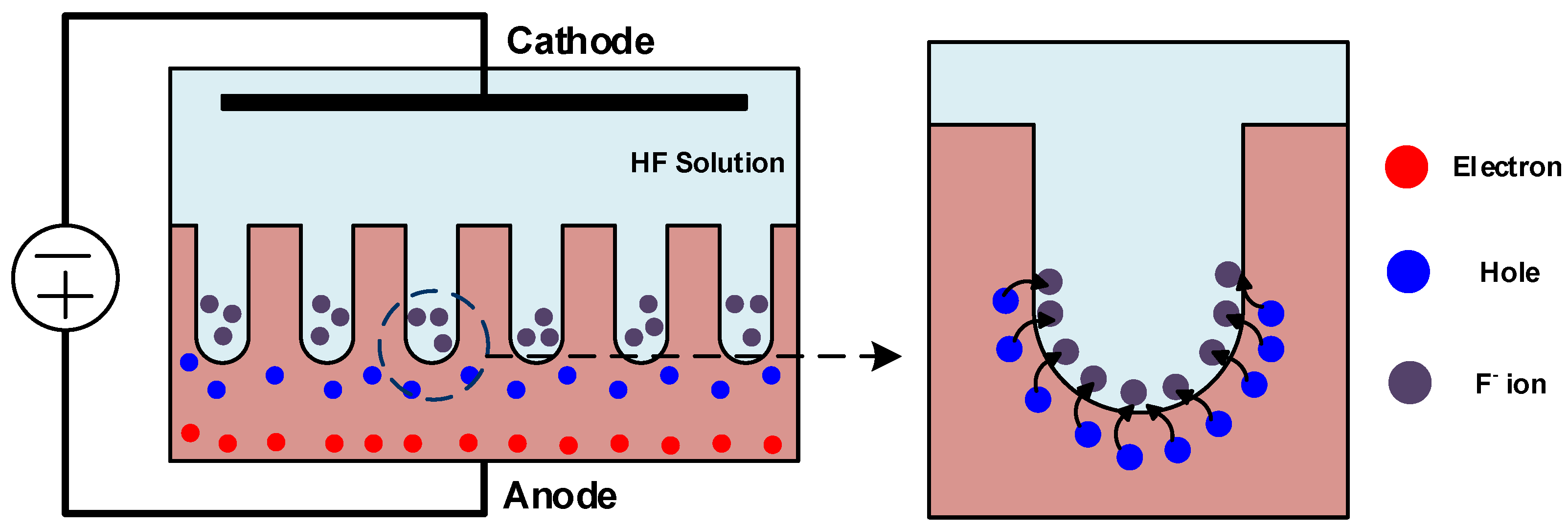
In early years, the fabrication of the Si-QD LED mainly relies on the development status of the porous Si substrate. With using the anodic electrochemical etching process shown in Figure 4, the hydrofluoric acid (HF) at the anode reacts with the crystalline Si to form the porous Si. The porous or island Si structure is generated upon the surface and the Si pillar structure is formed at the flank during the anodic electrochemical etching. Such an etching procedure etches down the Si wafer along direction of its crystalline axis without causing the variation on other directions. However, the doped Si film such as the p-type Si with more holes can somewhat affect the etching process. Gardelis et al. used the anodic electrochemical etching to fabricate the p-type porous Si with a corresponding PL of 709 nm [90]. Dimova-Malinovska et al. found the short-wavelength PL peak of same p-type porous Si at 690 nm [91]. Because of the n-type Si with more electrons, the etching without assistance of illumination or bias can increase more holes to accelerate the etching process. In 1990, Lehmann and Föll utilized tungsten lamping for the enhanced etching formation of porous Si [92]. Theunissen also confirmed that the n-type Si with >1018 cm−3 donor concentration can suffer from the anodic dissolution for hole generation below 10-V bias operation [93]. On the other hand, the porous-like Si nanostructure can also be obtained via a metal-assisted chemical etching method alternatively. Under the interaction with single or double phonons, such Si nanostructure reveals a redshifted and broadened Raman scattering peak when comparing with bulk Si, which is in good agreement with the prediction of phonon confinement effect within Si nanostructure [94].
Moreover, the porous Si diameter can be tunable to vary its PL peaks from 770 to 730 nm by changing the HF concentration [95]. With the tungsten lamp illumination to enhance the reaction rate, the porous Si diameter is gradually shrunk to blue-shift its PL from 709 to 310 nm [35]. A similar etching method was utilized to demonstrate the porous Si with its PL at 479 nm, internal quantum efficiency of 0.1%, and a PL decay time of 1 ns [39]. Prokes et al. increased the etching time to 4 h to decrease the porous Si diameter. This phenomenon also contributes to its PL blue-shifting to 697 nm [38]. With the electrochemical etching with a current density of 50 mA/cm2 for 10 min, the 10-nm QDs can be observed in porous Si with a pore diameter of 3.5 μm and a pore depth of 60 μm to generate the PL at 750 nm [96]. Such simple fabrication for the porous Si urges a rapid development of the porous Si LED in 1990s. The first porous Si LED grown on n-type Si wafer by using anode electrochemical etching with halogen lamp illumination can emit visible luminescence at 650 nm under biasing at 5 mA and 200 V [97]. By lengthening the anode oxidation time from 1 to 7 s, the porous Si LED with a film thickness of 1–2 μm blue-shifted its EL wavelength blue-shifted from 830 to 700 nm [98]. With the fabrication of indium-tin-oxide (ITO)/porous Si/p-Si/aluminum (Al) LED, the EL at 680 nm with external quantum efficiency (EQE) below 10−5% was observed under bias current density of 370 mA/cm2 [99]. Apparently, Canham et al. reached a significant progress on the efficient porous Si LED with its EL peak from 740 to 670 nm via increasing the bias from −1.01 to −1.23 V for the maximal EL density of up to 0.1 W/cm2 [100]. More important, the respectively maximal PL and EL power conversion efficiencies of 1% and 0.1% were ranked top record then [100]. Later on, Koshida and co-workers changed the contact of porous Si LED to the electropolymerized contact for improving the EL intensity. The porous Si LED exhibited its EL peak at 593 nm with the intensity 2.6 times larger than that using Au contact [101]. Steiner et al. were the first group employing the porous p–n junction structure to enhance the EQE of porous Si LED [102]. With the mesoporous p+-Si/nanoporous n-Si/macroporous n-Si structure, the EQE can be effectively improved to 0.01% [102]. In addition, the green and blue EL of porous Si LED at 560 nm and 480 nm was also demonstrated in the same time [103]. Subsequently, Li et al. utilized the conducting polymer contact to replace the Au or ITO contact for improving the EL intensity because it provides relatively higher transparency at emission wavelength of porous Si (630 nm) than Au or ITO [104]. The enhancing EQE of 0.16% from the p+–n–n+-junction-structured porous Si LED with a corresponding EL peak at 630 nm under a pulsed bias of 20 V was reported by Linnors and co-workers in 1995 [105]. In the same year, Loni et al. also demonstrated the visible EL with its EQE of 0.1% under continuous-wave (CW) operation at 2.3 V and 0.01 A/m2 [106]. In 1998, Nishimura et al. further constructed the porous Si LED with a p+-n structure to enhance its EQE to 0.8% [107]. With using the semitransparent Au as electrode, the EQE of device can be expected to exceed 1% [107]
In view of previous reports, the porous Si can be regarded as the active layer, however, the porous Si is easily oxidized to degrade its EL stability as the extremely large porous Si surface reacts with abundant oxygen molecules [108,109,110,111,112]. In 1996, Tsybeskov et al. passivated the porous Si surface by annealing the layer at 800–900 °C to extend the LED stability without suffering from power degradation during pulsed operation over one month [108]. Another method employed thin transparent alumina layer to protect the porous Si surface for achieving the CW operation over one month [109]. Alternative approach via the anodic oxidation to oxidize the porous Si surface has also emerged to effectively enhance the EQE to 0.21% and extend its operation time to 8 min with an intensity decay of <10% [110]. A similar approach employed the electrochemically oxidizing thin porous Si layer to enhance the EQE over 1% with intensity degradation by only 8% within 120 s [111]. Other works on the surface passivation of porous Si layer were demonstrated via the covalent bonding with organic monolayers. This method maintains the unchanged EL intensity of porous Si LED during 2-h operation [112]. In 2006, the high-pressure water vapor annealing technology was also developed to maintain the EL intensity without decay during 20-min operation [113]. Even though tremendous efforts were paid to improve the device stability, its EQE is still too low to enable its practical application.
4. Si-Implanted Si-QD LEDs
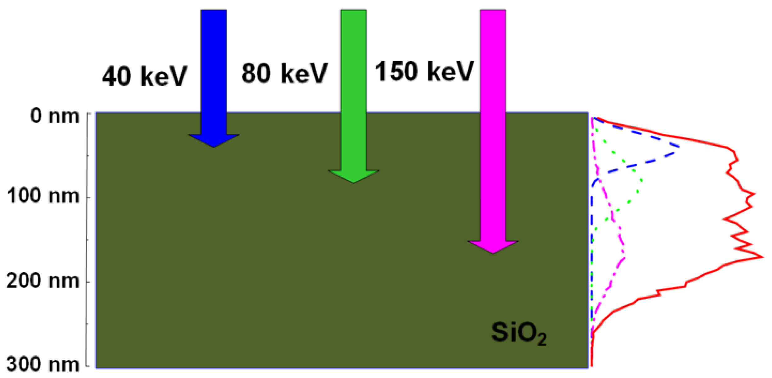
To take over porous Si LED with instable and low EQE during long-term operation, the Si-ion implantation into SiO2 or Si3N4 host matrix for the Si-QD formation has emerged in the beginning of 21st century. This method self-aggregates these excessive Si+ ions as Si-QDs with their sizes tuning by changing the dose concentration of Si+ ions. At beginning, Shimizu-Iwayama and co-workers varied the dose concentration from 1 × 10¹⁷ to 4 × 10¹⁷ ions/cm2 for Si-implanted SiOx synthesis. With increasing dose concentration of Si+ ions to enlarge the Si-QD size in SiOx film, the red-shifted luminescent variation was observed under room-temperature operation [83]. Unfortunately, the implanted Si+ ions only distribute in a very shallow layer beneath the surface of host matrix. For example, the Si+-ions with dose concentration of 5 × 10¹⁶ ions/cm2 and energy of 40 keV can only cover a depth of 60 nm from the SiO2 surface with non-uniform distribution of implantation ions according to the transportation of ions in matter (TRIM) software simulation [114]. Such shallow and non-uniform distribution can be overcome through multiple ion-implantation with different dose concentrations and energies. This method can approach the depth of 350 nm with employing different implantation energies at same Si dose concentration of 1016 ions/cm2 [115]. By taking one example in detail, the implanted dose recipes of Si+ ions were set as 5 × 10¹⁵ ions/cm2 at 40 keV, 1 × 10¹⁶ ions/cm2 at 80 keV, and 2.5 × 10¹⁶ ions/cm2 at 150 keV to uniformly distribute the excessive Si atoms in SiOx layer with its depth between 10 and 200 nm from the surface [116]. As shown in Figure 5, using the lower (higher) dose concentration and smaller (larger) implantation energy makes the Si+ ions stay with shallower (deeper) depth from SiO2 surface with narrower (broader) distribution. With post-annealing the Si-implanted SiOx for aggregating the Si-QDs, recrystallizing the host matrix and suppressing the structural defects in host matrix, numerous studies of the Si-implanted Si-QD LED have been reported [117,118,119,120,121,122,123,124,125,126,127].
In 1996, the Si-implanted Si-QD in SiO2 layer with a thickness of 300 nm was synthesized by using a recipe with Si+-ion dose concentration of 2 × 10¹⁶ ions/cm2 and implantation energy of 120 keV to perform EL at 620 nm under a bias at 15 V [117]. A latter experiment used 200-keV Si+-ions with dose concentration of 3 × 10¹⁶ ions/cm2 as first recipe and 100-keV Si+-ions with 1.8 × 10¹⁶ ions/cm2 as the second recipe to increase the excessive Si content in SiO2 film. Then, the fabricated Si-QD LED performed its EL at 455 nm under a bias with current of 100 nA and voltage of 370 V [118]. In contrast, Song and co-workers utilized Si+-ions implantation at 25 keV with dose concentration of 1 × 10¹⁶ ions/cm2 and post-annealed the Si-implanted SiO2 film with temperature increasing from 100 °C to 1100 °C [119]. The LED exhibited the enhancement on the Si-QD-related EL peak at 730 nm and the degradation on the defect-related EL peaks at 470 and 600 nm. With raising the Si+ dose concentration from 3 × 10¹⁶ to 3 × 10¹⁷ ions/cm2 under constant implantation energy of 150 keV to enlarge the Si-implanted SiO2 thicknesses from 12 to 18 nm, the Si-implanted Si-QD LED red-shifts its EL peak from 752 to 855 nm under a bias voltage of 16 V, and shortens its EL decay time from 100 to 6 μs [120]. In 2005, Walters and co-workers employed the Si-implanted Si-QDs in SiOx layer as the active layer to implement the metal-oxide-semiconductor LED (MOSLED). This device contains the Si-QDs with average size of 2–4 nm to demonstrate EL emission at 750 nm with a decay time of 2.5 μs under a bias voltage of 6 V [121]. In addition, our work employs the multiple ion-implantation and post annealing to demonstrate the Si-QD dependent EL from Si-implanted SiOx LED. Figure 6 reveals the EL between 400 and 600 nm with the blue emission by the WOB and NOV defects (405–455 nm), green emission via the precursor of Si-QDs (520 nm), and red emission from the larger Si-QDs (600 nm), as shown in Figure 6. The turn-on current and voltage are respectively measured as only 0.2 mA and 5 V, as shown in the inset of Figure 6. The maximal power achieves 100 nW under biasing at 10 V and 70 mA.
Besides, the Si3N4 host matrix is also employed to fabricate the Si-implanted Si-QDs in SiNx film [124,125,126,127]. In 2009, Cen et al. utilized the multiple ion-implantation with the Si+ dose concentrations of 4 × 10¹⁶ ions/cm2 at 25 keV at the first time, 8 × 10¹⁵ ions/cm2 at 8 keV at the second time, and 3 × 10¹⁵ ions/cm2 at 2 keV at the third time into Si3N4 film to form the Si-implanted Si-QD in SiNx film with an average excess Si concentration of 1.2 × 1022 cm−3 [124]. This LED exhibits three main EL peaks at 886 nm, 564 nm, and 413 nm [124]. The EL peak at 886 nm is attributed to the Si-QDs and other two EL peaks at 564 and 413 nm are contributed by the structural defects [124]. With the Si+ dose concentration enlarging from 2 × 10¹⁶ ions/cm2 to 4 × 10¹⁶ ions/cm2, the excessive Si content in SiNx film also increases to form more Si-QDs. This Si-implanted Si-QD LED exhibits its green-yellow EL and the promoting EQE of 10−4–10−3% [125,126,127]. Nevertheless, most of the previous reports for the Si-implanted Si-QD LEDs seldom mentioned their EQE as the uniform size distribution of Si-QDs in host matrix is still hardly achieved for providing efficient visible luminescence. In addition, the structural damage in SiOx or SiNx film is too serious such that a lot of irradiative defects appear to scatter or absorb electron-hole pairs for efficient recombination. Therefore, the PECVD-grown Si-QD LED with less damaged structure than the implanted device gradually develops as the main-stream device nowadays.
5. PECVD Grown Si-QD LED
In the 2000s, the PECVD-grown Si-QD LED has emerged not only because of its reduced structural imperfection but also because of its precise control on the Si-QD size distribution. In addition, the PECVD-grown Si-QDs can more uniformly exist in host matrix as compared to other syntheses. For example, the transmission electron microscopy (TEM) image of the PECVD-grown Si-QDs in Si-rich SiOx film is shown in the upper part of Figure 7. From the upper part of Figure 7, the thickness of Si-rich SiOx layer can be evaluated as 200 nm. To observe the Si-QDs in Si-rich SiOx, the high-resolution TEM (HR-TEM) image of the Si-QDs in Si-rich SiOx film is shown in the lower part of Figure 7. The Si-QDs with their size between 2.4 and 5.6 nm are observed and the Si-QD volume density is estimated as 1.1 × 1018 cm−3. Versatile orientations of Si-QDs in Si-rich SiOx film are evaluated as (110), (111), (002), and (021) with the corresponding plane spaces of 0.38, 0.31, 0.27, and 0.24 nm, respectively. In comparison with porous Si and implanted Si-QDs, the density and size of PECVD-grown Si-QDs can easily be controlled by varying the reactant gas content, the substrate temperature, and the RF plasma power during growth. As a result, the PECVD becomes the most common technology for the Si-QD synthesis [128,129,130,131,132,133,134,135,136,137,138,139,140,141,142,143]. In 2002, Franzò et al. employed SiH4 and N2O molecules as reactant gaseous for the growth of the Si-rich SiOx sample, and performed the post-annealing at 1100–1250 °C to form the Si-QDs [130]. For the Si concentration of 46% in Si-rich SiOx film, the EL peak of SiOx MOSLED with buried 1-nm Si-QDs can be observed at 850 nm under biasing at 50 V and 0.2 A/cm2 [130]. In addition, the SiOx MOSLED with average Si-QD size of 4 nm exhibited its EL peaks at 700 nm and maximal output power of 48 nW with a corresponding P–I slope of 0.84 mW/A under a bias at 86 V [130]. The EQE can be also obtained as 1.6 × 10⁻³% [131]. The Si nanopyramids were also used at SiOx/Si interface for decreasing the turn-on voltage and increasing the turn-on current density to enhance the current injection and recombination efficiency. This method significantly enhanced its EL power to 30 nW and maintained the EL intensity over 10 h [132,133]. In 2006, Perálvarez et al. fabricated the Si-QDs with an average size of 3.6 nm and a volume density of 5 × 1017 cm−3 in Si-rich SiOx film as luminescent centers to achieve its EL peak at 816 nm, EL decay lifetime of 5 μs, and EQE of 0.03% [134].
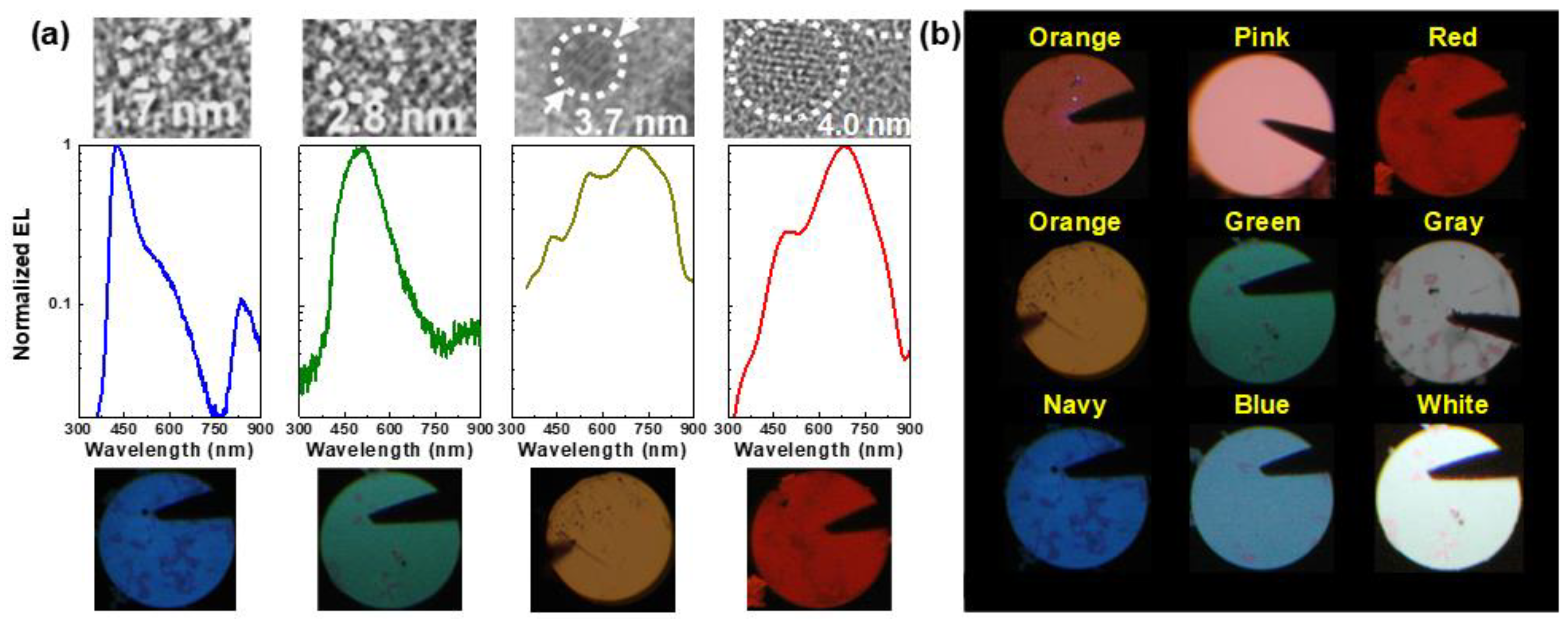
Similar material was employed to demonstrate the Si-QD MOSLED with two main EL wavelengths of 740 and 1000 nm [135]. In 2007, Barreto et al. also constructed the 815-nm Si-QD MOSLED with its turn-on voltage of 15 V and EQE of 0.03% [136]. Lin et al. also utilized the CO2 laser annealing to generate the Si-QDs in SiOx MOSLED [137]. Three main EL peaks at 590, 715, and 810 nm are contributed by different-size Si-QDs to achieve the maximal output of 50 nW under a bias at 85 V and 2.3 mA/cm2 [137]. The Si nanopillars with a size of 30 nm, a height of 350 nm, and an area density of 2.8 × 1010 cm−2 were employed in Si-QD MOSLED to enhance the current injection. This device obtained its maximal output power of 700 nW with a corresponding P–I slope of 2.8 ± 0.8 mW/A to achieve the EQE of 0.1% under biasing at 0.375 mA [138]. In 2008, Chen and co-workers employed the Si-QD/SiO2 multilayers to enhance the EL intensity of the Si-QD p-i-n LED by 50 times than single-layered Si-QD LED [139]. In 2009, Anopchenko et al. further used the SiO2/Si-QD in SiOx multilayers to demonstrate the power efficiency of 0.01% for Si-QD MOSLED under 1-μA bias operation [140]. With increasing the bias voltage from 2.5 to 6 V, the EL peak can be blue-shifted from 916 to 827 nm [140]. Moreover, the EL peak of MOSLED can be blue-shifted from 700 to 430 nm by suppressing the average Si-QD size from 4 to 1.7 nm to achieve the maximal output power of 1 μW and the EQE of 2.4% [141,142,143]. In our work, decreasing the Si-QD size can effectively blue-shift the EL peak with a corresponding EL pattern from red to blue, as shown in Figure 8a. Therefore, adjusting the fabricating parameters to detune the Si-QD size demonstrates versatile-color Si-QD MOSLED, as shown in Figure 8b.
In recent years, the SiNx dielectric material becomes another host matrix to demonstrate the Si-QD LED although the SiNx material has the lower energy bandgap to degrade the quantum confinement effect [144,145,146,147,148,149,150,151,152]. In 2001, Park and co-workers fabricated the Si-QDs in SiNx to exhibit its EL peak at 620 nm and turn-on voltage of <5 V, and the EQE of 2 × 10⁻³% [144]. In 2005, Cho et al. used the SiH4 and NH3 molecules as reactant gaseous to fabricate the Si-QDs in Si-rich SiNx film. The Si-QD LED obtained its EL at 600 nm, maximal output power of 2.3 mW, and maximal EQE to 1.6% under biasing at 70 mA [145]. The periodic micron-scale rugged SiNx patterns were fabricated on the surface of Si-QD LED to increase the light extraction efficiency by 2.8 time than the flat-surfaced Si-QD LED [146]. In addition, the Ni/Au contact was also used to enhance the carrier injection for improving EQE by 10−65% as compared to the amorphous Si-QD LED [147]. Huh et al. further utilized the 2.5-nm-thick Ag interlayer inserting between the indium tin oxide (ITO) contact layer and SiC doping layer to enlarge the output power by 40% [148]. Moreover, the undoped SiC layer was added between the Si-QD active layer and n-type SiC layer to enhance the output power [149]. In 2010, Lin et al. compared the lighting performance of SiNx and SiOx LED [150]. Owing to the lower barriers at Si-QD/SiNx and Al/SiNx interfaces, the SiNx LED has a lower turn-on voltage of 10.45 V to easily escape the electrons and holes from Si-QD to decrease the EQE [150,151].
In our work, the Si-QD LED exhibits its EL peak at 740 nm because of the contribution of Si-QDs, as shown in Figure 9. In addition, the EL peak at 420 nm is attributed to the structural defects in SiNx host matrix. In 2012, Huang et al. also fabricated the Si-QDs with an average size of 2.4 nm and an area density of 4.6 × 1012 cm−2 in Si-rich SiNx film to demonstrate the 710-nm Si-QD LED [152]. Owing to the dielectric host matrix with the relatively large resistivity to decrease the current injection efficiency, the SiC semiconductor was selected as a candidate of host matrices [153,154,155,156,157]. In 2011, Rui et al. detuned the Si-QD from 4.2 to 1.4 nm in SiC host matrix by detuning the C/Si composition ratio and annealing temperature to blue-shift the EL peak of the Si-QD LED from 775 to 539 nm. Moreover, the 2.7-nm Si-QDs in Si-QD/SiC multilayer were used as active layer. This Si-QD LED exhibited its EL peak at 650 nm and improved EL power by 8.6 times than the device with the Si-QD/SiC single layer [154]. Wang and co-workers also fabricated the SiC LED with a p-i-n structure to observe two EL peaks at 689 and 775 nm owing to the contribution of different-size Si-QDs [155]. Cheng et al. changed the substrate temperature from 300 °C to 650 °C during the growth to detune the average Si-QD size from 2.5 to 2.7 nm. This method respectively decreased the turn-on voltage and current of yellow-light Si-QD LED to 4.2 V and 0.42 mA to enhance the maximal output power density to 8.52 μW/cm2 with a corresponding P–I curve of 0.75 μW/A [156]. Tai and co-workers further suppressed the thickness of SiC with buried Si-QDs to 50 nm to enhance the EQE to 0.158% [157]. In our work, Figure 10 exhibits the EL peaks at 480, 700, and 850 nm for Si-QD LED owing to the contribution of the different-size Si-QD. From abovementioned works, the performance of Si-QD LED can be improved.
Up until now, the Si-QD LEDs via versatile syntheses are still developed and studied for visible light emission but also for color conversion and optical switching applications in the future. On the basis of abovementioned works, the studies of Si-QD LED approaches more piratical application in recent three years. In 2018, Hsu et al. inserted Si-QDs into Al2O3 membrane to confine the size distribution. The confined size distribution can suppress the luminescent linewidth [158]. In addition, Zhao et al. utilized the Al2O3 material as interlayer to suppress the exciton quenching and hole accumulation and reduce the carrier leakage [159]. This interlayer effectively improved the optical density and EQE of Si-QD LED to 14 μW/cm2 and 0.1%. In 2018, Ghosh et al. firstly demonstrated the flexible red Si-QD LED with its luminance of 5000 cd/m2 and EQE of 3.1% on polyethylene terephthalate substrate [160]. In 2019, the same group used ITO/ZnO/Si-QD/WO3/Al multilayer to construct the red Si-QD LED with its EQE of 0.25% and luminance of 1400 cd/m2 [161]. This device without any encapsulation can maintain its EL performance under 80% humidity in ambient air over 45 days [161]. In 2020, Zhang further demonstrated the white-light Si-QD LED to provide a possibility to replace the commercial LED in the future [162]. This device exhibited its luminance of 225.8 cd/m2 and EQE of 1% under biasing at 2.9 V [162].
6. Conclusions
In view of previous progress on the Si-QD based electronics and photonics, various syntheses have been developed to enable versatile applications of the Si-QDs for light emission, color conversion and switching. For efficient visible light emission, the EL emission wavelength of Si-QD LEDs has been demonstrated to be widely tunable from 400 to 1000 nm with corresponding EQE varied from 0.1–2% obtained by optimizing the selected material synthesis and device design for implementing visible and near-infrared LEDs. In addition, the real EL power of Si-QD LEDs was observed between 30 nW and 2.3 mW. However, different syntheses such as porous Si etching, Si-ion implantation, and excessive Si deposition also reveal their inherent limitations and individually contribute to some weakness for developing the Si-QD LED with sufficient EQE and power. Up until now, versatile studies specially on improving the conductive host matrix, transparent contact electrode, and spatially-confined synthesis are still going to enhance the stability and efficiency of the Si-QD LED. For different market demands, the fabricated Si-QD by mature syntheses has been comprehensively utilized not only for visible light emission but also for color conversion and optical switching applications in future academic and industrial applications.
Author Contributions
Conceptualization, C.-H.C. and G.-R.L.; Methodology, C.-H.C. and G.-R.L.; Data curation, C.-H.C. and G.-R.L.; Writing—original draft preparation, C.-H.C. and G.-R.L.; Writing-review and editing, C.-H.C. and G.-R.L. All authors have read and agreed to the published version of the manuscript.
Funding
This research was funded by Ministry of Science and Technology, Taiwan, grant number MOST 106-2221-E-002-152-MY3, MOST 107-2221-E-002-159-MY3, MOST 107-2221-E-002-158-MY3, MOST 107-2218-E-992-304-, and MOST 108-2218-E-992-302-.
Acknowledgments
The authors thank Ministry of Science and Technology, Taiwan, R.O.C. for the support granted by the MOST 106-2221-E-002-152-MY3, MOST 107-2221-E-002-159-MY3, MOST 107-2221-E-002-158-MY3, MOST 107-2218-E-992-304-, and MOST 108-2218-E-992-302-.
Conflicts of Interest
The authors declare no conflict of interest.
References
- Streeman, B.G.; Banerjee, S. Solid State Electronic Devices, 5th ed.; Prentice Hall: Upper Saddle River, NJ, USA, 2000; p. 524. [Google Scholar]
- Macfarlane, G.G.; McLean, T.P.; Quarrington, J.E.; Roberts, V. Exciton and phonon effects in the absorption spectra of germanium and silicon. J. Phys. Chem. Solids 1959, 8, 388–392. [Google Scholar] [CrossRef]
- Namazu, T.; Isono, Y.; Tanaka, T. Evaluation of size effect on mechanical properties of single crystal silicon by nanoscale bending test using AFM. J. Microelectromech. Syst. 2000, 9, 450–459. [Google Scholar] [CrossRef]
- Onida, O.; Andreoni, W. Effect of size and geometry on the electronic properties of small hydrogenated silicon clusters. Chem. Phys. Lett. 1995, 243, 183–189. [Google Scholar] [CrossRef]
- Furukawa, S.; Miyasato, T. Quantum size effects on the optical band gap of microcrystalline Si:H. Phys. Rev. B 1988, 38, 5726–5729. [Google Scholar] [CrossRef] [PubMed]
- Canham, L.T. Silicon quantum wire array fabrication by electrochemical and chemical dissolution of wafers. Appl. Phys. Lett. 1990, 57, 1046–1048. [Google Scholar] [CrossRef]
- Barbagiovanni, E.G.; Lockwood, D.J.; Simpson, P.J.; Goncharova, L.V. Quantum confinement in Si and Ge nanostructures. J. Appl. Phys. 2012, 111, 034307. [Google Scholar] [CrossRef] [Green Version]
- Yang, J.; Ono, T.; Esashi, M. Surface effects and high quality factors in ultrathin single-crystal silicon cantilevers. Appl. Phys. Lett. 2000, 77, 3860–3862. [Google Scholar] [CrossRef] [Green Version]
- Lehmann, V.; Hofmann, F.; Möller, F.; Grüning, U. Resistivity of porous silicon: A surface effect. Thin Solid Films 1995, 255, 20–22. [Google Scholar] [CrossRef]
- Goldstein, A.N. The melting of silicon nanocrystals: Submicron thin-film structures derived from nanocrystal precursors. Appl. Phys. A 1996, 62, 33–37. [Google Scholar] [CrossRef]
- Cao, Y.Q.; Lu, P.; Zhang, X.W.; Xu, J.; Xu, L.; Chen, K.J. Enhanced photovoltaic property by forming p-i-n structures containing Si quantum dots/SiC multilayers. Nanoscale Res. Lett. 2014, 9, 634. [Google Scholar] [CrossRef] [Green Version]
- Askari, S.; Haq, A.U.; Macias-Montero, M.; Levchenko, I.; Yu, F.J.; Zhou, W.Z.; Ostrikov, K.; Maguire, P.; Svrcekg, V.; Mariotti, D. Ultra-small photoluminescent silicon-carbide nanocrystals by atmospheric-pressure plasmas. Nanoscale 2016, 8, 17141–17149. [Google Scholar] [CrossRef] [PubMed] [Green Version]
- Meier, C.; Gondorf, A.; Lüttjohann, S.; Lorke, A. Silicon nanoparticles: Absorption, emission, and the nature of the electronic bandgap. J. Appl. Phys. 2007, 101, 103102. [Google Scholar] [CrossRef]
- Meier, C.; Lüttjohann, S.; Offer, M.; Wiggers, H.; Lorke, A. Silicon nanoparticles: Excitonic fine structure and oscillator strength. In Advances in Solid State Physics, 1st ed.; Haug, R., Ed.; Springer: New York, NY, USA, 2009; Volume 48, pp. 79–90. [Google Scholar]
- Xia, J.-B. Electronic structures of zero-dimensional quantum wells. Phys. Rev. B 1989, 40, 8500–8507. [Google Scholar] [CrossRef] [PubMed]
- Yoffe, A.D. Low-dimensional systems: Quantum size effects and electronic properties of semiconductor microcrystallites (zero-dimensional systems) and some quasi-two-dimensional systems. Adv. Phys. 2002, 51, 799–890. [Google Scholar]
- Kanemitsu, Y.; Uto, H.; Masumoto, Y.; Matsumoto, T.; Futagi, T.; Mimura, H. Microstructure and optical properties of free-standing porous silicon films: Size dependence of absorption spectra in Si nanometer-sized crystallites. Phys. Rev. B 1993, 48, 2827–2830. [Google Scholar] [CrossRef] [PubMed] [Green Version]
- Takagi, H.; Ogawa, H.; Yamazaki, Y.; Ishizaki, A.; Nakagiri, T. Quantum size effects on photoluminescence in ultratfne Si particles. Appl. Phys. Lett. 1990, 56, 2379–2380. [Google Scholar] [CrossRef]
- Maeda, Y.; Tsukamoto, N.; Yazawa, Y.; Kanemitsu, Y.; Masumoto, Y. Visible photoluminescence of Ge microcrystals embedded in SiO2 glassy matrices. Appl. Phys. Lett. 1991, 59, 3168–3170. [Google Scholar] [CrossRef] [Green Version]
- Matsumoto, T.; Takahashi, J.; Tamaki, T.; Futagi, T.; Mimura, H.; Kanemitsu, Y. Blue-green luminescence from porous silicon carbide. Appl. Phys. Lett. 1994, 26, 226–228. [Google Scholar] [CrossRef]
- DiMaria, D.J.; Kirtley, J.R.; Pakulis, E.J.; Dong, D.W.; Kuan, T.S.; Pesavento, F.L.; Theis, T.N.; Cutro, J.A.; Brorson, S.D. Electroluminescence studies in silicon dioxide films containing tiny silicon islands. J. Appl. Phys. 1984, 56, 401–415. [Google Scholar] [CrossRef]
- Qin, G.G.; Wang, Y.Q.; Qiao, Y.P.; Zhang, B.R.; Ma, Z.C.; Zong, W.H. Synchronized swinging of electroluminescence intensity and peak wavelength with Si layer thickness in Au/SiO2/nanometer Si/SiO2/p-Si structures. Appl. Phys. Lett. 1999, 74, 2182–2184. [Google Scholar] [CrossRef]
- Pavesi, L.; Negro, L.D.; Mazzoleni, C.; Franzò, G.; Priolo, F. Optical gain in silicon nanocrystals. Nature 2000, 408, 440–444. [Google Scholar] [CrossRef] [PubMed]
- Irrera, A.; Pacifici, D.; Miritello, M.; Franzò, G.; Priolo, F. Excitation and de-excitation properties of silicon quantum dots under electrical pumping. Appl. Phys. Lett. 2002, 81, 1866–1868. [Google Scholar] [CrossRef]
- Lin, G.-R.; Lin, C.-J.; Lin, C.-K.; Chou, L.-J.; Chueh, Y.-L. Oxygen defect and Si nanocrystal dependent white-light and near-infrared electroluminescence of Si-implanted and plasma-enhanced chemical-vapor deposition-grown Si-rich SiO2. J. Appl. Phys. 2005, 97, 094306. [Google Scholar] [CrossRef] [Green Version]
- Chen, L.-Y.; Chen, W.-H.; Hong, F.C.-N. Visible electroluminescence from silicon nanocrystals embedded in amorphous silicon nitride matrix. Appl. Phys. Lett. 2005, 86, 193506. [Google Scholar] [CrossRef] [Green Version]
- Wu, C.-L.; Lin, G.-R. Inhomogeneous linewidth broadening and radiative lifetime dispersion of size dependent direct bandgap radiation in Si quantum dot. AIP Adv. 2012, 2, 042162. [Google Scholar] [CrossRef]
- Lin, G.-R.; Lin, C.-J.; Lin, C.-T. Low-plasma and high-temperature PECVD grown silicon-rich SiOx film with enhanced carrier tunneling and light emission. Nanotechnology 2007, 18, 395202. [Google Scholar] [CrossRef]
- Huang, R.; Chen, K.J.; Han, P.G.; Dong, H.P.; Wang, X.; Chen, D.Y.; Li, W.; Xu, J.; Ma, Z.Y.; Huang, X.F. Strong green-yellow electroluminescence from oxidized amorphous silicon nitride light-emitting devices. Appl. Phys. Lett. 2007, 90, 093515. [Google Scholar] [CrossRef]
- Lin, G.-R.; Lin, C.-J.; Kuo, H.-C.; Lin, H.-S.; Kao, C.-C. Anomalous microphotoluminescence of high-aspect-ratio Si nanopillars formatted by dry-etching Si substrate with self-aggregated Ni nanodot mask. Appl. Phys. Lett. 2007, 90, 143102. [Google Scholar] [CrossRef]
- Lin, Y.-H.; Wu, C.-L.; Pai, Y.-H.; Lin, G.-R. A 533-nm self-luminescent Si-rich SiNx/SiOx distributed Bragg reflector. Opt. Express 2011, 19, 6563–6570. [Google Scholar] [CrossRef]
- Bsiesy, A.; Vial, J.C.; Gaspard, F.; Herino, R.; Ligeon, M.; Muller, F.; Romestain, R.; Wasiela, A.; Halimaoui, A.; Bomchil, G. Photoluminescence of high porosity and of electrochemically oxidized porous silicon layers. Surf. Sci. 1991, 254, 195–200. [Google Scholar] [CrossRef]
- Tsai, C.; Li, K.-H.; Sarathy, J.; Shih, S.; Campbell, J.C.; Hance, B.K.; White, J.M. Thermal treatment studies of the photoluminescence intensity of porous silicon. Appl. Phys. Lett. 1991, 59, 2814–2816. [Google Scholar] [CrossRef]
- Koshida, N.; Koyama, H. Efficient visible photoluminescence from porous silicon. Jpn. J. Appl. Phys. 1991, 30, L1221–L1223. [Google Scholar] [CrossRef]
- Mizuno, H.; Koyama, H.; Koshida, N. Oxide-free blue photoluminescence from photochemically etched porous silicon. Appl. Phys. Lett. 1996, 69, 3779–3781. [Google Scholar] [CrossRef]
- Tsu, R.; Shen, H.; Dutta, M. Correlation of Raman and photoluminescence spectra of porous silicon. Appl. Phys. Lett. 1992, 60, 112–114. [Google Scholar] [CrossRef]
- Ben-Chorin, M.; Kux, A.; Schechter, I. Adsorbate effects on photoluminescence and electrical conductivity of porous silicon. Appl. Phys. Lett. 1994, 64, 481–483. [Google Scholar] [CrossRef]
- Prokes, S.M.; Glembocki, O.J.; Bermudez, V.M.; Kaplan, R.; Friedersdorf, L.E.; Searson, P.C. SiHx excitation: An alternate mechanism for porous Si photoluminescence. Phys. Rev. B 1992, 45, 13788–13791. [Google Scholar] [CrossRef]
- Tsybeskov, L.; Vandyshev, J.V.; Fauchet, P.M. Blue emission in porous silicon: Oxygen-related photoluminescence. Phys. Rev. B 1994, 49, 7821–7824. [Google Scholar] [CrossRef]
- Mishra, J.K.; Bhunia, S.; Banerjee, S.; Banerji, P. Photoluminescence studies on porous silicon/polymer heterostructure. J. Lumin. 2008, 128, 1169–1174. [Google Scholar] [CrossRef]
- Mutti, P.; Ghislotti, G.; Bertoni, S.; Bonoldi, L.; Cerofolini, G.F.; Meda, L.; Grilli, E.; Guzzi, M. Room-temperature visible luminescence from silicon nanocrystals in silicon implanted SiO2 layers. Appl. Phys. Lett. 1995, 66, 851–853. [Google Scholar] [CrossRef]
- Min, K.S.; Shcheglov, K.V.; Yang, C.M.; Atwater, H.A.; Brongersma, M.L.; Polman, A. Defect-related versus excitonic visible light emission from ion beam synthesized Si nanocrystals in SiO2. Appl. Phys. Lett. 1996, 69, 2033–2035. [Google Scholar] [CrossRef] [Green Version]
- Shimizu-Iwayama, T.; Kurumado, N.; Hole, D.E.; Townsend, P.D. Optical properties of silicon nanoclusters fabricated by ion implantation. J. Appl. Phys. 1998, 83, 6018–6022. [Google Scholar] [CrossRef]
- Linnros, J.; Lalic, N.; Galeckas, A.; Grivickas, V. Analysis of the stretched exponential photoluminescence decay from nanometersized silicon crystals in SiO2. J. Appl. Phys. 1999, 86, 6128–6134. [Google Scholar] [CrossRef]
- Lin, G.-R.; Lin, C.-J.; Yu, K.-C. Time-resolved photoluminescence and capacitance–voltage analysis of the neutral vacancy defect in silicon implanted on silicon substrate. J. Appl. Phys. 2004, 96, 3025–3027. [Google Scholar] [CrossRef]
- Wu, X.L.; Xue, F.S. Optical transition in discrete levels of Si quantum dots. Appl. Phys. Lett. 2004, 84, 2808–2810. [Google Scholar] [CrossRef]
- Samanta, A.; Das, D. SiOx nanowires with intrinsic nC-Si quantum dots: The enhancement of the optical absorption and photoluminescence. J. Mater. Chem. C 2013, 1, 6623–6629. [Google Scholar] [CrossRef]
- Hao, X.J.; Podhorodecki, A.P.; Shen, Y.S.; Zatryb, G.; Misiewicz, J.; Green, M.A. Effects of Si-rich oxide layer stoichiometry on the structural and optical properties of Si QD/SiO2 multilayer films. Nanotechnology 2009, 20, 485703. [Google Scholar] [CrossRef] [Green Version]
- Di, D.; Perez-Wurfl, I.; Conibeer, G.; Green, M.A. Formation and photoluminescence of Si quantum dots in SiO2/Si3N4 hybrid matrix for all-Si tandem solar cells. Sol. Energy Mater. Sol. Cells 2010, 94, 2238–2243. [Google Scholar] [CrossRef]
- Conibeer, G.; Green, M.; Corkish, R.; Cho, Y.; Cho, E.-C.; Jiang, C.-W.; Fangsuwannarak, T.; Pink, E.; Huang, Y.; Puzzer, T.; et al. Silicon nanostructures for third generation photovoltaic solar cells. Thin Solid Film. 2006, 511–512, 654–662. [Google Scholar] [CrossRef]
- Ye, Q.-Y.; Tsu, R.; Nicollian, E.H. Resonant tunneling via microcrystalline-silicon quantum confinement. Phys. Rev. B 1991, 44, 1806–1811. [Google Scholar] [CrossRef]
- Kahler, U.; Hofmeister, H. Visible light emission from Si nanocrystalline composites via reactive evaporation of SiO. Opt. Mater. 2001, 17, 83–86. [Google Scholar] [CrossRef]
- Iacona, F.; Franzò, G.; Spinella, C. Correlation between luminescence and structural properties of Si nanocrystals. J. Appl. Phys. 2000, 87, 1295–1303. [Google Scholar] [CrossRef]
- Vinciguerra, V.; Franzò, G.; Priolo, F.; Iacona, F.; Spinella, C. Quantum confinement and recombination dynamics in silicon nanocrystals embedded in Si/SiO2 superlattices. J. Appl. Phys. 2000, 87, 8165–8173. [Google Scholar] [CrossRef]
- Hartel, A.M.; Hiller, D.; Gutsch, S.; Löper, P.; Estradé, S.; Peiró, F.; Garrido, B.; Zacharias, M. Formation of size-controlled silicon nanocrystals in plasma enhanced chemical vapor deposition grown SiOxNy/SiO2 superlattice. Thin Solid Film. 2011, 520, 121–125. [Google Scholar] [CrossRef]
- Lin, G.-R.; Chang, C.-H.; Cheng, C.-H.; Wu, C.-I.; Wang, P.-S. Transient UV and visible luminescent dynamics of Si-rich SiOx metal-oxide-semiconductor light-emitting diode. IEEE Photonics J. 2012, 4, 1351–1364. [Google Scholar]
- Lai, B.-H.; Cheng, C.-H.; Pai, Y.-H.; Lin, G.-R. Plasma power controlled deposition of SiOx with manipulated Si quantum dot size for photoluminescent wavelength tailoring. Opt. Express 2010, 18, 4449–4456. [Google Scholar] [CrossRef] [PubMed]
- Nishikawa, H.; Watanabe, E.; Ito, D.; Sakurai, Y.; Nagasawa, K.; Ohki, Y. Visible photoluminescence from Si clusters in γ-irradiated amorphous SiO2. J. Appl. Phys. 1996, 80, 3513–3517. [Google Scholar] [CrossRef]
- Zhu, M.; Han, Y.; Wehrspohn, R.B.; Godet, C.; Etemadi, R.; Ballutaud, D. The origin of visible photoluminescence from silicon oxide thin films prepared by dual plasma chemical vapor deposition. J. Appl. Phys. 1998, 83, 5386–5393. [Google Scholar] [CrossRef]
- Trwoga, P.F.; Kenyon, A.J.; Pitt, C.W. Modeling the contribution of quantum confinement to luminescence from silicon nanoclusters. J. Appl. Phys. 1998, 83, 3789–3794. [Google Scholar] [CrossRef]
- Seo, S.-Y.; Cho, K.-S.; Shin, J.H. Intense blue–white luminescence from carbon-doped silicon-rich silicon oxide. Appl. Phys. Lett. 2004, 84, 717–719. [Google Scholar] [CrossRef] [Green Version]
- Hartel, A.M.; Gutsch, S.; Hiller, D.; Zacharias, M. Fundamental temperature-dependent properties of the Si nanocrystal band gap. Phys. Rev. B 2012, 85, 165306. [Google Scholar] [CrossRef]
- Chen, K.; Huang, X.; Xu, J.; Feng, D. Visible photoluminescence in crystallized amorphous Si:H/SiNx:H multiquantum-well structures. Appl. Phys. Lett. 1992, 61, 2069–2071. [Google Scholar] [CrossRef]
- Kim, T.-Y.; Park, N.-M.; Kim, K.-H.; Sung, G.Y.; Ok, Y.-W.; Seong, T.-Y.; Choi, C.-J. Quantum confinement effect of silicon nanocrystals in situ grown in silicon nitride films. Appl. Phys. Lett. 2004, 85, 5355–5357. [Google Scholar] [CrossRef]
- Negro, L.D.; Yi, J.H.; Kimerling, L.C.; Hamel, S.; Williamson, A.; Galli, G. Light emission from silicon-rich nitride nanostructures. Appl. Phys. Lett. 2006, 88, 183103. [Google Scholar] [CrossRef]
- Negro, L.D.; Yi, J.H.; Michel, J.; Kimerling, L.C.; Chang, T.-W.F.; Sukhovatkin, V.; Sargent, E.H. Light emission efficiency and dynamics in silicon-rich silicon nitride films. Appl. Phys. Lett. 2006, 88, 233109. [Google Scholar] [CrossRef]
- Kim, T.-W.; Cho, C.-H.; Kim, B.-H.; Park, S.-J. Quantum confinement effect in crystalline silicon quantum dots in silicon nitride grown using SiH4 and NH3. Appl. Phys. Lett. 2006, 88, 123102. [Google Scholar] [CrossRef]
- Wang, M.; Li, D.; Yuan, Z.; Yang, D.; Que, D. Photoluminescence of Si-rich silicon nitride: Defect-related states and silicon nanoclusters. Appl. Phys. Lett. 2007, 90, 131903. [Google Scholar] [CrossRef]
- Debieu, O.; Nalini, R.P.; Cardin, J.; Portier, X.; Perrière, J.; Gourbilleau, F. Structural and optical characterization of pure Si-rich nitride thin films. Nanoscale Res. Lett. 2013, 8, 31. [Google Scholar] [CrossRef] [Green Version]
- Kurokawa, Y.; Miyajima, S.; Yamada, A.; Konagai, M. Preparation of nanocrystalline silicon in amorphous silicon carbide matrix. Jpn. J. Appl. Phys. 2006, 45, L1064–L1066. [Google Scholar] [CrossRef]
- Coscia, U.; Ambrosone, G.; Basa, D.K. Room temperature visible photoluminescence of silicon nanocrystallites embedded in amorphous silicon carbide matrix. J. Appl. Phys. 2008, 103, 063507. [Google Scholar] [CrossRef] [Green Version]
- Huang, R.; Ma, L.B.; Song, R.; Du, Y.; Shi, H.J.; Ye, J.P.; Lin, Y.; Cao, Z.X. Growth of nearly one nanometer large silicon particles in silicon carbide and their quantum-confined photoluminescence features. Nanotechnology 2007, 18, 445605. [Google Scholar] [CrossRef] [Green Version]
- Tai, H.-Y.; Cheng, C.-H.; Wang, P.-S.; Wu, C.-I.; Lin, G.-R. Nearly warm white-light emission of silicon-rich amorphous silicon carbide. RSC Adv. 2015, 5, 105239–105247. [Google Scholar] [CrossRef]
- Tai, H.-Y.; Chi, Y.-C.; Cheng, C.-H.; Wang, P.-S.; Wu, C.-I.; Lin, G.-R. Stoichiometry detuned silicon carbide as an orange and white light band solid-state phosphor. RSC Adv. 2016, 6, 7121–7128. [Google Scholar] [CrossRef]
- Cho, E.-C.; Green, M.A.; Conibeer, G.; Song, D.; Cho, Y.-H.; Scardera, G.; Huang, S.; Park, S.; Hao, X.J.; Huang, Y.; et al. Silicon quantum dots in a dielectric matrix for all-silicon tandem solar cells. Adv. Optoelectron. 2007, 2007, 69578. [Google Scholar] [CrossRef] [Green Version]
- Lin, G.-R.; Lo, T.-C.; Tsai, L.-H.; Pai, Y.-H.; Cheng, C.-H.; Wu, C.-I.; Wang, P.-S. Finite silicon atom diffusion induced size limitation on self-assembled silicon quantum dots in silicon-rich silicon carbide. J. Electrochem. Soc. 2012, 159, K35–K41. [Google Scholar] [CrossRef]
- Cheang-Wong, J.C.; Oliver, A.; Roiz, J.; Hernandez, J.M.; Rodrigues-Fernandez, L.; Morales, J.G.; Crespo-Sosa, A. Optical properties of Ir2+-implanted silica glass. Nucl. Instrum. Methods Phys. Res. B 2001, 175–177, 490–494. [Google Scholar] [CrossRef]
- Lin, C.-J.; Lee, C.-K.; Diau, E.W.-G.; Lin, G.-R. Time-resolved photoluminescence analysis of multidose Si-ion-implanted SiO2. J. Electrochem. Soc. 2006, 153, E25–E32. [Google Scholar] [CrossRef] [Green Version]
- Tai, H.-Y.; Lin, Y.-H.; Lin, G.-R. Wavelength-shifted yellow electroluminescence of Si quantum-dot embedded 20-Pair SiNx/SiOx superlattice by Ostwald ripening effect. IEEE Photonics J. 2013, 5, 6600110. [Google Scholar] [CrossRef]
- Tohmon, R.; Shimogaichi, Y.; Mizuno, H.; Ohki, Y. 2.7-eV luminescence in as-manufactured high-purity silica glass. Phys. Rev. Lett. 1989, 62, 1388–1391. [Google Scholar] [CrossRef]
- Tyschenko, I.E.; Rebohle, L.; Yankov, R.A.; Skorupa, W.; Misiuk, A. Enhancement of the intensity of the short-wavelength visible photoluminescence from silicon-implanted silicon-dioxide films caused by hydrostatic pressure during annealing. Appl. Phys. Lett. 1998, 73, 1418–1420. [Google Scholar] [CrossRef]
- Bae, H.S.; Kim, T.G.; Whang, C.N.; Im, S.; Yun, J.S.; Song, J.H. Electroluminescence mechanism in SiOx layers containing radiative centers. J. Appl. Phys. 2002, 91, 4078–4081. [Google Scholar] [CrossRef]
- Shimizu-Iwayama, T.; Nakao, S.; Saitoh, K. Visible photoluminescence in Si+-implanted thermal oxide films on crystalline Si. Appl. Phys. Lett. 1994, 65, 1814–1816. [Google Scholar] [CrossRef]
- Sakurai, Y.; Nagasawa, K. Green photoluminescence band in γ-irradiated oxygen-surplus silica glass. J. Appl. Phys. 1999, 86, 1377–1381. [Google Scholar] [CrossRef]
- Skuja, L. Time-resolved low temperature luminescence of non-bridging oxygen hole centers in silica glass. Solid State Commun. 1992, 84, 613–616. [Google Scholar] [CrossRef]
- Song, H.Z.; Bao, X.M. Visible photoluminescence from silicon-ion-implanted SiO2 film and its multiple mechanisms. Phys. Rev. B 1997, 55, 6988–6993. [Google Scholar] [CrossRef]
- Zerga, A.; Carrada, M.; Amann, M.; Slaoui, A. Si-nanostructures formation in amorphous silicon nitride SiNx:H deposited by remote PECVD. Physica E 2007, 38, 21–26. [Google Scholar] [CrossRef]
- Deshpande, S.V.; Gulari, E.; Brown, S.W.; Rand, S.C. Optical properties of silicon nitride films deposited by hot filament chemical vapor deposition. J. Appl. Phys. 1995, 77, 6534–6541. [Google Scholar] [CrossRef] [Green Version]
- Gritsenko, V.A.; Kwok, R.W.M.; Wong, H.; Xu, J.B. Short-range order in non-stoichiometric amorphous silicon oxynitride and silicon-rich nitride. J. Non Cryst. Solids 2002, 297, 96–101. [Google Scholar] [CrossRef]
- Gardelis, S.; Rimmer, J.S.; Dawson, P.; Hamilton, B.; Kubiak, R.A.; Whall, T.E.; Parker, E.H.C. Evidence for quantum confinement in the photoluminescence of porous Si and SiGe. Appl. Phys. Lett. 1991, 59, 2118–2120. [Google Scholar] [CrossRef] [Green Version]
- Dimova-Malinovska, D.; Sendova-Vassileva, M.; Tzenov, N.; Kamenova, M. Preparation of thin porous silicon layers by stain etching. Thin Solid Film. 1997, 297, 9–12. [Google Scholar] [CrossRef]
- Lehmann, V.; Föll, H. Formation mechanism and properties of electrochemically etched trenches in n-type silicon. J. Electrochem. Soc. 1990, 137, 653–659. [Google Scholar] [CrossRef]
- Theunissen, M.J.J. Etch channel formation during anodic dissolution of n-type silicon in aqueous hydrofluoric acid. J. Electrochem. Soc. 1972, 119, 351–360. [Google Scholar] [CrossRef]
- Iatsunsky, I.; Nowaczyk, G.; Jurga, S.; Fedorenko, V.; Pavlenko, M.; Smyntyna, V. One and two-phonon Raman scattering from nanostructured silicon. Optik 2015, 126, 1650–1655. [Google Scholar] [CrossRef] [Green Version]
- Tsai, C.; Li, K.-H.; Kinosky, D.S.; Qian, R.-Z.; Hsu, T.-C.; Irby, J.T.; Banerjee, S.K.; Tasch, A.F.; Campbell, J.C.; Hance, B.K.; et al. Correlation between silicon hydride species and the photoluminescence intensity of porous silicon. Appl. Phys. Lett. 1992, 60, 1700–1702. [Google Scholar] [CrossRef]
- Kim, D.-A.; Shim, J.-H.; Cho, N.-H. PL and EL features of p-type porous silicon prepared by electrochemical anodic etching. Appl. Surf. Sci. 2004, 234, 256–261. [Google Scholar] [CrossRef]
- Richter, A.; Steiner, P.; Kozlowski, F.; Lang, W. Current-induced light emission from a porous silicon device. IEEE Electron. Device Lett. 1991, 12, 691–692. [Google Scholar] [CrossRef]
- Halimaoui, A.; Oules, C.; Bomchil, G.; Bsiesy, A.; Gaspard, F.; Herino, R.; Ligeon, M.; Muller, F. Electroluminescence in the visible range during anodic oxidation of porous silicon films. Appl. Phys. Lett. 1991, 59, 304–306. [Google Scholar] [CrossRef]
- Koshida, N.; Koyama, H. Visible electroluminescence from porous silicon. Appl. Phys. Lett. 1992, 60, 347–349. [Google Scholar] [CrossRef]
- Canham, L.T.; Leong, W.Y.; Beale, M.I.J.; Cox, T.I.; Taylor, L. Efficient visible electroluminescence from highly porous silicon under cathodic bias. Appl. Phys. Lett. 1992, 61, 2563–2565. [Google Scholar] [CrossRef]
- Koshida, N.; Koyama, H.; Yamamoto, Y.; Collins, G.J. Visible electroluminescence from porous silicon diodes with an electropolymerized contact. Appl. Phys. Lett. 1993, 63, 2655–2657. [Google Scholar] [CrossRef]
- Steiner, P.; Kozlowski, F.; Lang, W. Light-emitting porous silicon diode with an increased electroluminescence quantum efficiency. Appl. Phys. Lett. 1993, 62, 2700–2702. [Google Scholar] [CrossRef]
- Steiner, P.; Kozlowski, F.; Lang, W. Blue and green electroluminescence from a porous silicon device. IEEE Electron. Device Lett. 1993, 14, 317–319. [Google Scholar] [CrossRef]
- Li, K.-H.; Diaz, D.C.; He, Y.; Campbell, J.C.; Tsai, C. Electroluminescence from porous silicon with conducting polymer film contacts. Appl. Phys. Lett. 1994, 64, 2394–2396. [Google Scholar] [CrossRef]
- Linnros, J.; Lalic, N. High quantum efficiency for a porous silicon light emitting diode under pulsed operation. Appl. Phys. Lett. 1995, 66, 3048–3050. [Google Scholar] [CrossRef]
- Loni, A.; Simons, A.J.; Cox, T.I.; Calcott, P.D.J.; Canham, L.T. Electroluminescent porous silicon device with an external quantum efficiency greater than 0.1% under CW operation. Electron. Lett. 1995, 31, 1288–1289. [Google Scholar] [CrossRef]
- Nishimura, K.; Nagao, Y.; Ikeda, N. High external quantum efficiency of electroluminescence from photoanodized porous silicon. Jpn. J. Appl. Phys. 1998, 37, L303–L305. [Google Scholar] [CrossRef]
- Tsybeskov, L.; Duttagupta, S.P.; Hirschman, K.D.; Fauchet, P.M. Stable and efficient electroluminescence from a porous silicon-based bipolar device. Appl. Phys. Lett. 1996, 68, 2058–2060. [Google Scholar] [CrossRef]
- Lazarouk, S.; Jaguiro, P.; Katsouba, S.; Masini, G.; Monica, S.L.; Maiello, G.; Ferrari, A. Stable electroluminescence from reverse biased n-type porous silicon-aluminum Schottky junction device. Appl. Phys. Lett. 1996, 68, 1646–1648. [Google Scholar] [CrossRef]
- Gelloz, B.; Nakagawa, T.; Koshida, N. Enhancement of the quantum efficiency and stability of electroluminescence from porous silicon by anodic passivation. Appl. Phys. Lett. 1998, 73, 2021–2023. [Google Scholar] [CrossRef]
- Gelloz, B.; Koshida, N. Electroluminescence with high and stable quantum efficiency and low threshold voltage from anodically oxidized thin porous silicon diode. J. Appl. Phys. 2000, 88, 4319–4324. [Google Scholar] [CrossRef]
- Gelloz, B.; Sano, H.; Boukherroub, R.; Wayner, D.D.M.; Lockwood, D.J.; Koshida, N. Stabilization of porous silicon electroluminescence by surface passivation with controlled covalent bonds. Appl. Phys. Lett. 2003, 83, 2042–2044. [Google Scholar] [CrossRef]
- Gelloz, B.; Koshida, N. Highly enhanced efficiency and stability of photo- and electro-luminescence of nano-crystalline porous silicon by high-pressure water vapor annealing. Jpn. J. Appl. Phys. 2006, 45, 3462–3465. [Google Scholar] [CrossRef]
- Kulakci, M.; Serincan, U.; Turan, R. Electroluminescence generated by a metal oxide semiconductor light emitting diode (MOS-LED) with Si nanocrystals embedded in SiO2 layers by ion implantation. Semicond. Sci. Technol. 2006, 21, 1527–1532. [Google Scholar] [CrossRef]
- Lin, G.-R. The structural and electrical characteristics of silicon-implanted borosilicate glass. Jpn. J. Appl. Phys. 2002, 41, L1379–L1382. [Google Scholar] [CrossRef] [Green Version]
- Lin, G.-R.; Yu, K.-C.; Lin, C.-J.; Kuo, H.-C.; Ou-Yang, M.-C. Pumping intensity dependent surface charge accumulation and redshifted microphotoluminescence of silicon-implanted quartz. Appl. Phys. Lett. 2004, 85, 1000–1002. [Google Scholar] [CrossRef]
- Liao, L.-S.; Bao, X.-M.; Zheng, X.-Q.; Li, N.-S.; Min, N.-B. Blue luminescence from Si+-implanted SiO2 films thermally grown on crystalline silicon. Appl. Phys. Lett. 1996, 68, 850–852. [Google Scholar] [CrossRef]
- Rebohle, L.; von Borany, J.; Yankov, R.A.; Skorupa, W.; Tyschenko, I.E.; Fröb, H.; Leo, K. Strong blue and violet photoluminescence and electroluminescence from germanium-implanted and silicon-implanted silicon-dioxide layers. Appl. Phys. Lett. 1997, 71, 2809–2811. [Google Scholar] [CrossRef]
- Song, H.-Z.; Bao, X.-M.; Li, N.-S.; Zhang, J.-Y. Relation between electroluminescence and photoluminescence of Si+-implanted SiO2. J. Appl. Phys. 1997, 82, 4028–4032. [Google Scholar] [CrossRef]
- Lalic, N.; Linnros, J. Light emitting diode structure based on Si nanocrystals formed by implantation into thermal oxide. J. Lumin. 1999, 80, 263–267. [Google Scholar] [CrossRef]
- Walters, R.J.; Bourianoff, G.I.; Atwater, H.A. Field-effect electroluminescence in silicon nanocrystals. Nat. Mater. 2005, 4, 143–146. [Google Scholar] [CrossRef]
- Lin, C.-J.; Lin, G.-R. Defect-enhanced visible electroluminescence of multi-energy silicon-implanted silicon dioxide film. IEEE J. Quantum Electron. 2005, 41, 441–447. [Google Scholar]
- Lin, G.-R.; Lin, C.-J. Improved blue-green electroluminescence of metal-oxide-semiconductor diode fabricated on multirecipe Si-implanted and annealed SiO2/Si substrate. J. Appl. Phys. 2004, 95, 8484–8486. [Google Scholar] [CrossRef] [Green Version]
- Cen, Z.H.; Chen, T.P.; Ding, L.; Liu, Y.; Wong, J.I.; Yang, M.; Liu, Z.; Goh, W.P.; Zhu, F.R.; Fung, S. Evolution of electroluminescence from multiple Si-implanted silicon nitride films with thermal annealing. J. Appl. Phys. 2009, 105, 123101. [Google Scholar] [CrossRef] [Green Version]
- Cen, Z.H.; Chen, T.P.; Ding, L.; Liu, Y.; Wong, J.I.; Yang, M.; Liu, Z.; Goh, W.P.; Zhu, F.R.; Fung, S. Strong violet and green-yellow electroluminescence from silicon nitride thin films multiply implanted with Si ions. Appl. Phys. Lett. 2009, 94, 041102. [Google Scholar] [CrossRef]
- Cen, Z.H.; Chen, T.P.; Liu, Z.; Liu, Y.; Ding, L.; Yang, M.; Wong, J.I.; Yu, S.F.; Goh, W.P. Electrically tunable white-color electroluminescence from Si-implanted silicon nitride thin film. Opt. Express 2010, 18, 20439–20444. [Google Scholar] [CrossRef]
- Cen, Z.H.; Chen, T.P.; Ding, L.; Liu, Z.; Wong, J.I.; Yang, M.; Goh, W.P.; Fung, S. Influence of implantation dose on electroluminescence from Si-implanted silicon nitride thin films. Appl. Phys. A 2011, 104, 239–245. [Google Scholar] [CrossRef]
- Lien, Y.-C.; Pai, Y.-H.; Lin, G.-R. Si nano-dots and nano-pyramids dependent light emission and charge accumulation in ITO/SiOx/p-Si MOS diode. IEEE J. Quantum Electron. 2010, 46, 121–127. [Google Scholar] [CrossRef]
- Lai, B.-H.; Cheng, C.-H.; Lin, G.-R. Electroluminescent wavelength shift of Si-rich SiOx based blue and green MOSLEDs induced by O/Si composition Si-QD size variations. Opt. Mater. Express 2013, 3, 166–175. [Google Scholar] [CrossRef]
- Franzò, G.; Irrera, A.; Moreira, E.C.; Miritello, M.; Iacona, F.; Sanfilippo, D.; Stefano, G.D.; Fallica, P.G.; Priolo, F. Electroluminescence of silicon nanocrystals in MOS structures. Appl. Phys. A 2002, 74, 1–5. [Google Scholar] [CrossRef]
- Lin, C.-J.; Lin, G.-R. Enhancing nanocrystallite Si electroluminescence by suppressing oxygen decomposition in high-temperature and low-plasma-power PECVD. J. Electrochem. Soc. 2007, 154, H743–H748. [Google Scholar] [CrossRef]
- Lin, G.-R.; Lin, C.-K.; Chou, L.-J.; Chueh, Y.-L. Synthesis of Si nanopyramids at SiOx/Si interface for enhancing electroluminescence of Si-rich SiOx. Appl. Phys. Lett. 2006, 89, 093126. [Google Scholar] [CrossRef]
- Lin, G.-R.; Lin, C.-J.; Lin, C.-K. Enhanced Fowler-Nordheim tunneling effect in nanocrystallite Si based LED with interfacial Si nano-pyramids. Opt. Express 2007, 15, 2555–2563. [Google Scholar] [CrossRef] [PubMed] [Green Version]
- Perálvarez, M.; García, C.; López, M.; Garrido, B.; Barreto, J.; Domínguez, C.; Rodríguez, J.A. Field effect luminescence from Si nanocrystals obtained by plasma-enhanced chemical vapor deposition. Appl. Phys. Lett. 2006, 89, 051112. [Google Scholar] [CrossRef]
- Irrera, A.; Iacona, F.; Crupi, I.; Presti, C.D.; Franzò, G.; Bongiorno, C.; Sanfilippo, D.; Stefano, G.D.; Piana, A.; Fallica, P.G.; et al. Electroluminescence and transport properties in amorphous silicon nanostructures. Nanotechnology 2006, 17, 1428–1436. [Google Scholar] [CrossRef]
- Barreto, J.; Perálvarez, M.; Rodríguezc, J.A.; Morales, A.; Riera, M.; López, M.; Garrido, B.; Lechuga, L.; Dominguez, C. Pulsed electroluminescence in silicon nanocrystals-based devices fabricated by PECVD. Physica E 2007, 38, 193–196. [Google Scholar] [CrossRef]
- Lin, G.-R.; Lin, C.-J. CO2 laser rapid-thermal-annealing based metal-oxide-semiconductor light emitting diode. Appl. Phys. Lett. 2007, 91, 072103. [Google Scholar] [CrossRef]
- Lin, G.-R.; Lin, C.-J.; Kuo, H.-C. Improving carrier transport and light emission in a silicon-nanocrystal based MOS light-emitting diode on silicon nanopillar array. Appl. Phys. Lett. 2007, 91, 093122. [Google Scholar] [CrossRef]
- Chen, D.Y.; Wei, D.Y.; Xu, J.; Han, P.G.; Wang, X.; Ma, Z.Y.; Chen, K.J.; Shi, W.H.; Wang, Q.M. Enhancement of electroluminescence in p-i-n structures with nano-crystalline Si/SiO2 multilayers. Semicond. Sci. Technol. 2008, 23, 015013. [Google Scholar] [CrossRef]
- Anopchenko, A.; Marconi, A.; Moser, E.; Prezioso, S.; Wang, M.; Pavesi, L.; Pucker, G.; Bellutti, P. Low-voltage onset of electroluminescence in nanocrystalline-Si/SiO2 multilayers. J. Appl. Phys. 2009, 106, 033104. [Google Scholar] [CrossRef]
- Lai, B.-H.; Cheng, C.-H.; Lin, G.-R. Multicolor ITO/SiOx/p-Si/Al light emitting diodes with improved emission efficiency by small Si quantum dots. IEEE J. Quantum Electron. 2011, 47, 698–704. [Google Scholar]
- Lin, G.-R.; Pai, Y.-H.; Lin, C.-T. Microwatt MOSLED using SiOx with buried Si nanocrystals on Si nano-pillar array. J. Lightwave Technol. 2008, 26, 1486–1491. [Google Scholar] [CrossRef]
- Cheng, C.-H.; Lien, Y.-C.; Wu, C.-L.; Lin, G.-R. Mutlicolor electroluminescent Si quantum dots embedded in SiOx thin film MOSLED with 2.4% external quantum efficiency. Opt. Express 2013, 21, 391–403. [Google Scholar] [CrossRef] [PubMed]
- Park, N.-M.; Kim, T.-S.; Park, S.-J. Band gap engineering of amorphous silicon quantum dots for light-emitting diodes. Appl. Phys. Lett. 2001, 78, 2575–2577. [Google Scholar] [CrossRef] [Green Version]
- Cho, K.S.; Park, N.-M.; Kim, T.-Y.; Kim, K.-H.; Sung, G.Y.; Shin, J.H. High efficiency visible electroluminescence from silicon nanocrystals embedded in silicon nitride using a transparent doping layer. Appl. Phys. Lett. 2005, 86, 071909. [Google Scholar] [CrossRef]
- Kim, K.-H.; Shin, J.-H.; Park, N.-M.; Huh, C.; Kim, T.-Y.; Cho, K.-S.; Hong, J.C.; Sung, G.Y. Enhancement of light extraction from a silicon quantum dot light-emitting diode containing a rugged surface pattern. Appl. Phys. Lett. 2006, 89, 191120. [Google Scholar] [CrossRef]
- Kim, B.-H.; Cho, C.-H.; Park, S.-J.; Park, N.-M.; Sung, G.Y. Ni/Au contact to silicon quantum dot light emitting diodes for the enhancement of carrier injection and light extraction efficiency. Appl. Phys. Lett. 2006, 89, 063509. [Google Scholar] [CrossRef]
- Huh, C.; Park, N.-M.; Shin, J.-H.; Kim, K.-H.; Kim, T.-Y.; Cho, K.S.; Sung, G.Y. Effects of Ag/indium tin oxide contact to a SiC doping layer on performance of Si nanocrystal light-emitting diodes. Appl. Phys. Lett. 2006, 88, 131913. [Google Scholar] [CrossRef]
- Huh, C.; Cho, K.S.; Kim, K.-H.; Hong, J.; Ko, H.; Kim, W.; Sung, G.Y. Effects of an undoped Si1-xCx buffer layer on performance of Si nanocrystal light-emitting diodes. Electrochem. Solid State Lett. 2008, 11, H189–H192. [Google Scholar] [CrossRef]
- Lin, G.-R.; Pai, Y.-H.; Lin, C.-T.; Chen, C.-C. Comparison on the electroluminescence of Si-rich SiNx and SiOx based light-emitting diodes. Appl. Phys. Lett. 2010, 96, 263514. [Google Scholar] [CrossRef]
- Lin, C.-D.; Cheng, C.-H.; Lin, Y.-H.; Wu, C.-L.; Pai, Y.-H.; Lin, G.-R. Comparing retention and recombination of electrically injected carriers in Si quantum dots embedded in Si-rich SiNx films. Appl. Phys. Lett. 2011, 9, 243501. [Google Scholar] [CrossRef]
- Huang, R.; Song, J.; Wang, X.; Guo, Y.Q.; Song, C.; Zheng, Z.H.; Wu, X.L.; Chu, P.K. Origin of strong white electroluminescence from dense Si nanodots embedded in silicon nitride. Opt. Lett. 2012, 37, 692–694. [Google Scholar] [CrossRef]
- Rui, Y.; Li, S.; Xu, J.; Song, C.; Jiang, X.; Li, W.; Chen, K.; Wang, Q.; Zuo, Y. Size-dependent electroluminescence from Si quantum dots embedded in amorphous SiC matrix. J. Appl. Phys. 2011, 110, 064322. [Google Scholar] [CrossRef]
- Rui, Y.; Li, S.; Xu, J.; Cao, Y.; Li, W.; Chen, K. Comparative study of electroluminescence from annealed amorphous SiC single layer and amorphous Si/SiC multilayers. J. Non Cryst. Solids 2012, 358, 2114–2117. [Google Scholar] [CrossRef]
- Wang, J.; Yu, L.; Abolmasov, S.; Kim, K.H.; i Cabarrocas, P.R. Strong visible and near-infrared electroluminescence and formation process in Si-rich polymorphous silicon carbon. J. Appl. Phys. 2012, 111, 053108. [Google Scholar] [CrossRef]
- Cheng, C.-H.; Wu, C.-L.; Chen, C.-C.; Tsai, L.-H.; Lin, Y.-H.; Lin, G.-R. Si-rich SixC1-x light-emitting diodes with buried Si quantum dots. IEEE Photonics J. 2012, 4, 1762–1775. [Google Scholar] [CrossRef]
- Tai, H.-Y.; Cheng, C.-H.; Lin, G.-R. Blue-green light emission from Si and SiC quantum dots co-doped Si-rich SiC p-i-n junction diode. IEEE J. Sel. Top. Quantum Electron. 2014, 20, 218–224. [Google Scholar] [CrossRef]
- Hsu, W.-L.; Cheng, C.-H.; Wu, C.-L.; Pai, Y.-H.; Lin, G.-R. Nano-porous MOSLEDs with spatially confined Si quantum dots buried in anodic aluminum oxide membrane. IEEE J. Sel. Top. Quantum Electron. 2014, 23, 1–7. [Google Scholar] [CrossRef]
- Zhao, S.; Liu, X.; Gu, W.; Liang, X.; Ni, Z.; Tan, H.; Huang, K.; Yan, Y.; Yu, X.; Xu, M.; et al. Al2O3-interlayer-enhanced performance of all-inorganic silicon-quantum-dot near-infrared light-emitting diodes. IEEE Trans. Electron. Devices 2018, 65, 577–583. [Google Scholar] [CrossRef]
- Ghosh, B.; Yamada, H.; Chinnathambi, S.; Özbilgin, I.N.G.; Shirahata, N. Inverted device architecture for enhanced performance of flexible silicon quantum dot light-emitting diode. J. Phys. Chem. Lett. 2018, 9, 5400–5407. [Google Scholar] [CrossRef]
- Ghosh, B.; Shirahata, N. All-inorganic red-light emitting diodes based on silicon quantum dots. Crystals 2019, 9, 385. [Google Scholar] [CrossRef] [Green Version]
- Zhang, C.; Yang, B.; Chen, J.; Wang, D.; Zhang, Y.; Li, S.; Dai, X.; Zhang, S.; Lu, A.M. All-inorganic silicon white light-emitting device with an external quantum efficiency of 1.0%. Opt. Express 2020, 28, 194–204. [Google Scholar] [CrossRef]
Figure 1.
Schematic diagram of all-Si based photonic integrated circuit.

Figure 2.
The photoluminescence (PL) spectrum of silicon quantum dots (Si-QDs) in Si-implanted SiO2 host matrix.
Figure 2.
The photoluminescence (PL) spectrum of silicon quantum dots (Si-QDs) in Si-implanted SiO2 host matrix.

Figure 3.
Normalized PL spectra of the buried Si-QDs in (a) SiOx and (b) SiNx host matrix.

Figure 4.
Experimental setup of the anodic electrochemical etching method to form the porous Si.

Figure 5.
Schematic diagram for the multiple Si ion-implantation with different dose concentrations and implantation energies into SiO2 layer to form the Si-QDs.
Figure 5.
Schematic diagram for the multiple Si ion-implantation with different dose concentrations and implantation energies into SiO2 layer to form the Si-QDs.

Figure 6.
Electroluminescence (EL) spectrum of Si-implanted Si-QD light emitting diode (LED) with its corresponding EL pattern, voltage-current and power-current curves (Inset).
Figure 6.
Electroluminescence (EL) spectrum of Si-implanted Si-QD light emitting diode (LED) with its corresponding EL pattern, voltage-current and power-current curves (Inset).

Figure 7.
The transmission electron microscopy (TEM) (Upper) and high-resolution TEM (HR-TEM) (Lower) images of plasma enhanced chemical vapor deposition (PECVD)-grown Si-QDs in Si-rich SiOx film.
Figure 7.
The transmission electron microscopy (TEM) (Upper) and high-resolution TEM (HR-TEM) (Lower) images of plasma enhanced chemical vapor deposition (PECVD)-grown Si-QDs in Si-rich SiOx film.

Figure 8.
(a) EL spectra of Si-QD metal-oxide-semiconductor LEDs (MOSLEDs) with their corresponding EL patterns and Si-QD size. (b) Versatile EL emission patterns of Si-QD MOSLEDs.
Figure 8.
(a) EL spectra of Si-QD metal-oxide-semiconductor LEDs (MOSLEDs) with their corresponding EL patterns and Si-QD size. (b) Versatile EL emission patterns of Si-QD MOSLEDs.

Figure 9.
EL spectra of Si LEDs by using the SiNx film as host matrix. Inset: The photographs of corresponding EL emission pattern.
Figure 9.
EL spectra of Si LEDs by using the SiNx film as host matrix. Inset: The photographs of corresponding EL emission pattern.

Figure 10.
EL spectrum of Si LED by using the SiC film as host matrix. Inset: The photographs of corresponding EL emission patterns.
Figure 10.
EL spectrum of Si LED by using the SiC film as host matrix. Inset: The photographs of corresponding EL emission patterns.

© 2020 by the authors. Licensee MDPI, Basel, Switzerland. This article is an open access article distributed under the terms and conditions of the Creative Commons Attribution (CC BY) license (http://creativecommons.org/licenses/by/4.0/).
Share and Cite
MDPI and ACS Style
Cheng, C.-H.; Lin, G.-R. Si-QD Synthesis for Visible Light Emission, Color Conversion, and Optical Switching. Materials 2020, 13, 3635. https://doi.org/10.3390/ma13163635
AMA Style
Cheng C-H, Lin G-R. Si-QD Synthesis for Visible Light Emission, Color Conversion, and Optical Switching. Materials. 2020; 13(16):3635. https://doi.org/10.3390/ma13163635
Chicago/Turabian StyleCheng, Chih-Hsien, and Gong-Ru Lin. 2020. "Si-QD Synthesis for Visible Light Emission, Color Conversion, and Optical Switching" Materials 13, no. 16: 3635. https://doi.org/10.3390/ma13163635
Note that from the first issue of 2016, this journal uses article numbers instead of page numbers. See further details here.