Study of the Structure, Electronic and Optical Properties of BiOI/Rutile-TiO2 Heterojunction by the First-Principle Calculation

1
School of Microelectronics, Xi’an Jiaotong University, Xi’an 710049, China
2
School of Mechanical Engineering, Xi’an Shiyou University, Xi’an 710065, China
*
Authors to whom correspondence should be addressed.
Materials 2020, 13(2), 323; https://doi.org/10.3390/ma13020323
Submission received: 18 December 2019
/
Revised: 2 January 2020
/
Accepted: 6 January 2020
/
Published: 10 January 2020
(This article belongs to the Special Issue Advanced Materials on Electrical and Mechanical Application)
Abstract
:Using the first-principle calculation that is based on the density functional theory (DFT), our group gains some insights of the structural, electronic and optical properties of two brand new types of BiOI/TiO2 heterojunctions: 1I-terminated BiOI {001} surface/TiO2 (1I-BiOI/TiO2) and BiO-terminated BiOI {001} surface/TiO2 (BiO-BiOI/TiO2). The calculation illustrates that BiOI/TiO2 heterojunction has excellent mechanical stability, and it shows that there is a great possibility for the BiOI/TiO2 heterojunction to be used in visible-light range, hence the photocatalytic ability can be enhanced dramatically. Especially, from the calculation, we discovered that there are two specific properties: the band-gap of 1I-BiOI/TiO2 heterojunction reduces to 0.28 eV, and the BiO-BiOI/TiO2 semiconductor material changes to n-type. The calculated band offset (BOs) for 1I-BiOI/TiO2 heterojunction indicates that the interfacial structure contributes a lot to a suitable band alignment which can disperse the photo-generated carriers into the opposite sides of the interface, so this could effectively weaken the electron-hole recombination. Meanwhile, the built-in potential around the interface accelerates the movement of the photo-generated electron-hole pairs. We believe this is the reason that the BiOI/TiO2 material shows perfect photocatalytic performance. This paper can provide theoretical support for the related research, especially the further research of the BiOI-based material.
1. Introduction
In modern environmental engineering, photocatalyst has been widely used for activities such as pollution degradation. Titania (TiO2) is a typical candidate, and it has received much attention. Besides environmental engineering, it has been used in many fields like photovoltaics. TiO2 has perfect properties, such as non-toxic, low-cost and great chemical stability [1,2,3]. But for the energy band properties, TiO2 is a wide band-gap oxide-semiconductor (3.0 eV for rutile, 3.2 eV for anatase), shows photocatalytic activity under the ultra-violet part of the solar spectrum (λ < 384 nm). This accounts for only a small portion (5%) of the solar energy. This is the reason that the wide bandgap greatly limits its performance of photocatalytic-degradation [4]. Besides, the rapid recombination of photo-induced electron-hole pairs greatly reduces the quantum efficiency of the system and making its photo-generated quantum-yield to be very low [5,6,7,8,9]. Therefore, it is essential for the researchers to develop effective methods of narrowing the band-gap to the visible-light range and improving the charge-separation efficiency of TiO2. Therefore, it is highly possible that TiO2 could be used as an excellent photocatalyst for environmental engineering.
Forming two different semiconductor layers into a heterostructure is an effective method to improve its properties. Under suitable energy band arrangement, the interface could transfer the carriers from a lower energy band to a higher energy band. Meanwhile, the heterojunction helps the separation of photo-induced electron-hole pairs and prevents the recombination of electron-hole pairs, which could greatly enhance the photocatalytic efficiency of semiconductor heterostructure. In previous researches, scientists found that constructing an interface structure of TiO2 with a narrow-gap material, such as CdS [10,11], CdSe [12,13], CdTe [10], and Cu2O [14,15] was considered as a possible method. Under visible-light irradiation, the electron excited from the narrower bandgap semiconductor then transfers to the conduction band of TiO2, which can intensify the carrier’s transfer and enhances the photocatalytic ability significantly [15,16,17].
Zhang et al. applied a new approach to compose the bismuth oxyhalide BiOX (X = Cl, Br, I) nanospheres [18]. The BiOX with a special layer structure exhibits excellent catalytic properties of degrading pollutants under visible light irradiation. Among those BiOX structures, BiOI is a kind of typical p-type semiconductor with a narrow bandgap of 1.85 eV. It has drawn a lot of attention due to its excellent mechanical and catalytic properties [19,20,21,22]. However, its application is affected by the high carrier-recombination probability. This is a severe bottleneck for the use of BiOI. Due to all these reasons, we hypothesize that the combination of BiOI and TiO2 into a heterojunction might be a wonderful method to overcome the different disadvantages of the two kinds of semiconductors.
In previous experiments, BiOI/TiO2 heterojunction has been synthesized and demonstrated excellent photocatalytic performance. It is shown that the performance is better than single BiOI or single TiO2 [4,23]. However, there is limited theoretical research on BiOI/TiO2 heterojunction. Especially on the aspect of structural stability, electronic structure, and photocatalytic properties. Due to the absence of relevant theoretical modeling research, it is difficult to further the research of the structure and the photo-catalytic ability. Therefore, we make a theoretical study based on the first-principle method to explore the photocatalytic mechanism of BiOI/TiO2 heterojunctions in this paper.
2. Computation Detail and Models
This research is conducted using Materials Studio software (CASTEP) based on the DFT method. Perdew-Burke-Emerhof PBE function of the generalized gradient approximation (GGA) method is used to process the exchange correlation energy [24,25]. A plane-wave cutoff energy (Ecutoff) of 410 eV and ultra-soft pseudo-potential are adopted in the reciprocal K space. A 6 × 6 × 1 Monkhorst–Pack [26] mesh grid is found to be enough to reach convergence for bulk supercell calculations. All the atoms of the heterojunction are fully relaxed to their equilibrium positions with an energy convergence of 5 × 10⁻⁶ eV and the atomic displacement is less than 5 × 10⁻⁴ Å. The calculated parameters have been tested to be credible to get a convergent result in the work. The pseudo-potentials used for the heterojunction are constructed by the electron configurations as Bi-6s6p, O-2s2p, I-5s5p, and Ti-3d4s for the ground-state of electronic structure calculations [27].
TiO2 exists in three crystalline polymorphs (anatase, rutile, and brookite). Figure 1a,b shows the structures of BiOI and rutile-TiO2 (TiO2) respectively. For TiO2, the lattice constants are a = b = 4.594 Å, c = 2.960 Å, α = β = γ = 90° [28]. For BiOI, the lattice constants of BiOI are a = b = 3.984 Å, c = 9.128, α = β = γ = 90° [29,30]. Notably, the BiOI is constituted of [Bi2O2]2+ and 2I2− layers through weak Van der Waals forces. So, the BiOI unit cell is prone to be dissociated along the {001} direction. In a recent study, Kong et al. [31] studied the properties of three different sections for BiOI {001} surface ({001}-1I, {001}-BiO and {001}-2I) by using first-principles calculations based on DFT within GGA scheme. The calculations results indicate that the {001}-1I facet exhibits the smallest surface energy and the best structural stability. Meanwhile, {001}-BiO facet shows the best photocatalytic performance. Those aspects indicate that 1I-BiOI {001} and BiO-BiOI {001} surfaces are the noteworthy model to compose of a heterojunction with TiO2. For this reason, 1I-terminated and BiO-terminated of BiOI {001} surface is attempted to construct heterojunction with {001} crystal plane of rutile-TiO2.
It demonstrates that the geometry structures of BiOI {001} surface and TiO2 {001} surface are equally square. To get a higher matching of BiOI {001} and TiO2 {001} surfaces, the lattice parameters of the new heterostructure are chosen to be a = b = 4.289 Å, which is the average value of the two separate lattice parameters. Thus, the mismatch is only 6.63% for BiOI {001} crystal (along with the X and Y directions). The lattice parameters of the heterojunctions are fixed, whereas the atoms in the materials can relax fully optimization in the calculation. 1I-terminated BiOI {001} surface/TiO2 (1I-BiOI/TiO2) and BiO-terminated BiOI {001} surface/TiO2 (BiO-BiOI/TiO2) heterojunctions are shown in Figure 1c,d. A 15 Å vacuum region is set to avoid interactions between the top and bottom atoms in the periodic slab images of 1I-BiOI/TiO2 and BiO-BiOI/TiO2 heterojunctions. For 1I-BiOI/TiO2 heterojunction, the whole slab is 38.39 Å contains 25 atoms. The BiOI slab is composed of four layers of Bi atoms, two layers of O atoms and two layers of I atoms. The TiO2 slab is composed of five atomic layers contain five layers of Ti atoms and five layers of O atoms. For BiO-BiOI/TiO2 heterojunction, the whole slab is 44.56 Å containing 27 atoms. The BiOI slab is composed of four layers of Bi atoms, two layers of O atoms and four layers of I atoms, and the TiO2 slab has five atomic layers consisting of five layers of Ti atoms and five layers of O atoms. Finally, the structures, electronic and optical properties of 1I-BiOI/TiO2 and BiO-BiOI/TiO2 heterojunctions are systematically investigated according to the density functional theory.
3. Results and Discussion
3.1. The Geometric Structures and Formation Energy of BiOI/TiO2 Heterojunction
The theoretically optimized model of both 1I-BiOI/TiO2 and BiO-BiOI/TiO2 heterojunction is shown in Figure 1c,d.
For the 1I-BiOI/TiO2 interface (Shown in Figure 1c), the Ti atoms in L-2 are bonded with I atoms in L-3, and the bond length is 4.80 Å. The O atoms in layer-2 are bonded with I atoms in L-3, and the O-I bond length is 4.23 Å. Comparing with unrelaxed heterojunction, the bond length of Ti-I increases by 0.74 Å, and the bond length of O-I increases by 0.75 Å. Meanwhile, the O (L-1)-Ti (L-2) bond length decreases by 0.09 Å, and I (L-3)-Bi (L-4) bond length also decreases by 0.09 Å. The Bi-O bond length and Ti-O bond length away from BiOI/TiO2 interface increase slightly.
For the BiO-BiOI/TiO2 heterojunction, as shown in Figure 1d, Ti atoms in L-2 are bonded with O atoms in L-4, and the Ti-O bond length of 3.34 Å. O atoms in L-2 are bonded with Bi atoms in L-4, and the bond length is 2.70 Å. Comparing to the unrelaxed BiO-BiOI/TiO2 heterojunction, the bond length of Ti-O decreases by 0.23 Å, and the bond length of Bi-O decreases by 0.13 Å. Meanwhile, O (L-1)-Ti (L-2) bond length decreases slightly by 0.09 Å, while Bi (L-3)-O (L-4) bond length also increases by 0.14 Å. Similarly, the Bi-O and Ti-O bond length away from BiOI/TiO2 interface also increases slightly. When the two materials are combined, the atoms on the BiOI/TiO2 interface of different materials can generate a force that includes repulsion and attraction, and this will change the bond length of atoms. After the optimization, the bond lengths of Bi-O and Ti-O all increase slightly in the BiOI/TiO2 heterojunction.
For the BiO-BiOI/TiO2 heterojunction, as shown in Table 1, the Mulliken’s bonding population of O (L-2)-Bi (L-4) bond is 0.08 eV, indicating that Bi-O bonds at the interface have a large part of ionic properties and little covalent properties. Another bond population of Bi-O and Ti-O bonds in the BiOI/TiO2 interface is zero, which means that ionic property dominates in those bonds.
To contrast the structural stability of those two BiOI/TiO2 heterojunctions, we calculate the formation energy () using the following formula [32]:
and represent the calculated DFT energy for the 1I or BiO terminated BiOI {001} surface model; and represent the numbers of Ti and O atom in TiO2 slab; and are the chemical-potential of the Ti and O atoms; represents the cross-section area of the interface for the BiOI/TiO2 heterojunction; represents the Ti atomic energy in the bulk Ti; represents half of the total energy of oxygen molecules. The calculated formation energy of 1I/TiO2 and BiO/TiO2 heterojunctions are −2.21 eV/Å2 and −2.25 eV/Å2, respectively. The of the heterojunctions are negative indicating the formations of BiOI/TiO2 heterojunctions are exothermic and spontaneous, and BiOI and TiO2 can easily combine. Furthermore, it can be found that BiO-BiOI/TiO2 is more stable than the 1I-BiOI/TiO2 heterojunction.
3.2. Electronic Properties
3.2.1. Electronic Structure of BiOI/TiO2 Heterojunction
The band structures are computed along the special lines connecting the following high-symmetry points: Γ(0,0,0), F(0,0.5,0), Q(0,0.5,0.5), Z(0,0,0.5) and Γ(0,0,0). Figure 2 demonstrates the band structures for the two heterojunctions. It shows that the conduction band maximum (CBM) for the two types of heterojunctions is at Γ point, while the conduction band minimum (VBM) is at Z point. This indicates the typical characteristic of indirect bandgap material [31]. The band-gap of 1I-BiOI/TiO2 heterojunction is 0.28 eV. This band-gap is decreased a lot compared to the pure BiOI or the TiO2. While for BiO-BiOI/TiO2 heterojunction, the Fermi level is located at the CBM which means it exhibits the property of n-type semiconductor. A smaller band-gap can produce the redshift phenomenon for 1I-BiOI/TiO2 heterojunction.
Due to the lattice mismatch, there exist two kinds of strains. The in-plane biaxial tensile strain (ε > 0) and compressive strain (ε < 0). The strain in the {001} plane of the interface between the BiOI and TiO2 is induced by the relative difference of lattice constants. The in-plane biaxial tensile strains (IPBTSs) is calculated by the following formula:
where and denote the modified and unmodified lattice constants of the 1I-BiOI/TiO2 heterojunction respectively. To understand the influence of strain on the electronic properties of 1I-BiOI/TiO2 heterojunction, we applied a {001} IPBTSs to it. The applied strains vary from −2% to 2% by changing the lattice parameters of 1I-BiOI/TiO2 heterojunction.
Figure 3 demonstrates the band structures of the 1I-BiOI/TiO2 heterojunction under different {001} IPBTSs. The band gaps are 0.21 eV, 0.23 eV, 0.30 eV and 0.33 eV for −2%, −1%, 1% and 2% IPBTSs respectively. Notably, the band gaps of those modified materials increase with the increasing strain of the 1I-BiOI/TiO2 heterojunction; meanwhile, the variation of the band-gap changes are all in the range of 0.12 eV. Therefore, the result of the band gap in our calculation is reliable.
The total and partial density of states (DOS) for the two heterojunctions depict in Figure 4. It shows the difference between TDOS and PDOS for those heterojunctions. As we can see, in Figure 4, for those two types of heterojunctions, VB is primarily made up of I 5p, O 2p and little Bi 6p states and the VBM is primarily made up of O 2p states, while the CB is chiefly consisted of Bi 6p, Ti 3d, O 2p states. The CBM primarily consists of Bi 6p and Ti 3d states. It reveals that the reason why the photo response for the 1I-BiOI/TiO2 heterojunction is that the electron transfers from the O 2p in VB to the hybridized Bi 6p and Ti3d states in the CB. Figure 4b presents the DFT-calculated TDOS and PDOS of BiO-BiOI/TiO2 heterojunction. It can be seen that the CBM downward movement 1.10 eV contrasts to the 1I-BiOI/TiO2 heterojunction promoting the Fermi level through the CB and makes it an n-type semiconductor.
3.2.2. Band Offset and Charge Transfer
When two kinds of semiconductors combine into a heterojunction, the band structure of the interface in the heterojunction will form a discontinuous condition. The discontinuous condition finally forms band offset (BOs) (i.e., valence band offset (VBO) and conduction band offset (CBO)). BOs is the most important factor to influence the photo-generated carriers’ movement through the interface. Two methods can be applied to obtain the BOs; first is the “local density of states (LDOS)” [33,34] and second is the “potential-line-up methods” [28,35,36]. Here, we use the first approach to obtain the Bos. The second approach is also applied to verify the precision of the BOs of the 1I-BiOI/TiO2 heterojunction.
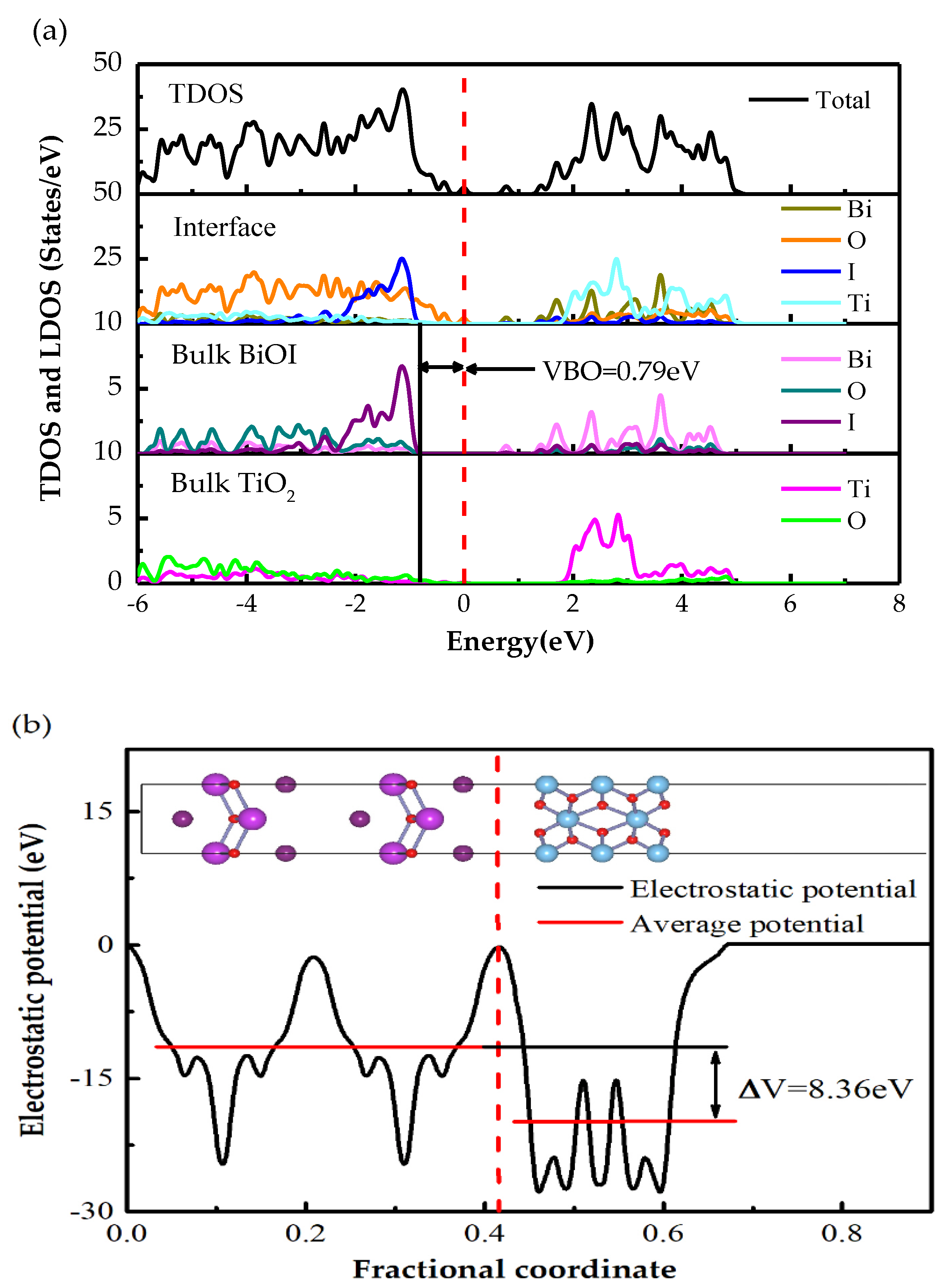
The DFT method calculated the density of states, including the TDOS and LDOS regarding bilateral layers far from the interface of the 1I-BiOI/TiO2 heterojunction that is plotted in Figure 5a. The bulk BiOI and bulk TiO2, shown in Figure 5a represents the layers far from the interface indicating that the electronic distribution is like that in independent materials. It can be seen from Figure 5a that the valence band and conduction band of bulk BiOI shows a larger shift to the lower energy. In addition, it can be perceived that the band-gap of bulk BiOI is about 1.39 eV, ranging from −0.79 to 0.60 eV, while bulk TiO2 has a band-gap of 1.91 eV, ranging from 0 to 1.91 eV. The band gap of bulk BiOI and TiO2 are reduced compared with pure BiOI (1.85 eV) and TiO2 (3.0 eV). A smaller band-gap of bulk BiOI and TiO2 will increase the excitation probability of photogenerated electrons, which can stimulate stronger visible light response and enhance the catalytic activity.
As shown in Figure 5b, the valence band maximum (VBM) of the interface is primarily contributed by TiO2. The difference VBM between BiOI and TiO2 is 0.79 eV. Therefore, the VBO between BiOI and TiO2 is 0.79 eV. Here, the CBO is deduced by utilizing the band gaps of BiOI and TiO2 from the experiment (3.0 eV for TiO2 and 1.85 eV for BiOI). The VBO is calculated by the following formula [37,38,39]:
represents the difference between the experimental optical bands gap of BiOI and TiO2. The CBO calculated by this formula is 1.94 eV.
is the difference of the VBM got from the pour structures of BiOI and TiO2 under the same pressure. is obtained through the calculation of the difference of the average of the electrostatic potential through the 1i-BiOI/TiO2 heterojunction.
The calculated electrostatic potentials of 1I-BiOI and TiO2 are plotted in Figure 5b. The solid red lines represent the average potential of BiOI and TiO2 parts. The average electrostatic potentials of BiOI and TiO2 are −11.60 eV and −19.96 eV respectively, indicating that is −8.36 eV. While the VBM of BiOI and TiO2 are −3.72 eV and 5.67 eV respectively indicating the calculated is 9.39 eV, so the deduced value of VBO is 1.03 eV. The deduced VBO calculated by the potential-line-up method is about 1.03 eV matching well with the value of the LDOS analysis. As shown in Figure 5b, a built-in potential about 28.3 eV is created around the interface of 1I-BiOI/TiO2 junction. Generally, the calculated VBO and CBO of 1I-BiOI/TiO2 heterojunction are 0.79 eV and 1.94 eV respectively, which indicates that the BOs between BiOI and TiO2 will enhance the separation of photogenerated electron-hole pairs and effectively avoid electron-hole recombination. Therefore, electrons could be transferred from the TiO2 to BiOI section and the holes will be transferred in the opposite direction. In addition, the huge difference of potential through the interface capacity to stimulate separation of electron-hole pairs to the farther ends and finally photocatalytic efficiency can be improved.
A substantial charge transfers through the interfaces of 1I-BiOI/TiO2 heterojunction. For making a thorough investigation into the electronic distribution and transfer of the 1I-BiOI/TiO2 heterojunction, the three-dimensional charge density difference (CDD) is used to analyze the properties of 1I-BiOI/TiO2 heterojunction. CDD can describe the “electronic map” vividly and intuitively. This practical method can be deduced by the following formula:
, and represent the electronic density of the 1I-BiOI/TiO2 heterojunction, the free-standing isolated TiO2 and the 1I-BiOI surface in the same configuration, respectively.
From Figure 6a, we found that there is a dramatic change of the electronic density around the interface owing to the combination of TiO2 and BiOI. Significant electronic accumulation is observed in the space above I (L-3) atoms in 1I-BiOI part, whereas a little charge depletion is found both on the bottom of Ti (L-2) atoms in the lowest side of the TiO2 part and the middle of the interface region of the 1I-BiOI/TiO2 heterojunction. The above analysis indicates that the electron transport violently occurs around the interface owing to the combination of BiOI and TiO2.
The Mulliken population can present the quantitative calculation of the electronic distribution for the 1I-BiOI/TiO2 heterojunction. Here, the Mulliken charge of two representative atoms (I and Ti atoms) is demonstrated in Figure 6b. As shown in Figure 6, the I (L-3) atom obtains a Mulliken charge of −0.30, which is greater than I atoms in other layers of 1I-BiOI part, clearly demonstrating that the electron of I atoms (L-3) increases by a very small amount in the 1I-BiOI/TiO2 heterojunction. The charge variation demonstrates that the I (L-3) atom in the top layer of the BiOI part would lose less electrons than I atoms inside the 1I-BiOI part. While the Mulliken charge of Ti (L-2) is 1.23, which is smaller than Ti atoms in other layers, indicating that the electron redistribution appears around the interface. I (L-3) atoms lose some electrons to Ti (L-4) atoms, indicating that the Mulliken charge analysis is consistent with the CDD analysis. Meanwhile, the built-in potential is created around the interface, and the built-in potential drive electronic transfer from the TiO2 part to 1I-BiOI part, which is consistent with the band offset analysis in Figure 5a.
3.2.3. Optical Properties and Photocatalytic Mechanism
The dielectric function provides a close connection between photons and electrons, and it reflects the linear response of materials to electromagnetic radiation [40]. Absorption spectra can be calculated according to the following formula [41]:
The calculated optical absorption spectra of pure BiOI, TiO2 and BiOI/TiO2 heterojunctions systems as the function of energy and wavelength are displayed in Figure 7. It can obtain that at the low-energy region from 0 to 1 eV, as shown in in Figure 7a, the optical absorption spectra of BiO–BiOI/TiO2 heterojunction has a small characteristic peak at 0.69 eV. The optical absorption amount of BiOI/TiO2 heterojunction is much higher than that of pure BiOI and TiO2 in the low-energy region. In addition, composing BiOI and TiO2 into a heterojunction makes the absorption edges redshift, and the BiO–BiOI/TiO2 heterojunction has a larger amount of redshift than 1I–BiOI/TiO2 heterojunction. The above analysis makes it clear that the BiOI/TiO2 heterojunction can dramatically enhance the performance of absorbing visible light, and finally improve the photocatalytic performance.
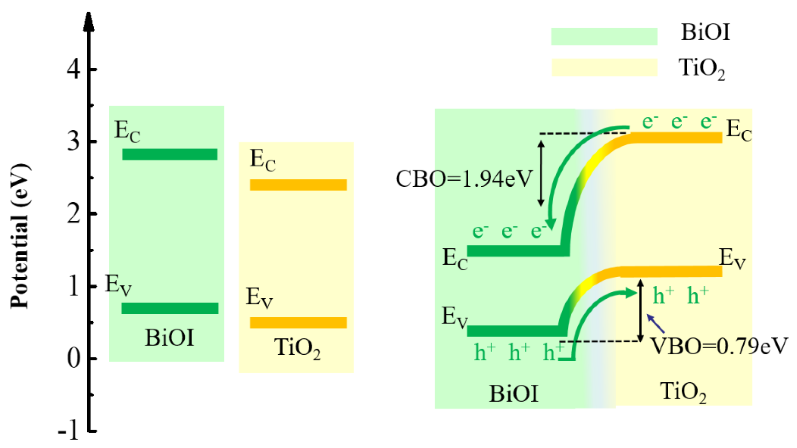
From the above analysis of the electronic structures and optical properties of the 1I–BiOI/TiO2 heterojunction, a schematic diagram of band structure for pre and post binding 1I–BiOI/TiO2 heterojunction is shown in Figure 8. We can obtain the conclusions as follows: BiOI with narrow band-gap (1.85 eV) can be tendentiously excited by most of visible light and promote the generation of photoelectrons and holes. However, the generated photo-induced electron-hole pairs of BiOI may recombine immediately due to the narrow band-gap and small sizes, which weakening its photocatalytic properties to a great extent. Because of the large band-gap of TiO2 (3.0 eV), TiO2 can only use a few parts of visible-light (energy >2.95 eV, wavelength <420 nm). As shown in the schematic diagram of Figure 8, when BiOI and TiO2 are contacted with each other constituting a heterojunction, BiOI will play a “photoelectric conversion driver” to absorb visible light. A large built-in potential about 28.3 eV, shown in Figure 5b, and it is created around the interface of the 1I-BiOI/TiO2 heterojunction. Therefore, electrons could be pumped from the TiO2 to the BiOI section and the holes will transfer in the opposite direction. Meanwhile, the built-in potential capacity will promote photogenerated electron-hole pairs separation on the contrary direction.
As a result, under the light condition (energy >1.85 eV), photogenic positive holes are stimulated in the VB of p-BiOI part priority. The reformed VB edge of BiOI is more inactive than that of TiO2 about 0.79 eV. Hence photo-induced holes on the VB of BiOI part would easily transfer to the VB of TiO2 part while leaving the photo-induced electrons on the CB of BiOI as shown in Figure 8. Electrons will be driven by transferring from CB of TiO2 to BiOI part driven by built-in potential through the surface at the same time. The formed built-in potential at the interface of 1I-BiOI/TiO2 heterojunction can significantly accelerate the transfer of photogenerated carriers and prevent its recombination dramatically. The existence of those well-separated photo-electrons and holes would better degrade molecules of organic pollutants. On the whole, the BiOI/TiO2 heterojunction possesses excellent photocatalytic properties under the degradation of organic pollutants condition under illumination.
4. Conclusions
The characteristics and properties of the 1I–BiOI/TiO2 heterojunction and the BiO–BiOI/TiO2 heterojunction are studied via the first-principles calculation based on the DFT theory. The structure of the BiOI/TiO2 changes slightly, and the interaction on the interface is van der Waals rather than covalent. The band structure of the BiOI/TiO2 heterojunction is modified a lot. The band-gap of the 1I–BiOI/TiO2 heterojunction reduces to 0.28 eV and the BiO–BiOI/TiO2 heterojunction changes into an n-type semiconductor. The calculated VBO of the 1I–BiOI/TiO2 heterojunction is 0.79 eV, and the CBO of the 1I–BiOI/TiO2 heterojunction is 1.94 eV respectively. The generated electron-hole pairs will be preferentially produced in the BiOI side under light, and then the holes are easily transferred through the interface from the VBM of the BiOI part to the VBM of the TiO2 part while leaving the electrons in the CBM of BiOI part. Meanwhile, the built-in potential can effectively speed up the separation of photo-generated electron-hole pairs and effectively avoid electron-hole recombination. Perfectly separated electron-hole pairs across the interface of the BiOI/TiO2 heterojunction will greatly improve its photocatalytic performance. The conclusions in this paper can provide a theoretical understanding of the BiOI/TiO2 heterojunction and the further utilization of visible-light response materials, such as BiOI-based semiconductor photocatalysts.
Author Contributions
Conceptualization, Z.Q., Y.S., L.S., F.L. and G.Z.; methodology, Z.Q., Y.S., L.S., F.L. and G.Z.; validation, Z.Q. and G.Z.; formal analysis, Y.S., L.S., F.L. and G.Z.; investigation, Z.Q. and Y.S.; resources, L.S., F.L. and G.Z.; data curation, Y.S. and G.Z.; writing—original draft preparation, Z.Q. and G.Z.; writing—review and editing, Y.S., L.S., F.L. and G.Z.; visualization, Z.Q., Y.S., L.S., F.L. and G.Z.; supervision, Y.S., L.S., F.L. and G.Z. All authors have read and agreed to the published version of the manuscript.
Funding
This research was funded by the National Science Foundation for the Young Scholars of China (Grant No. 61701531).
Conflicts of Interest
The authors declare no conflicts of interest.
References
- Yu, J.; Fan, J.; Zhao, L. Dye-sensitized solar cells based on hollow anatase TiO2 spheres prepared by self-transformation method. Electrochim. Acta 2010, 55, 597–602. [Google Scholar] [CrossRef]
- Jamal, R.; Osman, Y.; Rahman, A.; Ali, A.; Zhang, Y.; Abdiryim, T. Solid-State Synthesis and Photocatalytic Activity of Polyterthiophene Derivatives/TiO2 Nanocomposites. Materials 2014, 7, 3786–3801. [Google Scholar] [CrossRef] [PubMed] [Green Version]
- Hassan, M.E.; Chen, J.; Liu, G.; Zhu, D.; Cai, J. Enhanced Photocatalytic Degradation of Methyl Orange Dye under the Daylight Irradiation over CN-TiOâ Modified with OMS-2. Materials 2014, 7, 8024–8036. [Google Scholar] [CrossRef] [PubMed]
- Dai, G.; Yu, J.; Liu, G. Synthesis and enhanced visible-light photoelectrocatalytic activity of p-n junction BiOI/TiO2 nanotube arrays. J. Phys. Chem. C 2011, 115, 7339–7346. [Google Scholar] [CrossRef]
- Hoffmann, M.R.; Martin, S.T.; Choi, W.; Bahnemann, D.W. Environmental applications of semiconductor photocatalysis. Chem. Rev. 1995, 95, 69–96. [Google Scholar] [CrossRef]
- Yu, J.; Dai, G.; Xiang, Q.; Jaroniec, M. Fabrication and enhanced visible-light photocatalytic activity of carbon self-doped TiO2 sheets with exposed {001} facets. J. Mater. Chem. 2011, 21, 1049–1057. [Google Scholar] [CrossRef]
- Xiang, Q.; Yu, J.; Cheng, B.; Ong, H. Microwave-hydrothermal preparation and visible-light photoactivity of plasmonic photocatalyst Ag-TiO2 nanocomposite hollow spheres. Chem. Asian J. 2010, 5, 1466–1474. [Google Scholar] [CrossRef]
- Berger, T.; Sterrer, M.; Diwald, O.; Knözinger, E.; Panayotov, D.; Thompson, T.L.; Yates, J.T. Light-induced charge separation in anatase TiO2 particles. J. Phys. Chem. B 2005, 109, 6061–6068. [Google Scholar] [CrossRef]
- Kumar, S.; Fedorov, A.G.; Gole, J.L. Photodegradation of ethylene using visible light responsive surfaces prepared from titania nanoparticle slurries. Appl. Catal. B Environ. 2005, 57, 93–107. [Google Scholar] [CrossRef]
- Sun, W.-T.; Yu, Y.; Pan, H.-Y.; Gao, X.-F.; Chen, Q.; Peng, L.-M. CdS quantum dots sensitized TiO2 nanotube-array photoelectrodes. J. Am. Chem. Soc. 2008, 130, 1124–1125. [Google Scholar] [CrossRef]
- Baker, D.R.; Kamat, P.V. Photosensitization of TiO2 nanostructures with CdS quantum dots: Particulate versus tubular support architectures. Adv. Funct. Mater. 2009, 19, 805–811. [Google Scholar] [CrossRef]
- Zhang, H.; Quan, X.; Chen, S.; Yu, H.; Ma, N. “Mulberry-like” CdSe nanoclusters anchored on TiO2 nanotube arrays: A novel architecture with remarkable photoelectrochemical performance. Chem. Mater. 2009, 21, 3090–3095. [Google Scholar] [CrossRef]
- Kongkanand, A.; Tvrdy, K.; Takechi, K.; Kuno, M.; Kamat, P.V. Quantum dot solar cells. Tuning photoresponse through size and shape control of CdSe-TiO2 architecture. J. Am. Chem. Soc. 2008, 130, 4007–4015. [Google Scholar] [CrossRef] [PubMed]
- Janczarek, M.; Endo, M.; Zhang, D.; Wang, K.; Kowalska, E. Enhanced Photocatalytic and Antimicrobial Performance of Cuprous Oxide/Titania: The Effect of Titania Matrix. Materials 2018, 11, 2069. [Google Scholar] [CrossRef] [PubMed] [Green Version]
- Hou, Y.; Li, X.; Zou, X.; Quan, X.; Chen, G. Photoeletrocatalytic activity of a Cu2O-loaded self-organized highly oriented TiO2 nanotube array electrode for 4-chlorophenol degradation. Environ. Sci. Techonl. 2008, 43, 858–863. [Google Scholar] [CrossRef]
- Chiou, Y.-K.; Chang, C.-H.; Wang, C.-C.; Lee, K.-Y.; Wu, T.-B.; Kwo, R.; Hong, M. Effect of Al incorporation in the thermal stability of atomic-layer-deposited HfO2 for gate dielectric applications. J. Electrochem. Soc. 2007, 154, G99–G102. [Google Scholar] [CrossRef]
- Xu, H.; Ouyang, S.; Liu, L.; Reunchan, P.; Umezawa, N.; Ye, J. Recent advances in TiO2-based photocatalysis. J. Mater. Chem. A 2014, 2, 12642–12661. [Google Scholar] [CrossRef]
- Zhang, X.; Ai, Z.; Jia, F.; Zhang, L. Generalized one-pot synthesis, characterization, and photocatalytic activity of hierarchical BiOX (X = Cl, Br, I) nanoplate microspheres. J. Phys. Chem. C 2008, 112, 747–753. [Google Scholar] [CrossRef]
- Cheng, H.; Huang, B.; Dai, Y. Engineering BiOX (X = Cl, Br, I) nanostructures for highly efficient photocatalytic applications. Nanoscale 2014, 6, 2009–2026. [Google Scholar] [CrossRef]
- Cao, J.; Xu, B.; Luo, B.; Lin, H.; Chen, S. Novel BiOI/BiOBr heterojunction photocatalysts with enhanced visible light photocatalytic properties. Catal. Commun. 2011, 13, 63–68. [Google Scholar] [CrossRef]
- Xiao, X.; Zhang, W.-D. Facile synthesis of nanostructured BiOI microspheres with high visible light-induced photocatalytic activity. J. Mater. Chem. 2010, 20, 5866–5870. [Google Scholar] [CrossRef]
- Cao, J.; Xu, B.; Lin, H.; Luo, B.; Chen, S. Novel heterostructured Bi2S3/BiOI photocatalyst: Facile preparation, characterization and visible light photocatalytic performance. Dalton Trans. 2012, 41, 11482–11490. [Google Scholar] [CrossRef] [PubMed]
- Zhang, X.; Zhang, L.; Xie, T.; Wang, D. Low-temperature synthesis and high visible-light-induced photocatalytic activity of BiOI/TiO2 heterostructures. J. Phys. Chem. C 2009, 113, 7371–7378. [Google Scholar] [CrossRef]
- Segall, M.; Lindan, P.J.; Probert, M.A.; Pickard, C.J.; Hasnip, P.J.; Clark, S.; Payne, M. First-principles simulation: Ideas, illustrations and the CASTEP code. J. Phys. Condens. Matter 2002, 14, 2717. [Google Scholar] [CrossRef]
- Perdew, J.P.; Burke, K.; Ernzerhof, M. Generalized gradient approximation made simple. Phys. Rev. Lett. 1996, 77, 3865. [Google Scholar] [CrossRef] [Green Version]
- Monkhorst, H.J.; Pack, J.D. Special points for Brillouin-zone integrations. Phys. Rev. B 1976, 13, 5188. [Google Scholar] [CrossRef]
- Shanno, D.F.; Phua, K.-H. Matrix conditioning and nonlinear optimization. Math. Program. 1978, 14, 149–160. [Google Scholar] [CrossRef]
- Colombo, L.; Resta, R.; Baroni, S. Valence-band offsets at strained Si/Ge interfaces. Phys. Rev. B 1991, 44, 5572. [Google Scholar] [CrossRef]
- Yu, C.; Fan, C.; Jimmy, C.Y.; Zhou, W.; Yang, K. Preparation of bismuth oxyiodides and oxides and their photooxidation characteristic under visible/UV light irradiation. Mater. Res. Bull. 2011, 46, 140–146. [Google Scholar] [CrossRef]
- Zhao, L.; Zhang, X.; Fan, C.; Liang, Z.; Han, P. First-principles study on the structural, electronic and optical properties of BiOX (X = Cl, Br, I) crystals. Physica B 2012, 407, 3364–3370. [Google Scholar] [CrossRef]
- Kong, T.; Wei, X.; Zhu, G.; Huang, Y. First-principles studies on facet-dependent photocatalytic properties of BiOI {001} surface. J. Mater. Sci. 2017, 52, 5686–5695. [Google Scholar] [CrossRef]
- Finnis, M.; Lozovoi, A.; Alavi, A. The oxidation of NiAl: What can we learn from ab initio calculations? Rev. Mater. Res. 2005, 35, 167–207. [Google Scholar] [CrossRef] [Green Version]
- Bass, J.; Oloumi, M.; Matthai, C.C. A method for determining band offsets in semiconductor superlattices and interfaces. J. Phys. Condens. Matter 1989, 1, 10625. [Google Scholar] [CrossRef]
- Robertson, J.; Peacock, P. Bonding and structure of some high-k oxide: Si interfaces. Phys. Status Solidi B 2004, 241, 2236–2245. [Google Scholar] [CrossRef]
- Baldereschi, A.; Baroni, S.; Resta, R. Band offsets in lattice-matched heterojunctions: A model and first-principles calculations for GaAs/AlAs. Phys. Rev. Lett. 1988, 61, 734. [Google Scholar] [CrossRef]
- Junquera, J.; Cohen, M.H.; Rabe, K.M. Nanoscale smoothing and the analysis of interfacial charge and dipolar densities. J. Phys Condens. Matter 2007, 19, 213203. [Google Scholar] [CrossRef]
- Cao, R.; Zhang, Z.; Wang, C.; Li, H.; Xie, X.; Dong, H.; Liu, H.; Wang, W. Interfacial bonding and electronic structure of GaN/GaAs interface: A first-principles study. J. Phys. D Appl. Phys. 2015, 117, 135302. [Google Scholar] [CrossRef]
- Yang, W.; Wen, Y.; Zeng, D.; Wang, Q.; Chen, R.; Wang, W.; Shan, B. Interfacial charge transfer and enhanced photocatalytic performance for the heterojunction WO3/BiOCl: First-principles study. J. Mater. Chem. A 2014, 2, 20770–20775. [Google Scholar] [CrossRef]
- Peressi, M.; Binggeli, N.; Baldereschi, A. Band engineering at interfaces: Theory and numerical experiments. J. Phys. D Appl. Phys. 1998, 31, 1273. [Google Scholar] [CrossRef]
- Lovell, R. Application of Kramers-Kronig relations to the interpretation of dielectric data. J. Phys. C. Solid State Phys. 1974, 7, 4378–4384. [Google Scholar] [CrossRef]
- Saha, S.; Sinha, T.P.; Mookerjee, A. Electric Structure, Chemical Bonding, and Optical Properties of Paraelectric BaTiO3. Phys. Rev. B 2000, 62, 699–702. [Google Scholar] [CrossRef]
Figure 1.
Crystal models: (a) BiOI, (b) rutile-TiO2, finally relaxed configuration of (c) 1I-BiOI/TiO2 and (d) BiO-BiOI/TiO2 heterojunction. Purple, red, brown and blue spheres represent Bi, O, I and Ti atoms respectively. L-1 to L-4 represent atomic layer from layer-1 to layer-4.
Figure 1.
Crystal models: (a) BiOI, (b) rutile-TiO2, finally relaxed configuration of (c) 1I-BiOI/TiO2 and (d) BiO-BiOI/TiO2 heterojunction. Purple, red, brown and blue spheres represent Bi, O, I and Ti atoms respectively. L-1 to L-4 represent atomic layer from layer-1 to layer-4.

Figure 2.
The band structures of relaxed (a) 1I-BiOI/TiO2, (b) BiO-BiOI/TiO2 heterojunction. Red dashed line represents the Fermi level.
Figure 2.
The band structures of relaxed (a) 1I-BiOI/TiO2, (b) BiO-BiOI/TiO2 heterojunction. Red dashed line represents the Fermi level.

Figure 3.
The band structures of 1I-BiOI/TiO2 heterojunction under (a) −2%, (b) −1%, (c) 1% and (d) 2% {001} IPBTSs. Red dashed line represents the Fermi level.
Figure 3.
The band structures of 1I-BiOI/TiO2 heterojunction under (a) −2%, (b) −1%, (c) 1% and (d) 2% {001} IPBTSs. Red dashed line represents the Fermi level.

Figure 4.
The total and partial density of states of (a) 1I-BiOI/TiO2, (b) BiO-BiOI/TiO2 heterojunctions. Red dashed line represents the Fermi level.
Figure 4.
The total and partial density of states of (a) 1I-BiOI/TiO2, (b) BiO-BiOI/TiO2 heterojunctions. Red dashed line represents the Fermi level.

Figure 5.
(a) The total and local density of states, (b) electrostatic potential of the 1I-BiOI/TiO2 heterojunction.
Figure 5.
(a) The total and local density of states, (b) electrostatic potential of the 1I-BiOI/TiO2 heterojunction.

Figure 6.
(a) 3D charge density difference for the 1I-BiOI/TiO2 heterojunction with an isovalue of 0.01 e/Å3. Yellow and cyan isosurfaces represent charge accumulation and depletion in the space respectively. (b) Mulliken population charge distribution maps of 1I-BiOI/TiO2 heterojunction.
Figure 6.
(a) 3D charge density difference for the 1I-BiOI/TiO2 heterojunction with an isovalue of 0.01 e/Å3. Yellow and cyan isosurfaces represent charge accumulation and depletion in the space respectively. (b) Mulliken population charge distribution maps of 1I-BiOI/TiO2 heterojunction.

Figure 7.
The absorption spectra of pure BiOI, TiO2, and BiOI/TiO2 heterojunction as the function of (a) energy and (b) wavelength using the DFT method.
Figure 7.
The absorption spectra of pure BiOI, TiO2, and BiOI/TiO2 heterojunction as the function of (a) energy and (b) wavelength using the DFT method.


Figure 8.
Schematic diagram of the 1I–BiOI/TiO2 heterojunction and its energy band distribution.


Table 1.
The calculated bond distance (Å) and bond population (e) for the atoms at the interface of the BiOI/TiO2 heterojunction.
Table 1.
The calculated bond distance (Å) and bond population (e) for the atoms at the interface of the BiOI/TiO2 heterojunction.
| System | Bond | Bond Distance (Å) | Bond Population (e) | |
|---|---|---|---|---|
| Before Relaxation | After Relaxation | |||
| 1I-BiOI/TiO2 | Ti (L-2)-I (L-3) | 4.06 | 4.80 | 0 |
| O (L-2)-I (L-3) | 3.48 | 4.23 | 0 | |
| BiO-BiOI/TiO2 | Ti (L-2)-O (L-4) | 3.57 | 3.34 | 0 |
| O (L-2)-Bi (L-4) | 2.82 | 2.69 | 0.08 | |
© 2020 by the authors. Licensee MDPI, Basel, Switzerland. This article is an open access article distributed under the terms and conditions of the Creative Commons Attribution (CC BY) license (http://creativecommons.org/licenses/by/4.0/).
Share and Cite
MDPI and ACS Style
Qu, Z.; Su, Y.; Sun, L.; Liang, F.; Zhang, G. Study of the Structure, Electronic and Optical Properties of BiOI/Rutile-TiO2 Heterojunction by the First-Principle Calculation. Materials 2020, 13, 323. https://doi.org/10.3390/ma13020323
AMA Style
Qu Z, Su Y, Sun L, Liang F, Zhang G. Study of the Structure, Electronic and Optical Properties of BiOI/Rutile-TiO2 Heterojunction by the First-Principle Calculation. Materials. 2020; 13(2):323. https://doi.org/10.3390/ma13020323
Chicago/Turabian StyleQu, Zhan, Yali Su, Li Sun, Feng Liang, and Guohe Zhang. 2020. "Study of the Structure, Electronic and Optical Properties of BiOI/Rutile-TiO2 Heterojunction by the First-Principle Calculation" Materials 13, no. 2: 323. https://doi.org/10.3390/ma13020323
Note that from the first issue of 2016, this journal uses article numbers instead of page numbers. See further details here.