
A Review of Diagnostics Methodologies for Metal Additive Manufacturing Processes and Products

 , ,
, ,
Abstract
:| Table of Contents | |
| 1. Introduction: Metal Additive Manufacturing (AM) Technologies | 2 |
| 1.1 Fusion-Based AM Techniques | 2 |
| 1.2. Solid-State AM Techniques | 4 |
| 1.3. Mixed-Phase (Solid–Liquid) AM Techniques | 5 |
| 1.4. Surface Engineering via AM Techniques | 6 |
| 1.5. Comparison and Significance of AM versus Conventional Manufacturing | 7 |
| 2. Electron-Based Characterization and Diagnostics | 8 |
| 2.1 Electron Beam-Based Diagnosis/Characterization | 8 |
| 2.2. X-ray-Based Diagnosis/Characterization | 10 |
| 2.3. Electron–X-ray Combined Characterization Techniques | 10 |
| 3. Thermal Imaging | 13 |
| 3.1. Two-Wavelength Thermal Imaging under the Grey Body Approximation | 13 |
| 3.2. When the Grey Body Approximation Fails | 15 |
| 3.3. Discussion on Thermal Imaging | 16 |
| 4. Ultrasonic Inspection and Evaluation | 17 |
| 4.1. Ultrasonic Diagnostics | 17 |
| 4.2. Non-Destructive Ultrasonic Elasticity Measurement and Elastography | 24 |
| 4.3. Longitudinal and Transversal Sound Velocity Elasticity Measurement | 25 |
| 4.4. Comparison of Various Ultrasonic Techniques | 29 |
| 5. Mechanical Test | 30 |
| 5.1. Elasticity Test with Information on Plasticity | 30 |
| 5.2. Mechanical Test Provides Only Plasticity | 35 |
| 5.3. Impact Test | 37 |
| 5.4. Fatigue Test | 38 |
| 5.5. Advantages and Disadvantages, Comparison and Discussion of Mechanical Testing | 39 |
| 6. Laser-Induced Breakdown Spectroscopy | 39 |
| 7. Other Diagnostic Methods | 41 |
| 8. Conclusions and Discussion | 42 |
| Reference | 43 |
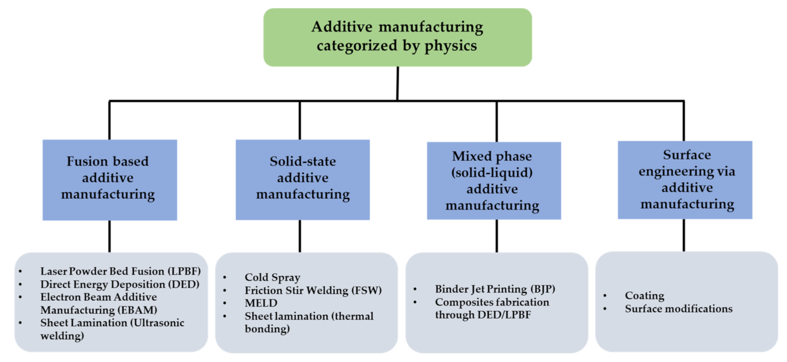
1. Introduction: Metal Additive Manufacturing (AM) Technologies
1.1. Fusion-Based AM Techniques
1.2. Solid-State AM Techniques
1.3. Mixed-Phase (Solid–Liquid) AM Techniques
1.4. Surface Engineering via AM Techniques
1.5. Comparison and Significance of AM versus Conventional Manufacturing
2. Electron-Based Characterization and Diagnostics
2.1. Electron Beam-Based Diagnosis/Characterization

| Electron-Based Analysis Method | Working Principle | Measuring Process | Measuring Characteristics |
|---|---|---|---|
| Scanning Electron Microscopy (TEM) | Detecting secondary and backscattered electrons resulting from sample and electron beam interactions | Electrons in range of 1–30 kV are applied to the sample, and secondary, backscattered electrons are detected | Measuring fine surface morphology and phase differentiation. Observing cross-section of samples. Resolving power can be ~1 nm |
| Transmission Electron Microscopy (TEM) | Primary electron traverse through sample, producing both transmitted and diffracted electron beam | Transmission of electrons in range of 100–1000 kV through a sample and detection of absorption and diffracted electrons by the interactions between atoms | Fine crystal defects, grain size, lattice structure. Resolving power can be around 2 nm |
| Electron Energy Loss Spectroscopy (EELS) | Electron beam–sample interactions result in inelastic scattering of electrons | A coherent electron beam incident on a sample produces inelastically scattered electrons having lesser energy. These inelastically scattered electrons are measured. | Atomic compositions, surface properties, chemical bonding in sample |
| Auger Electron Spectroscopy (AES) | Primary electrons incident on the sample surface and resulting in Auger electrons | Auger electrons, unique to each atom and resulting from electron beam and sample interaction, are measured | Composition analysis and impurities detection |
2.2. X-ray-Based Diagnosis/Characterization
2.3. Electron–X-ray Combined Characterization Techniques
3. Thermal Imaging
3.1. Two-Wavelength Thermal Imaging under the Grey Body Approximation
3.2. When the Grey Body Approximation Fails
3.3. Discussion on Thermal Imaging
4. Ultrasonic Inspection and Evaluation
4.1. Ultrasonic Diagnostics
- –
- requiring a minimal part preparation procedure;
- –
- not applying plastic deformation on the test material;
- –
- good penetration depth;
- –
- instant results.
- –
- The disadvantages of the ultrasonic technique include:
- –
- the surface must be accessible for ultrasound transmission;
- –
- specific knowledge and training for operation;
- –
- due to low sound transmission and weak signal–noise ratio, inspection at high frequencies is challenging due to the large grain size in cast raw material;
- –
- standards of reference are needed for both calibration of equipment and defect characterization.
4.2. Non-Destructive Ultrasonic Elasticity Measurement and Elastography
4.3. Longitudinal and Transversal Sound Velocity Elasticity Measurement
4.4. Comparison of Various Ultrasonic Techniques
5. Mechanical Test
5.1. Elasticity Test with Information on Plasticity
5.2. Mechanical Test Provides Only Plasticity
5.3. Impact Test
5.4. Fatigue Test
5.5. Advantages and Disadvantages, Comparison and Discussion of Mechanical Testing
6. Laser-Induced Breakdown Spectroscopy
7. Other Diagnostic Methods
8. Conclusions and Discussion
Author Contributions
Funding
Institutional Review Board Statement
Informed Consent Statement
Data Availability Statement
Conflicts of Interest
References
- Berman, B. 3D printing: The new industrial revolution. IEEE Eng. Manag. Rev. 2013, 41, 72–80. [Google Scholar] [CrossRef]
- Carroll, B.E.; Palmer, T.A.; Beese, A.M. Anisotropic tensile behavior of Ti–6Al–4V components fabricated with directed energy deposition additive manufacturing. Acta Mater. 2015, 87, 309–320. [Google Scholar] [CrossRef]
- Brandl, E.; Palm, F.; Michailov, V.; Viehweger, B.; Leyens, C. Mechanical properties of additive manufactured titanium (Ti–6Al–4V) blocks deposited by a solid-state laser and wire. Mater. Des. 2011, 32, 4665–4675. [Google Scholar] [CrossRef]
- Bourell, D.L.; Rosen, D.W.; Leu, M.C. The roadmap for additive manufacturing and its impact. 3D Print. Addit. Manuf. 2014, 1, 6–9. [Google Scholar] [CrossRef]
- Kumar, L.J.; Pandey, P.M.; Wimpenny, D.I. (Eds.) 3D Printing and Addit. Manuf. Technologies; Springer: Singapore, 2019. [Google Scholar]
- Beaman, J.J.; Deckard, C.R. Selective Laser Sintering with Assisted Powder Handling. US Patent 5,053,090, 3 July 1991. [Google Scholar]
- Rännar, L.E.; Glad, A.; Gustafson, C.G. Efficient cooling with tool inserts manufactured by electron beam melting. Rapid Prototyp. J. 2007, 13, 128–135. [Google Scholar] [CrossRef]
- Kruth, J.-P.; Vandenbroucke, B.; Van Vaerenbergh, J.; Naert, I. Rapid manufacturing of dental prostheses by means of selective laser sintering/melting. Proc. AFPR S 2005, 4, 176–186. [Google Scholar]
- Murr, L.E.; Gaytan, S.M.; Ramirez, D.A.; Martinez, E.; Hernandez, J.; Amato, K.N.; Shindo, P.W.; Medina, F.R.; Wicker, R.B. Metal fabrication by Additive Manufacturing using laser and electron beam melting technologies. J. Mater. Sci. Technol. 2012, 28, 1–14. [Google Scholar] [CrossRef]
- Appleyard, D. Powering up on powder technology. Met. Powder Rep. 2015, 70, 285–289. [Google Scholar] [CrossRef]
- Basak, A.; Das, S. Epitaxy and microstructure evolution in metal additive manufacturing. Annu. Rev. Mater. Res. 2016, 46, 125–149. [Google Scholar] [CrossRef]
- Frazier, W.E. Metal additive manufacturing: A review. J. Mater. Eng. Perform. 2014, 23, 1917–1928. [Google Scholar] [CrossRef]
- Louvis, E.; Fox, P.; Sutcliffe, C.J. Selective laser melting of aluminium components. J. Mater. Process. Technol. 2011, 211, 275–284. [Google Scholar] [CrossRef]
- Bhardwaj, T.; Shukla, M.; Paul, C.P.; Bindra, K.S. Direct energy deposition-laser additive manufacturing of titanium-molybdenum alloy: Parametric studies, microstructure and mechanical properties. J. Alloy. Compd. 2019, 787, 1238–1248. [Google Scholar] [CrossRef]
- Yin, S.; Cavaliere, P.; Aldwell, B.; Jenkins, R.; Liao, H.; Li, W.; Lupoi, R. Cold spray additive manufacturing and repair: Fundamentals and applications. Addit. Manuf. 2018, 21, 628–650. [Google Scholar] [CrossRef]
- Mishra, R.S.; Ma, Z.Y. Friction stir welding and processing. Mater. Sci.Eng. R Rep. 2005, 50, 1–78. [Google Scholar] [CrossRef]
- Champagne, V.; Helfritch, D. The unique abilities of cold spray deposition. Int. Mater. Rev. 2016, 61, 437–455. [Google Scholar] [CrossRef]
- Mishra, R.S.; Ma, Z.Y.; Charit, I. Friction stir processing: A novel technique for fabrication of surface composite. Mater. Sci.Eng. A 2003, 341, 307–310. [Google Scholar] [CrossRef]
- Hardwick, N.; Cox, C.; Schultz, J.P.; Kandasamy, K. Meld Solid-State Joining of Different Features to Cast Parts. U.S. Patent 16/115,044, 20 December 2018. [Google Scholar]
- Griffiths, R.J.; Perry, M.E.; Sietins, J.M.; Zhu, Y.; Hardwick, N.; Cox, C.D.; Rauch, H.A.; Hang, Z.Y. A Perspective on Solid-State *additive manufacturing of Aluminum Matrix Composites Using MELD. J. Mater. Eng. Perform. 2019, 28, 648–656. [Google Scholar] [CrossRef]
- Gibson, I.; Rosen, D.W.; Stucker, B. Sheet lamination processes. Addit. Manuf. Technologies 2010, 223–252. [Google Scholar]
- Hu, Y.; Cong, W. A review on laser deposition-additive manufacturing of ceramics and ceramic reinforced metal matrix composites. Ceram. Int. 2018, 44, 20599–20612. [Google Scholar] [CrossRef]
- Kunze, J.M.; Gigerenzer, H.; Hu, C. Laser Fabrication of Discontinuously Reinforced Metal Matrix Composites. U.S. Patent 7,521,017, 21 April 2009. [Google Scholar]
- Ozden, S.; Ekici, R.; Nair, F. Investigation of impact behaviour of aluminium based SiC particle reinforced metal–matrix composites. Compos. Part A Appl. Sci. Manuf. 2007, 38, 484–494. [Google Scholar] [CrossRef]
- Sames, W.J.; List, F.A.; Pannala, S.; Dehoff, R.R.; Babu, S.S. The metallurgy and processing science of metal additive manufacturing. Int. Mater. Rev. 2016, 61, 315–360. [Google Scholar] [CrossRef]
- Matthews, M.J.; Guss, G.; Khairallah, S.A.; Rubenchik, A.M.; Depond, P.J.; King, W.E. Denudation of metal powder layers in laser powder bed fusion processes. Acta Mater. 2016, 114, 33–42. [Google Scholar] [CrossRef] [Green Version]
- Dobbelstein, H.; Thiele, M.; Gurevich, E.L.; George, E.P.; Ostendorf, A. Direct metal deposition of refractory high entropy alloy MoNbTaW. Phys. Procedia 2016, 83, 624–633. [Google Scholar] [CrossRef] [Green Version]
- Nandwana, P.; Elliott, A.M.; Siddel, D.; Merriman, A.; Peter, W.H.; Babu, S.S. Powder bed binder jet 3D printing of Inconel 718: Densification, microstructural evolution and challenges☆. Curr. Opin. Solid State Mater. Sci. 2017, 21, 207–218. [Google Scholar] [CrossRef]
- Paris, H.; Mokhtarian, H.; Coatanéa, E.; Museau, M.; Ituarte, I.F. Comparative environmental impacts of additive and subtractive manufacturing technologies. CIRP Ann. 2016, 65, 29–32. [Google Scholar] [CrossRef]
- Egerton, R.F. Electron Energy-Loss Spectroscopy in the Electron Microscope; Springer Science & Business Media: Berlin, Germany, 2011. [Google Scholar]
- Auger, P. The auger effect. Surf. Sci. 1975, 48, 1–8. [Google Scholar] [CrossRef]
- Oura, K.; Lifshits, V.G.; Saranin, A.A.; Zotov, A.V.; Katayama, M. Surface science: An introduction; Springer Science & Business Media: Berlin, Germany, 2013. [Google Scholar]
- Briggs, D. Practical Surface Analysis: Auger and X-ray Photoelectron Spectroscopy; John Wiley & Sons: Hoboken, NJ, USA, 1990; Volume 1, pp. 151–152. [Google Scholar]
- Epp, J. X-ray diffraction (XRD) techniques for materials characterization. In Materials Characterization using Nondestructive Evaluation (NDE) Methods; Woodhead Publishing: Sawston, UK, 2016; pp. 81–124. [Google Scholar]
- Boisse, P. (Ed.) Advances in Composites Manufacturing and Process Design; Woodhead Publishing: Sawston, UK, 2015. [Google Scholar]
- onda, R.W.; Lauridsen, E.M.; Ludwig, W.; Tafforeau, P.; Spanos, G. Two-dimensional and three-dimensional analyses of sigma precipitates and porosity in a superaustenitic stainless steel. Metall. Mater. Trans. A 2007, 38, 2721–2726. [Google Scholar]
- Humphreys, F.J. Characterisation of fine-scale microstructures by electron backscatter diffraction (EBSD). Scr. Mater. 2004, 51, 771–776. [Google Scholar] [CrossRef]
- Dahotre, N.B.; Vora, H.D.; Boesl, B. additive manufacturing via Surface Engineering. JOM 2016, 68, 1759–1761. [Google Scholar] [CrossRef]
- Book, T.A.; Sangid, M.D. Evaluation of select surface processing techniques for in situ application during the additive manufacturing build process. JOM 2016, 68, 1780–1792. [Google Scholar] [CrossRef]
- Ocelík, V.; Janssen, N.; Smith, S.N.; De Hosson, J.T.M. additive manufacturing of high-entropy alloys by laser processing. JOM 2016, 68, 1810–1818. [Google Scholar] [CrossRef] [Green Version]
- Attaran, M. The rise of 3-D printing: The advantages of additive manufacturing over traditional manufacturing. Bus. Horiz. 2017, 60, 677–688. [Google Scholar] [CrossRef]
- Pereira, T.; Kennedy, J.V.; Potgieter, J. A comparison of traditional manufacturing vs additive manufacturing, the best method for the job. Procedia Manuf. 2019, 30, 11–18. [Google Scholar] [CrossRef]
- Ahn, D.-G. Direct metal additive manufacturing processes and their sustainable applications for green technology: A review. Int. J. Precis. Eng. Manuf.-Green Technol. 2016, 3, 381–395. [Google Scholar] [CrossRef]
- Yamashita, T.; Hayes, P. Analysis of XPS spectra of Fe2+ and Fe3+ ions in oxide materials. Appl. Surf. Sci. 2008, 254, 2441–2449. [Google Scholar] [CrossRef]
- Bagus, P.S.; Ilton, E.S.; Nelin, C.J. The interpretation of XPS spectra: Insights into materials properties. Surf. Sci. Rep. 2013, 68, 273–304. [Google Scholar] [CrossRef]
- Thijs, L.; Verhaeghe, F.; Craeghs, T.; Humbeeck, J.V.; Kruth, J.-P. A study of the microstructural evolution during selective laser melting of Ti–6Al–4V. Acta Mater. 2010, 58, 3303–3312. [Google Scholar] [CrossRef]
- Tan, X.; Kok, Y.; Tan, Y.J.; Descoins, M.; Mangelinck, D.; Tor, S.B.; Leong, K.F.; Chua, C.K. Graded microstructure and mechanical properties of additive manufactured Ti–6Al–4V via electron beam melting. Acta Mater. 2015, 97, 1–16. [Google Scholar] [CrossRef]
- Gong, X.; Anderson, T.; Chou, K. Review on powder-based electron beam additive manufacturing technology. In ASME/ISCIE 2012 International Symposium on flexible Automation; American Society of Mechanical Engineers: Saint Louis, Mo, NY, USA, 2012; pp. 507–515. [Google Scholar]
- Goldstein, J.I.; Newbury, D.E.; Michael, J.R.; Ritchie, N.W.; Scott, J.H.J.; Joy, D.C. Scanning Electron Microscopy and X-ray Microanalysis; Springer: Berlin, Germany, 2017. [Google Scholar]
- Kanaya, K.; Kawakatsu, H. Secondary electron emission due to primary and backscattered electrons. J. Phys. D Appl. Phys. 1972, 5, 1727. [Google Scholar] [CrossRef]
- Inkson, B.J. Scanning electron microscopy (SEM) and transmission electron microscopy (TEM) for materials characterization. In Materials Characterization using Nondestructive Evaluation (NDE) Methods; Woodhead Publishing: Sawston, UK, 2016; pp. 17–43. [Google Scholar]
- Hofer, F.; Schmidt, F.-P.; Grogger, W.; Kothleitner, G. Fundamentals of electron energy-loss spectroscopy. IOP Conf. Ser. Mater. Sci. Eng. 2016, 109, 012007. [Google Scholar] [CrossRef]
- Kempen, K.; Yasa, E.; Thijs, L.; Kruth, J.-P.; Humbeeck, J.V. Microstructure and mechanical properties of Selective Laser Melted 18Ni-300 steel. Phys. Procedia 2011, 12, 255–263. [Google Scholar] [CrossRef] [Green Version]
- Palm, F.; Schmidtke, K. Exceptional grain refinement in directly built up Sc-modified AlMg-alloys is promising a quantum leap in ultimate light weight design. In Proceedings of the Trends in Welding Research 2012: Proceedings of the 9th International Conference, Chicago, IL, USA, 4–8 June 2013; p. 108. [Google Scholar]
- Liu, F.; Lin, X.; Yang, G.; Song, M.; Chen, J.; Huang, W. Microstructure and residual stress of laser rapid formed Inconel 718 nickel-base superalloy. Opt. Laser Technol. 2011, 43, 208–213. [Google Scholar] [CrossRef]
- Wu, B.; Pan, Z.; Li, S.; Cuiuri, D.; Ding, D.; Li, H. The anisotropic corrosion behaviour of wire arc additive manufactured Ti-6Al-4V alloy in 3.5% NaCl solution. Corros. Sci. 2018, 137, 176–183. [Google Scholar] [CrossRef]
- Yang, J.; Yang, H.; Yu, H.; Wang, Z.; Zeng, X. Corrosion behavior of additive manufactured Ti-6Al-4V alloy in NaCl solution. Metall. Mater. Trans. A 2017, 48, 3583–3593. [Google Scholar] [CrossRef]
- Alhuzaim, A.; Imbrogno, S.; Attallah, M.M. Controlling microstructural and mechanical properties of direct laser deposited Inconel 718 via laser power. J. Alloy. Compd. 2021, 872, 159588. [Google Scholar] [CrossRef]
- Ettefagh, A.H.; Zeng, C.; Guo, S.; Raush, J. Corrosion behavior of additively manufactured Ti-6Al-4V parts and the effect of post annealing. Addit. Manuf. 2019, 28, 252–258. [Google Scholar]
- Adelantado, J.G.; Eres, M.F.; Algarra, F.V.; Vicente, J.P.; Reig, F.B. Analytical study by SEM/EDX and metallographic techniques of materials used in the iron production process during the Iberian period. Talanta 2003, 60, 895–910. [Google Scholar] [CrossRef]
- Laigo, J.; Christien, F.; Le Gall, R.; Tancret, F.; Furtado, J. SEM, EDS, EPMA-WDS and EBSD characterization of carbides in HP type heat resistant alloys. Mater. Charact. 2008, 59, 1580–1586. [Google Scholar] [CrossRef]
- Diawara, Y.; Durst, R.D.; Medved, S.A.; Sedov, V.N.; Lesher, D.P. X-ray Detection System for Wavelength Dispersive and Energy Dispersive Spectroscopy and Electron Beam Applications. U.S. Patent 7,928,400, 19 April 2011. [Google Scholar]
- Lütjering, G.; Williams, J.C. Titanium; Springer: Berlin, Germany, 2003; p. 17. [Google Scholar]
- Yang, Q.; Xia, C.; Deng, Y.; Li, X.; Wang, H. Microstructure and mechanical properties of AlSi7Mg0. 6 aluminum alloy fabricated by wire and arc additive manufacturing based on cold metal transfer (WAAM-CMT). Materials 2019, 12, 2525. [Google Scholar] [CrossRef] [PubMed] [Green Version]
- Zimmermann, G.; Weiss, A.; Mbaya, Z. Effect of forced melt flow on microstructure evolution in AlSi7Mg0. 6 alloy during directional solidification. Mater. Sci. Eng. A 2005, 413, 236. [Google Scholar] [CrossRef]
- Lu, S.L.; Qian, M.; Tang, H.P.; Yan, M.; Wang, J.; StJohn, D.H. Massive transformation in Ti–6Al–4V additively manufactured by selective electron beam melting. Acta Mater. 2016, 104, 303–311. [Google Scholar] [CrossRef]
- Hooper, P.A. Melt pool temperature and cooling rates in laser powder bed fusion. Addit. Manuf. 2018, 22, 548–559. [Google Scholar] [CrossRef]
- Furumoto, T.; Ueda, T.; Alkahari, M.R.; Hosokawa, A. Investigation of laser consolidation process for metal powder by two-color pyrometer and high-speed video camera. CIRP Ann. 2013, 62, 223–226. [Google Scholar] [CrossRef] [Green Version]
- Devesse, W.; De Baere, D.; Guillaume, P. High resolution temperature measurement of liquid stainless steel using hyperspectral imaging. Sensors 2017, 17, 91. [Google Scholar] [CrossRef] [Green Version]
- Li, L.; Yu, K.; Zhang, K.; Liu, Y. Study of Ti–6Al–4V alloy spectral emissivity characteristics during thermal oxidation process. Int. J. Heat Mass Transf. 2016, 101, 699–706. [Google Scholar] [CrossRef]
- Krautkrämer, J.; Krautkrämer, H. Ultrasonic testing by determination of material properties. Ultrason. Test. Mater. 1990, 528–550. [Google Scholar]
- Silk, M.G. Ultrasonic Transducers for Nondestructive Testing; Adam Hilger: Bristol, UK, 1984. [Google Scholar]
- Sarvazyan, A.P.; Rudenko, O.V.; Swanson, S.D.; Fowlkes, J.B.; Emelianov, S.Y. Shear wave elasticity imaging: A new ultrasonic technology of medical diagnostics. Ultrasound Med. Biol. 1998, 24, 1419–1435. [Google Scholar] [CrossRef]
- Worlton, D.C. Ultrasonic Testing with Lamb Waves; General Electric Co., Hanford Atomic Products Operation: Richland, WA, USA, 1956. [Google Scholar]
- Silk, M.G. The determination of crack penetration using ultrasonic surface waves. NDT Int. 1976, 9, 290–297. [Google Scholar] [CrossRef]
- Alleyne, D.N. Nondestructive Testing of Plates Using Ultrasonic Lamb Waves; University of London: London, UK, 1991. [Google Scholar]
- Everton, S.; Dickens, P.; Tuck, C.; Dutton, B. Evaluation of laser ultrasonic testing for inspection of metal additive manufacturing. Int. Soc. Opt. Photonics 2015, 9353, 935316. [Google Scholar]
- Santospirito, S.P.; Łopatka, R.; Cerniglia, D.; Słyk, K.; Luo, B.; Panggabean, D.; Rudlin, J. Defect detection in laser powder deposition components by laser thermography and laser ultrasonic inspections. Front. Ultrafast Opt. Biomed. Sci. Ind. Appl. XIII 2013, 8611, 86111N. [Google Scholar]
- Everton, S.K.; Dickens, P.; Tuck, C.; Dutton, B. Identification of Sub-Surface Defects in Parts Produced by Additive Manufacturing, Using Laser Generated Ultrasound. Mater. Sci. Technol. 2016, 1, 1–8. [Google Scholar]
- Yu, J.; Zhang, D.; Li, H.; Song, C.; Zhou, X.; Shen, S.; Zhang, G.; Yang, Y.; Wang, H. Detection of Internal Holes in Additive Manufactured Ti-6Al-4V Part Using Laser Ultrasonic Testing. Appl. Sci. 2020, 10, 365. [Google Scholar] [CrossRef] [Green Version]
- Williams, S.W.; Martina, F.; Addison, A.C.; Ding, J.; Pardal, G.; Colegrove, P. Wire+ arc additive manufacturing. Mater. Sci. Technol. 2016, 32, 641–647. [Google Scholar] [CrossRef] [Green Version]
- Graff, K.F.; Short, M.; Norfolk, M. Very high power ultrasonic additive manufacturing (VHP UAM) for advanced materials. In Proceedings of the Solid Freeform Fabrication Symposium, Austin, TX, USA, 2–4 August 2021. [Google Scholar]
- Palanivel, S.; Nelaturu, P.; Glass, B.; Mishra, R.S. Friction stir additive manufacturing for high structural performance through microstructural control in an Mg based WE43 alloy. Mater. Des. 2015, 65, 936–952. [Google Scholar] [CrossRef]
- Lopez, A.; Bacelar, R.; Pires, I.; Santos, T.G.; Sousa, J.P.; Quintino, L. Non-destructive testing application of radiography and ultrasound for wire and arc additive manufacturing. Addit. Manuf. 2018, 21, 298–306. [Google Scholar] [CrossRef]
- Sousa, J.P.; Lopez, A.B.; Santos, J.; Quintino, L.; Santos, D. Phased Array Ultrasonic Testing (PAUT) Inspection of Wire and Arc Additive Manufacturing (WAAM) Components. Addit. Manuf. 2019, 29, 100806. [Google Scholar] [CrossRef]
- Rieder, H.; Dillhöfer, A.; Spies, M.; Bamberg, J.; Hess, T. Online monitoring of additive manufacturing processes using ultrasound. In Proceedings of the 11th European Conference on Non-Destructive Testing (ECNDT), Prague, Czech Republic, 6–11 October 2014. [Google Scholar]
- Sol, T.; Hayun, S.; Noiman, D.; Tiferet, E.; Yeheskel, O.; Tevet, O. Nondestructive ultrasonic evaluation of additively manufactured AlSi10Mg samples. Addit. Manuf. 2018, 22, 700–707. [Google Scholar] [CrossRef]
- Everton, S.K.; Hirsch, M.; Stravroulakis, P.; Leach, R.K.; Clare, A.T. Review of in-situ process monitoring and in-situ metrology for metal additive manufacturing. Mater. Des. 2016, 95, 431–445. [Google Scholar] [CrossRef]
- Lewandowski, J.J.; Seifi, M. Metal additive manufacturing: A review of mechanical properties. Annu. Rev. Mater. Res. 2016, 46, 151–186. [Google Scholar] [CrossRef] [Green Version]
- Shung, K.K. High frequency ultrasonic imaging. J. Med. Ultrasound 2009, 17, 25–30. [Google Scholar] [CrossRef] [Green Version]
- Ricco, A.J.; Martin, S.J. Multiple-frequency SAW devices for chemical sensing and materials characterization. Sens. Actuators B Chem. 1993, 10, 123–131. [Google Scholar] [CrossRef]
- McGuigan, S.; Arguelles, A.P.; Obaton, A.-F.; Donmez, A.M.; Riviere, J.; Shokouhi, P. Resonant ultrasound spectroscopy for quality control of geometrically complex additively manufactured components. Addit. Manuf. 2021, 39, 101808. [Google Scholar]
- Jin, Y.; Walker, E.; Krokhin, A.; Heo, H.; Choi, T.-Y.; Neogi, A. Enhanced instantaneous elastography in tissues and hard materials using bulk modulus and density determined without externally applied material deformation. IEEE Trans. Ultrason. Ferroelectr. Freq. Control 2019, 67, 624–634. [Google Scholar] [CrossRef]
- Jin, Y.; Yang, T.; Heo, H.; Krokhin, A.; Shi, S.Q.; Dahotre, N.; Choi, T.-Y.; Neogi, A. Novel 2D dynamic elasticity maps for inspection of anisotropic properties in fused deposition modeling objects. Polymers 2020, 12, 1966. [Google Scholar] [CrossRef]
- Jin, Y.; Choi, T.-Y.; Neogi, A. Longitudinal Monostatic Acoustic Effective Bulk Modulus and Effective Density Evaluation of Underground Soil Quality: A Numerical Approach. Appl. Sci. 2021, 11, 146. [Google Scholar] [CrossRef]
- Heo, H.; Jin, Y.; Yang, D.; Wier, C.; Minard, A.; Dahotre, N.B.; Neogi, A. Manufacturing and Characterization of Hybrid Bulk Voxelated Biomaterials Printed by Digital Anatomy 3D Printing. Polymers 2021, 13, 123. [Google Scholar] [CrossRef]
- Jin, Y.; Walker, E.; Heo, H.; Krokhin, A.; Choi, T.Y.; Neogi, A. Nondestructive ultrasonic evaluation of fused deposition modeling based additively manufactured 3D-printed structures. Smart Mater. Struct. 2020, 29, 045020. [Google Scholar] [CrossRef]
- Tariq, F.; Naz, N.; Baloch, R.A. Characterization of material properties of 2xxx series al-alloys by non destructive testing techniques. J. Nondestruct. Eval. 2012, 31, 17–33. [Google Scholar] [CrossRef]
- Debbouz, O.; Navai, F. Nondestructive testing of 2017 aluminum copper alloy diffusion welded joints by an automatic ultrasonic system. Mater. Eval. 1999, 57, 12. [Google Scholar]
- Toozandehjani, M.; Mustapha, F.; Zahari, N.I.; Ariffin, M.K.A.; Matori, K.A.; Ostovan, F.; Lim, W.F. Characterization of aging behavior of aa6061 aluminum alloy through destructive and ultrasonic non-destructive testing techniques. Trans. Indian Inst. Met. 2015, 68, 561–569. [Google Scholar] [CrossRef]
- Aharoni, A.; Tur, M.; Jassby, K.M. Monitoring material grain size by laser-generated ultrasound. Appl. Phys. Lett. 1991, 59, 3530–3532. [Google Scholar] [CrossRef] [Green Version]
- Wan, T.; Naoe, T.; Wakui, T.; Futakawa, M.; Obayashi, H.; Sasa, T. Effects of grain size on ultrasonic attenuation in type 316L stainless steel. Materials 2017, 10, 753. [Google Scholar] [CrossRef] [Green Version]
- Zeng, F.; Agnew, S.R.; Raeisinia, B.; Myneni, G.R. Ultrasonic attenuation due to grain boundary scattering in pure niobium. J. Nondestruct. Eval. 2010, 29, 93–103. [Google Scholar] [CrossRef]
- Sayers, C.M. Scattering of ultrasound by minority phases in polycrystalline metals. Wave Motion 1985, 7, 95–104. [Google Scholar] [CrossRef]
- Crecraft, D.I. The measurement of applied and residual stresses in metals using ultrasonic waves. J. Sound Vib. 1967, 5, 173–192. [Google Scholar] [CrossRef]
- Vernik, L.; Nur, A. Ultrasonic velocity and anisotropy of hydrocarbon source rocks. Geophysics 1992, 57, 727–735. [Google Scholar] [CrossRef]
- Palanichamy, P.; Vasudevan, M.; Jayakumar, T.; Venugopal, S.; Raj, B. Ultrasonic velocity measurements for characterizing the annealing behaviour of cold worked austenitic stainless steel. NDT E Int. 2000, 33, 253–259. [Google Scholar] [CrossRef]
- Knuth, M.W.; Tobin, H.J.; Marone, C. Evolution of ultrasonic velocity and dynamic elastic moduli with shear strain in granular layers. Granul. Matter 2013, 15, 499–515. [Google Scholar] [CrossRef]
- Pantawane, M.V.; Yang, T.; Jin, Y.; Joshi, S.S.; Dasari, S.; Sharma, A.; Krokhin, A.; Dahotre, N.B. Crystallographic texture dependent bulk anisotropic elastic response of additively manufactured Ti6Al4V. Sci. Rep. 2021, 11, 633. [Google Scholar] [CrossRef]
- Pantawane, M.V.; Yang, T.; Jin, Y.; Mazumder, S.; Pole, M.; Dasari, S.; Krokhin, A.; Al, E. Thermomechanically Influenced Dynamic Elastic Constants of Laser Powder Bed Fusion Additively Manufactured Ti6Al4V. Mater. Sci.Eng. A 2021, 811, 140990. [Google Scholar] [CrossRef]
- Bellotti, A.; Kim, J.-Y.; Bishop, J.E.; Jared, B.H.; Johnson, K.; Susan, D.; Noell, P.J.; Jacobs, L.J. Nonlinear ultrasonic technique for the characterization of microstructure in additive materials. J. Acoust. Soc. Am. 2021, 149, 158–166. [Google Scholar] [CrossRef]
- Jin, Y.; Yang, T.; Ju, S.; Zhang, H.; Choi, T.-Y.; Neogi, A. Thermally Tunable Dynamic and Static Elastic Properties of Hydrogel Due to Volumetric Phase Transition. Polymers 2020, 12, 1462. [Google Scholar] [CrossRef]
- Walker, E.L.; Jin, Y.; Reyes, D.; Neogi, A. Sub-wavelength lateral detection of tissue-approximating masses using an ultrasonic metamaterial lens. Nat. Commun. 2020, 11, 5967. [Google Scholar] [CrossRef] [PubMed]
- Walker, E.L.; Reyes-Contreras, D.; Jin, Y.; Neogi, A. Tunable Hybrid Phononic Crystal Lens Using Thermo-Acoustic Polymers. ACS Omega 2019, 4, 16585–16590. [Google Scholar] [CrossRef] [PubMed] [Green Version]
- Yang, T.; Jin, Y.; Choi, T.-Y.; Dahotre, N.; Neogi, A. Mechanically tunable ultrasonic metamaterial lens with a subwavelength resolution at long working distances for bioimaging. Smart Mater. Struct. 2020, 30, 015022. [Google Scholar] [CrossRef]
- Jin, Y.; Neogi, A. Ultrasound Imaging by Thermally Tunable Phononic Crystal Lens. Int. J. Mol. Sci. 2021, 22, 7966. [Google Scholar] [CrossRef] [PubMed]
- Davis, J.R. (Ed.) Tensile Testing; ASM International: Almere, The Netherlands, 2004. [Google Scholar]
- Uzan, N.E.; Shneck, R.; Yeheskel, O.; Frage, N. High-temperature mechanical properties of AlSi10Mg specimens fabricated by additive manufacturing using selective laser melting technologies (AM-SLM). Addit. Manuf. 2018, 24, 257–263. [Google Scholar] [CrossRef]
- Hitzler, L.; Janousch, C.; Schanz, J.; Merkel, M.; Heine, B.; Mack, F.; Hall, W.; Öchsner, A. Direction and location dependency of selective laser melted AlSi10Mg specimens. J. Mater. Process. Technol. 2017, 243, 48–61. [Google Scholar] [CrossRef]
- Kempen, K.; Thijs, L.; Van Humbeeck, J.; Kruth, J.-P. Mechanical properties of AlSi10Mg produced by selective laser melting. Phys. Procedia 2012, 39, 439–446. [Google Scholar] [CrossRef] [Green Version]
- Martin, J.H.; Yahata, B.D.; Hundley, J.M.; Mayer, J.A.; Schaedler, T.A.; Pollock, T.M. 3D printing of high-strength aluminium alloys. Nature 2017, 549, 365. [Google Scholar] [CrossRef]
- Baufeld, B. Mechanical properties of Inconel 718 parts manufactured by shaped metal deposition (SMD). J. Mater. Eng. Perform. 2012, 21, 1416–1421. [Google Scholar] [CrossRef]
- Wang, F.; Williams, S.; Colegrove, P.; Antonysamy, A.A. Microstructure and mechanical properties of wire and arc additive manufactured Ti-6Al-4V. Metall. Mater. Trans. 2013, 44, 968–977. [Google Scholar] [CrossRef]
- Edwards, P.; O’conner, A.; Ramulu, M. Electron beam additive manufacturing of titanium components: Properties and performance. J. Manuf. Sci. Eng. 2013, 135, 061016. [Google Scholar] [CrossRef]
- Murr, L.E.; Esquivel, E.V.; Quinones, S.A.; Gaytan, S.M.; Lopez, M.I.; Martinez, E.Y.; Medina, F.; Wicker, R.B. Microstructures and mechanical properties of electron beam-rapid manufactured Ti–6Al–4V biomedical prototypes compared to wrought Ti–6Al–4V. Mater. Charact. 2009, 60, 96–105. [Google Scholar] [CrossRef]
- Alcisto, J.; Enriquez, A.; Garcia, H.; Hinkson, S.; Steelman, T.; Silverman, E.; Valdovino, P.E.A. Tensile properties and microstructures of laser-formed Ti-6Al-4V. J. Mater. Eng. Perform. 2011, 20, 203–212. [Google Scholar] [CrossRef]
- Löber, L.; Biamino, S.; Ackelid, U.; Sabbadini, S.; Epicoco, P.; Fino, P.; Eckert, J. Comparison of selective laser and electron beam melted titanium aluminides. In Conference Paper of 22nd International Symposium “Solid Freeform Fabrication Proceedings”; University of Texas: Austin, TX, USA, 2011; pp. 547–556. [Google Scholar]
- Blackwell, P.L. The mechanical and microstructural characteristics of laser-deposited IN718. J. Mater. Process. Technol. 2005, 170, 240–246. [Google Scholar] [CrossRef]
- Mirshams, R.A.; Pothapragada, R.M. Correlation of nanoindentation measurements of nickel made using geometrically different indenter tips. Acta Mater. 2006, 54, 1123–1134. [Google Scholar] [CrossRef]
- Oliver, W.C.; Pharr, G.M. Measurement of hardness and elastic modulus by instrumented indentation: Advances in understanding and refinements to methodology. J. Mater. Res. 2004, 19, 3–20. [Google Scholar] [CrossRef]
- Fischer-Cripps, A.C.; Nicholson, D.W. Nanoindentation. Mechanical engineering series. Appl. Mech. 2004, 57, B12. [Google Scholar] [CrossRef]
- VanLandingham, M.R. Review of instrumented indentation. J. Res. Natl. Inst. Stand. Technol. 2003, 108, 249. [Google Scholar] [CrossRef]
- Yadroitsev, I.; Smurov, I. Selective laser melting technology: From the single laser melted track stability to 3D parts of complex shape. Phys. Procedia 2010, 5, 551–560. [Google Scholar] [CrossRef] [Green Version]
- Withers, P.J.; Bhadeshia, H.K.D.H. Residual stress. Part 1–measurement techniques. Mater. Sci. Technol. 2001, 17, 355–365. [Google Scholar] [CrossRef]
- Qian, Z.; Chumbley, S.; Karakulak, T.; Johnson, E. The residual stress relaxation behavior of weldments during cyclic loading. Metall. Mater. Trans. A 2013, 44, 3147–3156. [Google Scholar] [CrossRef] [Green Version]
- Qian, Z.; Chumbley, S.; Johnson, E. The effect of specimen dimension on residual stress relaxation of carburized and quenched steels. Mater. Sci.Eng. A 2011, 529, 246–252. [Google Scholar] [CrossRef]
- Wang, X.; Chou, K. Residual stress in metal parts produced by powder-bed additive manufacturing processes. In Proceedings of the 26th International Solid Freeform Fabrication Symposium, Austin, TX, USA, 10–12 August 2021. [Google Scholar]
- Smelov, V.G.; Sotov, A.V.; Agapovichev, A.V.; Tomilina, T.M. Selective laser melting of metal powder of steel 3161. IOP Publ. 2016, 142, 012071. [Google Scholar] [CrossRef]
- Facchini, L.; Magalini, E.; Robotti, P.; Molinari, A.; Höges, S.; Wissenbach, K. Ductility of a Ti-6Al-4V alloy produced by selective laser melting of prealloyed powders. Rapid Prototyp. J. 2010, 16, 450–459. [Google Scholar] [CrossRef]
- Hrabe, N.; Quinn, T. Effects of processing on microstructure and mechanical properties of a titanium alloy (Ti–6Al–4V) fabricated using electron beam melting (EBM), Part 2: Energy input, orientation, and location. Mater. Sci. Eng. 2013, 573, 271–277. [Google Scholar] [CrossRef]
- Koike, M.; Martinez, K.; Guo, L.; Chahine, G.; Kovacevic, R.; Okabe, T. Evaluation of titanium alloy fabricated using electron beam melting system for dental applications. J. Mater. Process. Technol. 2011, 211, 1400–1408. [Google Scholar] [CrossRef]
- Kobryn, P.A.; Semiatin, S.L. Mechanical properties of laser-deposited Ti-6Al-4V. Solid Free. Fabr. Proc. 2001, 6–8. [Google Scholar] [CrossRef]
- Dinda, G.P.; Song, L.; Mazumder, J. Fabrication of Ti-6Al-4V scaffolds by direct metal deposition. Metall. Mater. Trans. 2008, 39, 2914–2922. [Google Scholar] [CrossRef] [Green Version]
- Zhang, S.; Lin, X.; Chen, J.; Huang, W. Heat-treated microstructure and mechanical properties of laser solid forming Ti-6Al-4V alloy. Rare Met. 2009, 28, 537. [Google Scholar] [CrossRef]
- Sterling, A.J.; Torries, B.; Shamsaei, N.; Thompson, S.M.; Seely, D.W. Fatigue behavior and failure mechanisms of direct laser deposited Ti–6Al–4V. Mater. Sci. Eng. 2016, 655, 100–112. [Google Scholar] [CrossRef]
- Strößner, J.; Terock, M.; Glatzel, U. Mechanical and microstructural investigation of nickel-based superalloy IN718 manufactured by selective laser melting (SLM). Adv. Eng. Mater. 2015, 17, 1099–1105. [Google Scholar] [CrossRef]
- Tolosa, I.; Garciandía, F.; Zubiri, F.; Zapirain, F.; Esnaola, A. Study of mechanical properties of AISI 316 stainless steel processed by “selective laser melting”, following different manufacturing strategies. Int. J. Adv. Manuf. Technol. 2010, 51, 639–647. [Google Scholar] [CrossRef]
- Song, C.; Yang, Y.; Wang, Y.; Wang, D.; Yu, J. Research on rapid manufacturing of CoCrMo alloy femoral component based on selective laser melting. Int. J. Adv. Manuf. Technol. 2014, 75, 445–453. [Google Scholar] [CrossRef]
- Tarasova, T.V.; Nazarov, A.P.; Prokof’ev, M.V. Effect of the regimes of selective laser melting on the structure and physicomechanical properties of cobalt-base superalloys. Phys. Met. Metallogr. 2015, 116, 601–605. [Google Scholar] [CrossRef]
- Kircher, R.; Christensen, A.; Wurth, K. Electron beam melted (EBM) Co-Cr-Mo alloy for orthopaedic implant applications. Austin Solid Free. Fabr. 2009, 1, 436. [Google Scholar]
- Li, X.P.; Wang, X.J.; Saunders, M.; Suvorova, A.; Zhang, L.C.; Liu, Y.J.; Fang, M.H.; Huang, Z.H.; Sercombe, T.B. A selective laser melting and solution heat treatment refined Al–12Si alloy with a controllable ultrafine eutectic microstructure and 25% tensile ductility. Acta Mater. 2015, 95, 74–82. [Google Scholar] [CrossRef]
- Ma, Y.; Cuiuri, D.; Hoye, N.; Li, H.; Pan, Z. The effect of location on the microstructure and mechanical properties of titanium aluminides produced by additive layer manufacturing using in-situ alloying and gas tungsten arc welding. Mater. Sci. Eng. A 2015, 631, 230–240. [Google Scholar] [CrossRef]
- Yadollahi, A.; Shamsaei, N.; Thompson, S.M.; Seely, D.W. Effects of process time interval and heat treatment on the mechanical and microstructural properties of direct laser deposited 316L stainless steel. Mater. Sci. Eng. A 2015, 644, 171–183. [Google Scholar] [CrossRef]
- Tayon, W.A.; Shenoy, R.N.; Redding, M.R.; Keith Bird, R.; Hafley, R.A. Correlation between microstructure and mechanical properties in an Inconel 718 deposit produced via electron beam freeform fabrication. J. Manuf. Sci. Eng. 2014, 136, 061005. [Google Scholar] [CrossRef]
- Rivera, O.G.; Allison, P.G.; Jordon, J.B.; Rodriguez, O.L.; Brewer, L.N.; McClelland, Z.; Whittington, W.R.; Francis, D.; Su, J.; Martens, R.L.; et al. Microstructures and mechanical behavior of Inconel 625 fabricated by solid-state additive manufacturing. Mater. Sci. Eng. A 2017, 694, 1–9. [Google Scholar] [CrossRef]
- Stoloff, N.S. Wrought and P/M superalloys. In ASM International, Metals Handbook, 10th ed.; ASM International: Almere, The Netherlands, 1990; pp. 950–977. [Google Scholar]
- Murr, L.E.; Martinez, E.; Gaytan, S.M.; Ramirez, D.A.; Machado, B.I.; Shindo, P.W.; Martinez, J.L.; Wicker, R.B. Microstructural architecture, microstructures, and mechanical properties for a nickel-base superalloy fabricated by electron beam melting. Metall. Mater. Trans. A 2011, 42, 3491–3508. [Google Scholar] [CrossRef] [Green Version]
- Amato, K.N.; Hernandez, J.; Murr, L.E.; Martinez, E.; Gaytan, S.M.; Shindo, P.W.; Collins, S. Comparison of microstructures and properties for a Ni-base superalloy (Alloy 625) fabricated by electron and laser beam melting. J. Mater. Sci. Res. 2012, 1, 3. [Google Scholar]
- Sridharan, N.; Gussev, M.; Gussev, R.; Parish, C.; Norfolk, M.; Terrani, K.; Babu, S.S. Rationalization of anisotropic mechanical properties of Al-6061 fabricated using ultrasonic additive manufacturing. Acta Mater. 2016, 117, 228–237. [Google Scholar] [CrossRef] [Green Version]
- Gussev, M.N.; Sridharan, N.; Norfolk, M.; Terrani, K.A.; Babu, S.S. Effect of post weld heat treatment on the 6061 aluminum alloy produced by ultrasonic additive manufacturing. Mater. Sci. Eng. A 2017, 684, 606–616. [Google Scholar] [CrossRef] [Green Version]
- Levy, A.; Miriyev, A.; Sridharan, N.; Han, T.; Tuval, E.; Babu, S.S.; Dapino, M.J.; Frage, N. Ultrasonic additive manufacturing of steel: Method, post-processing treatments and properties. J. Mater. Process. Technol. 2018, 256, 183–189. [Google Scholar] [CrossRef]
- Zhao, Z.; Yang, X.; Li, S.; Li, D. Interfacial bonding features of friction stir additive manufactured build for 2195-T8 aluminum-lithium alloy. J. Manuf. Process. 2019, 38, 396–410. [Google Scholar] [CrossRef]
- Buchbinder, D.; Meiners, W.; Wissenbach, K.; Poprawe, R. Selective laser melting of aluminum die-cast alloy—Correlations between process parameters, solidification conditions, and resulting mechanical properties. J. Laser Appl. 2015, 27, S29205. [Google Scholar] [CrossRef]
- Bird, R.K.; Hibberd, J. Tensile Properties and Microstructure of Inconel 718 Fabricated with Electron Beam Freeform Fabrication (EBF (sup 3)); NASA Langley Research Center: Hampton, VA, USA, 2009. [Google Scholar]
- Joshi, S.C.; Sheikh, A.A. 3D printing in aerospace and its long-term sustainability. Virtual Phys. Prototyp. 2015, 10, 175–185. [Google Scholar] [CrossRef]
- Löber, L.; Schimansky, F.P.; Kühn, U.; Pyczak, F.; Eckert, J. Selective laser melting of a beta-solidifying TNM-B1 titanium aluminide alloy. J. Mater. Process. Technol. 2014, 214, 1852–1860. [Google Scholar] [CrossRef] [Green Version]
- Ding, D.; Pan, Z.; Van Duin, S.; Li, H.; Shen, C. Fabricating superior NiAl bronze components through wire arc additive manufacturing. Materials 2016, 9, 652. [Google Scholar] [CrossRef] [PubMed] [Green Version]
- Yuqing, M.; Liming, K.; Chunping, H.; Fencheng, L.; Qiang, L. Formation characteristic, microstructure, and mechanical performances of aluminum-based components by friction stir additive manufacturing. Int. J. Adv. Manuf. Technol. 2016, 83, 1637–1647. [Google Scholar] [CrossRef]
- Schnittker, K.; Arrieta, E.; Jimenez, X.; Espalin, D.; Wicker, R.B.; Roberson, D.A. Integrating digital image correlation in mechanical testing for the materials characterization of big area additive manufacturing feedstock. Addit. Manuf. 2019, 26, 129–137. [Google Scholar] [CrossRef]
- Song, B.; Dong, S.; Coddet, P.; Liao, H.; Coddet, C. Fabrication of NiCr alloy parts by selective laser melting: Columnar microstructure and anisotropic mechanical behavior. Mater. Des. 2014, 53, 1–7. [Google Scholar] [CrossRef]
- Thijs, L.; Sistiaga, M.L.M.; Wauthle, R.; Xie, Q.; Kruth, J.-P.; Humbeeck, J.V. Strong morphological and crystallographic texture and resulting yield strength anisotropy in selective laser melted tantalum. Acta Mater. 2013, 61, 4657–4668. [Google Scholar] [CrossRef] [Green Version]
- Popovich, V.A.; Borisov, E.V.; Popovich, A.A.; Sufiiarov, V.S.; Masaylo, D.V.; Alzina, L. Functionally graded Inconel 718 processed by additive manufacturing: Crystallographic texture, anisotropy of microstructure and mechanical properties. Mater. Des. 2017, 114, 441–449. [Google Scholar] [CrossRef]
- Jin, Y.; Wang, T.; Krokhin, A.; Choi, T.-Y.; Mishra, R.S.; Neogi, A. Ultrasonic Elastography for Nondestructive Evaluation of Dissimilar Material Joints. J. Mater. Process. Technol. 2021, 299, 117301. [Google Scholar] [CrossRef]
- Tabor, D. The Hardness of Metals; Oxford University Press: Oxford, UK, 2000. [Google Scholar]
- Pavlina, E.J.; Van Tyne, C.J. Correlation of yield strength and tensile strength with hardness for steels. J. Mater. Eng. Perform. 2008, 17, 888–893. [Google Scholar] [CrossRef]
- Horgar, A.; Fostervoll, H.; Nyhus, B.; Ren, X.; Eriksson, M.; Akselsen, O.M. additive manufacturing using WAAM with AA5183 wire. J. Mater. Process. Technol. 2018, 259, 68–74. [Google Scholar] [CrossRef]
- Jawaid, M.; Thariq, M.; Saba, N. (Eds.) Mechanical and Physical Testing of Biocomposites, Fibre-Reinforced Composites and Hybrid Composites; Woodhead Publishing: Sawston, UK, 2018; Volume 7. [Google Scholar]
- Richards, C.W. Engineering Materials Science; Wadsworth Publishing Company, Inc.: Belmont, CA, USA, 1968. [Google Scholar]
- ASTM A370. Standard Test Methods and Definitions for Mechanical Testing of Steel Products; Materials, American Society for Testing and Materials: West Conshohocken, PA, USA, 2005. [Google Scholar]
- Buschow, K.J.; Cahn, R.W.; Flemings, M.C.; Ilschner, B.; Kramer, E.J.; Mahajan, S. Encyclopedia of materials. Sci. Technol. 2001, 1, 11. [Google Scholar]
- Kruth, J.-P.; Badrossamay, M.; Yasa, E.; Deckers, J.; Thijs, L.; Van Humbeeck, J. Part and material properties in selective laser melting of metals. In Proceedings of the 16th International Symposium on Electromachining, Shanghai, China, 19–23 April 2010. [Google Scholar]
- Callister, W.D., Jr.; Rethwisch, D.G. Failure. In Fundamentals of Materials Science and Engineering: An Integrated Approach; John Wiley & Sons: Hoboken, NJ, USA, 2012; p. 332. [Google Scholar]
- Amiri, M.; Khonsari, M.M. Life prediction of metals undergoing fatigue load based on temperature evolution. Mater. Sci. Eng. A 2010, 527, 1555–1559. [Google Scholar] [CrossRef]
- Mouritz, A.P. Mechanical and durability testing of aerospace materials. In Introduction to Aerospace Materials; Elsevier: Amsterdam, The Netherlands, 2012; pp. 91–127. [Google Scholar]
- Frost, N.E.; Marsh, K.J.; Pook, L.P. Metal Fatigue; Courier Corporation: North Chelmsford, MA, USA, 1999. [Google Scholar]
- Meneghetti, G.; Rigon, D.; Gennari, C. An analysis of defects influence on axial fatigue strength of maraging steel specimens produced by additive manufacturing. Int. J. Fatigue 2019, 118, 54–64. [Google Scholar] [CrossRef]
- Baufeld, B.; Brandl, E.; Van der Biest, O. Wire based additive layer manufacturing: Comparison of microstructure and mechanical properties of Ti–6Al–4V components fabricated by laser-beam deposition and shaped metal deposition. J. Mater. Process. Technol. 2011, 211, 1146–1158. [Google Scholar] [CrossRef]
- Fortes, F.J.; Moros, J.; Lucena, P.; Cabalín, L.M.; Laserna, J.J. Laser-induced breakdown spectroscopy. Anal. Chem. 2013, 85, 640–669. [Google Scholar] [CrossRef]
- Hahn, D.W.; Omenetto, N. Laser-induced breakdown spectroscopy (LIBS), part I: Review of basic diagnostics and plasma–particle interactions: Still-challenging issues within the analytical plasma community. Appl. Spectrosc. 2010, 64, 335A–366A. [Google Scholar] [CrossRef] [PubMed] [Green Version]
- Hahn, D.W.; Omenetto, N. Laser-induced breakdown spectroscopy (LIBS), part II: Review of instrumental and methodological approaches to material analysis and applications to different fields. Appl. Spectrosc. 2012, 66, 347–419. [Google Scholar] [CrossRef]
- Tognoni, E.; Palleschi, V.; Corsi, M.; Cristoforetti, G. Quantitative micro-analysis by laser-induced breakdown spectroscopy: A review of the experimental approaches. Spectrochim. Acta Part B At. Spectrosc. 2002, 57, 1115–1130. [Google Scholar] [CrossRef]
- Lednev, V.N.; Sdvizhenskii, P.A.; Asyutin, R.D.; Tretyakov, R.S.; Grishin, M.Y.; Stavertiy, A.Y.; Pershin, S.M. In situ multi-elemental analysis by laser induced breakdown spectroscopy in additive manufacturing. Addit. Manuf. 2019, 25, 64–70. [Google Scholar] [CrossRef]
- Shin, J.; Mazumder, J. Composition monitoring using plasma diagnostics during direct metal deposition (DMD) process. Opt. Laser Technol. 2018, 106, 40–46. [Google Scholar] [CrossRef]
- Wang, S.; Wang, Y.; Liu, C.; Mazumder, J. In-situ Monitoring on Micro-hardness of Laser Molten Zone on AISI4140 Steel by Spectral Analysis. Sci. Rep. 2020, 10, 4241. [Google Scholar] [CrossRef]
- Jolivet, L.; Leprince, M.; Moncayo, S.; Sorbier, L.; Lienemann, C.-P.; Motto-Ros, V. Review of the recent advances and applications of LIBS-based imaging." Spectrochimica Acta Part B: Atomic Spectroscopy. Spectrochim. Acta Part B At. Spectrosc. 2019, 151, 41–53. [Google Scholar] [CrossRef]
- Marola, S.; Bosia, S.; Veltro, A.; Fiore, G.; Manfredi, D.; Lombardi, M.; Amato, G.; Baricco, M.; Battezzati, L. Residual stresses in additively manufactured AlSi10Mg: Raman spectroscopy and X-ray diffraction analysis. Mater. Des. 2021, 202, 109550. [Google Scholar] [CrossRef]
- Constantin, L.; Fan, L.; Pontoreau, M.; Wang, F.; Cui, B.; Battaglia, J.-L.; Silvain, J.-F.; Lu, Y.F. additive manufacturing of copper/diamond composites for thermal management applications. Manuf. Lett. 2020, 24, 61–66. [Google Scholar] [CrossRef]
- Wachs, I.E.; Roberts, C.A. Monitoring surface metal oxide catalytic active sites with Raman spectroscopy. Chem. Soc. Rev. 2010, 39, 5002–5017. [Google Scholar] [CrossRef] [PubMed]
- Watkins, T.; Bilheux, H.; An, K.; Payzant, A.; Dehoff, R.; Duty, C.; Peter, W.; Blue, C.; Brice, C. Neutron characterization. Adv. Mater. Process. 2013, 1, 23. [Google Scholar]
- An, K.; Yuan, L.; Dial, L.; Spinelli, I.; Stoica, A.D.; Gao, Y. Neutron residual stress measurement and numerical modeling in a curved thin-walled structure by laser powder bed fusion additive manufacturing. Mater. Des. 2017, 135, 122–132. [Google Scholar] [CrossRef]


| Features | Powder Bed (LPBF, SLM) | Powder Injection (DED, DMD) | References |
|---|---|---|---|
| Particle size (µm) | 15–45 | 40–110 | [13,14] |
| Environment | Inert environment (Ar/N) inside processing chamber | Inert environment (Ar/N) or inert shielding gas (Ar/N) | [13,14] |
| Power range (W) | 100–400 | 300–1000 | [15,16] |
| Beam spot (µm) | 30–600 | 660–5000 | [15,17] |
| Scanning speed (mm/s) | 300–1200 | 1–20 | [18,19] |
| Microstructure | Relatively fine-grained structure, non-equilibrium phases. Usually, columnar grains are formed. | Fine-grained structure with near-equilibrium and non-equilibrium phases. Variation of cellular, columnar, and equiaxed grains based on thermokinetics along the build direction. | [14,20] |
| Three-dimensional defects | Relatively higher porosity and cracking | Lower porosity and cracking | [21,22] |
| Surface finish | Relatively lower surface roughness | Higher surface roughness (30.6–63.9 µm) | [23,24] |
| Residual stresses, σ (Mpa) | Relatively higher | Lower | [15,23] |
| Advantages | Fabrication of complex geometries with optimal material usage. The reusability of powder is higher. | Direct injection of powder at the built point reduces the need for a higher quantity of raw materials. The fabrication rate is relatively higher. | [17,25] |
| Limitations | Expensive machinery usage with longer building time | Fabrication of complex geometries is challenging, with build parts having considerably high surface roughness. | [17,25] |
| Features | Cold Spray AM | Friction Stir AM |
|---|---|---|
| Raw material | Powder particle spray | Feed rod/powder is thermodynamically deformed and deposited |
| Powder melting | No | No |
| Feed mode | Direct deposition of powder | Direct deposition of powder |
| Working mechanism | Powder jet propulsion impact via high-pressure gas (0.5–6 MPa) at 25–1000 °C | Thermo-mechanically imposed solid-state diffusion of feedstock on the substrate via friction stirring of tools at 500–2000 rpm |
| Microstructure and adhesion between parts | High-pressure gas causing a heavy impact on particles, leading to metallic bonds and the production of thermodynamically stable microstructures | Can produce variable microstructures and is application-specific. Microstructure varies from the core of a layer (coarse) towards the joint of layers(fine). |
| Mechanical properties of the as-fabricated part | Poor | Excellent at joint areas |
| Fabrication rate | Low | Relatively high |
| Build size | Usually confined to coating and cladding. Not explored for larger dimensions. | Can fabricate large parts |
| Raw material usage | High buy to fly ratio | Judicious usage of raw materials |
| Techniques | Fusion-Based Laser AM Processes (LPBF/DED) | Solid–Liquid Mixed-Phase AM Techniques (BJP) |
|---|---|---|
| Raw materials | Powder | Powder, liquid binder |
| Layer adhesion | Powder melting and consolidation | Selectively joined by a binder material |
| Product achieved (as fabricated) | Finished product. Heat treatment is non-mandatory | A green body that requires mandatory sintering or heat treatment |
| Mechanical properties of as-built parts | Better mechanical properties of the as-built parts | Much weaker as-built parts with inferior properties before sintering |
| Maximum build envelope | 600 × 400 × 500 mm | 4000 × 2000 × 1000 mm |
| Minimum layer thickness | 0.03 mm | 0.09 m |
| Minimum feature size | 0.04–0.2 mm | 0.1 m |
| Density | Up to 99.9% | - |
| Build rate | Slow process | Depends on the binder curing time |
| Economic aspect | Expensive process | Cheaper processes, no requirement for laser or equivalent expensive heat source |
| Features | Additive Manufacturing Processes | Conventional Manufacturing Processes |
|---|---|---|
| Raw material efficiency | AM imparts higher raw material efficiency as much of the left-over materials can be reused after minimal or no post-processing | Conventional manufacturing or removal of a large amount of material from a larger part imparts lower material efficiency |
| Resource efficiency | AM does not require additional resources and helps in improving supply-chain dynamics | Additional resources are required in conventional processes such as cutting tools, fixtures, etc. |
| Energy efficiency | The production of raw materials (e.g., powders) for AM can tag AM processing as low-energy-efficiency techniques | Additional high energy consumption for raw material production is not involved in conventional processes |
| Production flexibility | AM is economical in small-batch set-ups. Helps in synchronizing production with demand | Line balancing bottlenecks often occur in conventional techniques |
| Part flexibility | Due to no tooling constraints, parts can be fabricated in a single piece | Conventional techniques offer lower part flexibility |
| Product quality | Depends on the process itself | Depends on the operator skills |
| Size limitations | Large-sized part production is challenging and requires extended time involvement | Conventional techniques are still the first choice for large part production |
| Imperfections | AM-produced parts offer higher surface roughness, originating from partially melted or non-melted raw materials | Subtractive techniques offer better perfection in produced parts |
| Cost | It might require expensive investments | Offers economic advantages if extensive set-ups are required in AM |
| Environment aspect | AM is environmentally friendly as unused raw materials can be mostly reused | A large quantity of waste material is generated, which might not be so environmentally friendly |
| Electron and X-ray Combined Analysis Technique | Working Principle | Measuring Process | Measuring Characteristics |
|---|---|---|---|
| Electron Backscattered Diffraction (EBSD) | Reflected secondary or backscattered electrons correspond to lattice diffracting crystal planes | Interaction of incident electron beam with sample surface results in secondary or backscattered electron emission. These emitted electrons may be ejected in Bragg angles and diffract to form Kikuchi bands, corresponding to lattice diffracting crystalline planes. | Crystal orientation, structure, strain, or phase in the material |
| Energy-Dispersive X-ray Spectroscopy (EDS or EDX) | Electron beam (10–20 keV) interacts with the sample surface and results in the emission of X-rays | Electron beam interaction with sample surface results in the emission of X-rays, which are generated in region ~2 µm in depth | Elemental analysis within a sample |
| Wavelength Dispersive Spectroscopy (WDS) | Electron beam interaction with the sample surface results in the emission of X-rays | X-rays emitted as a result of electron beam and sample interaction are energy specific to elements that results in their emission | Determination of composition in alloys and mapping secondary phases |
| X-ray Photoelectron Spectroscopy (XPS) | Surface-sensitive quantitative spectroscopic technique. The sample surface is irradiated with X-rays. | As the sample surface is irradiated with X-rays, monoenergetic photons knock out electrons from atoms in the surface region, and photons with higher energy penetrate deeper into the sample. Spectra are obtained by measuring characteristics of electrons generated in this manner | Chemical state and electronic state of elemental constituents in a sample. It can also detect the valance state of elements. |
Publisher’s Note: MDPI stays neutral with regard to jurisdictional claims in published maps and institutional affiliations. |
© 2021 by the authors. Licensee MDPI, Basel, Switzerland. This article is an open access article distributed under the terms and conditions of the Creative Commons Attribution (CC BY) license (https://creativecommons.org/licenses/by/4.0/).
Share and Cite
Yang, T.; Mazumder, S.; Jin, Y.; Squires, B.; Sofield, M.; Pantawane, M.V.; Dahotre, N.B.; Neogi, A. A Review of Diagnostics Methodologies for Metal Additive Manufacturing Processes and Products. Materials 2021, 14, 4929. https://doi.org/10.3390/ma14174929
Yang T, Mazumder S, Jin Y, Squires B, Sofield M, Pantawane MV, Dahotre NB, Neogi A. A Review of Diagnostics Methodologies for Metal Additive Manufacturing Processes and Products. Materials. 2021; 14(17):4929. https://doi.org/10.3390/ma14174929
Chicago/Turabian StyleYang, Teng, Sangram Mazumder, Yuqi Jin, Brian Squires, Mathew Sofield, Mangesh V. Pantawane, Narendra B. Dahotre, and Arup Neogi. 2021. "A Review of Diagnostics Methodologies for Metal Additive Manufacturing Processes and Products" Materials 14, no. 17: 4929. https://doi.org/10.3390/ma14174929